

















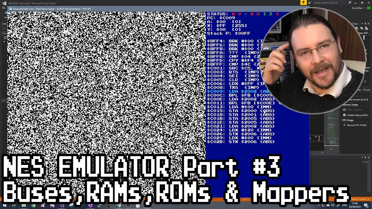











This video demonstrates how to implement a behavioral-level emulator for the 6502 CPU, focusing on the core components: the CPU itself with its registers (accumulator, X/Y registers, stack pointer, program counter, and status register), the bus system connecting the CPU to memory (RAM), and the instruction decoding mechanism using a 16x16 opcode table that maps each instruction byte to its corresponding addressing mode, operation function, and clock cycle count; the implementation covers all 12 addressing modes including immediate, absolute, zero page, indexed, and indirect addressing, with special attention to handling page boundary crossings and illegal opcodes, as well as implementing the complex addition and subtraction operations that require checking for overflow conditions using bitwise logic.
NES Emulator Part 2: 6502 CPU Implementation in C++
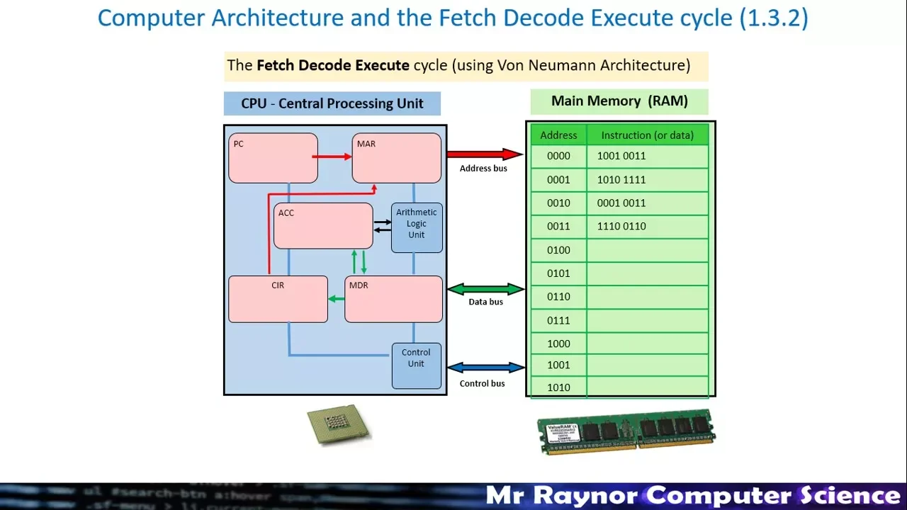
Added:hello I've decided to sit in the garden today because the weather's very nice it's too hot in the man cave to make videos like this this is the second part of my nez emulation series and I'm going to cover the central processing unit it's quite a long video because there's a lot of detail to go through but I'm justifying it because according to YouTube this is also my 100th video and I like the way that the Stars have aligned to make that happen anyway enjoy and I'll see you at the end the 6502 cpu was created by mas technologies around about 1975 it became the CPU of choice for many home computer systems and home console systems and in my case the Nintendo Entertainment System when you begin to emulate a CPU you need to decide what level of abstraction you're going to design at for example for my emulator I am uninterested in the electrical behavior of this CPU for my emulation I don't really care whether the signals are active high active low edge detected level detected open drain or even what the voltage levels are so I won't be going into that kind of detail what I'm interested in is the behavior of this device a CPU like this in isolation is the easiest thing in the world to emulate it does nothing it is currently blind to its environment and other devices are blind to it so for a CPU to be useful it needs to be able to communicate with the outside world so I am interested in the signals that allow me to do just that the CPU can output an address and it can both read and write data data reading and writing shows the same inputs so an additional signal is required to indicate whether it's reading or writing finally in order to do anything at all the CPU needs a clock Kwok's force a CPU to change state on each one of these clock edges the CPU can evaluate if any data is on its input and respond accordingly to change its output the CPU has no intrinsic understanding if the input data it sees is correct it just responds to it and this raises a rather interesting philosophical pickle point you can't emulate the CPU in isolation we also have to emulate something else in its environment the 6502 is capable of outputting a 16-bit wide address and this exchanges data eight bits at a time bytes electrically the read and write signal is important but in our software emulation we're not going to implement it as a signal and hopefully that'll become apparent why later since the CPU on its own doesn't mean anything we need to connect it to something and in this case we're going to connect it to a bus a bus is nothing more than a set of wires and connected to this bus are the address lines of the CPU also connected to the bus are the data lines when the CPU sets the address of the bus it expects all the devices connected to the bus to respond either by putting some data on the bus themselves so the CPU can read it or by accepting the data that the CPU itself has put on the bus this direction is of course governed by the read and write signal so that means we need additional devices on this bus here are three more devices I don't know what they are or what they do but what I do know is that this device can only write data to the bus this device in the middle can both read and write data to the bus and this device at the end can only read data from the bus the full addressable range of the bus is the full 16-bit address space that goes from 0 to F F F F devices that are connected to the bus need to have an awareness of their place so let's say this first device only responds to addresses in the range 0 to 7 F F F this next device is sensitive to a triple zero to say B F F F and this final third device is sensitive from C 0 0 0 to e F F F F when the CPU outputs the address 3000 on the bus this device is sensitive to it and will deposit some data on the bus and that data can then be read back by the CPU the other devices don't care about this address so they don't do anything if the CPU outputs the address 9000 on the bus and also writes some data in this case let's have a a then this device responds but because the CPU is writing this device knows it's being written to let's say the CPU finally wants to interact with 0 F F 0 0 there's no device connected to the bus that exists in that range if the CPU is writing some data so what nothing happens if the CPU is reading some data then it's effectively reading noise or more likely it's reading the previous state of the bus either way it's invalid data and if this scenario arises then the programmer has done something wrong because they are well aware of all of the hard work connected to the bus because the CPU can't work in isolation it's got to collaborate with other devices specifically for this video I'm going to assume there is only one connected device this device can both be read and written to and it covers the full addressable range and very simply it's going to be random access memory RAM and in a6 phone Evo 2 based system Ram is very important effectively we have 64 kilobytes of it and not only is it going to contain the variable information we might use in our programs it also contains the program's themselves which is a fairly traditional von Neumann architecture this implies that most of the time the CPU is indeed extracting bytes from the RAM in order to execute them as parts of its program and periodically it reads and writes to different locations to act as temporary storage already we can see that even for a simple emulation we need three components the CPU a bus and something that can provide the pro Grahame in this case is going to be Ram it could also be various connected devices which as we'll see later in the series for the nez there are a number of different devices connected to the bus I'm fortunate enough to have learned how to program originally on a 6502 processor in the form of a BBC model B micro but it was great to see the original datasheet of one of these devices for example here on the pinout diagram we can see these 16-bit addresses a 0 to a 15 and we can see 8 data bits d0 to d7 we can also see a pin labeled read and write there are few other pins too and we'll talk about those later the data sheet also contains what's inside the 6502 core itself there are three primary registers the accumulator the X register the Y register and these are all 8-bit even though they have different names they're all functionally quite similar they store in 8-bit number in addition we have a stack pointer a program counter and a status register the status register contains various bits that allow us to interrogate the state of the CPU things like what's the last result equal to zero has there been a carry operation and we can also instruct the CPU how to do things such as enable or disable interrupts and we'll look at interrupts later these are all individual bits and for convenience I'm going to package them into an 8-bit word the program counter is a 16-bit counter and it stores the address of the next program byte that the CPU needs to read naively as the program progresses the program counter increases in value things such as jumps and branches can directly set the program counter to jump and branch to different parts of the program like an if statement in C the stack pointer is an 8-bit number that points to an address somewhere in the memory and this address is incremented and decremented as we push and pull things from the stack the datasheet has a nice block diagram of how all of the various parts of the sesor work together but for our emulation were not interested in the majority of it don't forget this is really an electrical schematic and we're not emulating at the electrical circuit level it would be lovely to think that each time the CPU is clocked it outputs its program counter on the address plus receives a single byte of instruction does some internal magic to perform computation and if necessary output some data but no the 6502 does not operate this way it has two components which have a high degree of variability firstly not all the instructions are the same length some are one bytes some are two bytes and some of three bytes this means that the program counter is not simply incremented per instruction and since we need to do multiple things in order to get the instruction we're going to need several clock cycles and this is where the second variability is different instructions take different numbers of clock cycles in order to execute this means that per instruction we need to be concerned of the size of the instruction and its duration the 6502 has 56 legal instructions and I'll explain what that really means later on but these 56 instructions can be mutated to change their size and duration depending on the arguments of the instruction fortunately we can rely on the first byte of the instruction providing us with this information and we'll need this information in order to accurately emulate the instruction 6502 instructions look something like this let's take a classic instruction load the accumulator and I'm going to load it with the numeric value 65 and if you're wondering how I've got to that go and watch the previous video in this instruction I'm providing the data immediately so it can read one byte of the instruction and one byte of the immediate data therefore I can assume that this would be a 2-byte instruction I might want to load the accumulator from an address in memory though and memory is 16 bits so here I'm loading the accumulator using a value from this absolute address maybe we have one byte that represents the instruction but then we need two bytes to provide that instruction with the information that it needs in order to compute some instructions such as clear the carry bit in the status register don't require any data and so this can be represented using a single byte what we can see here is that for a given instruction there are a variety of ways to address the data that the instruction requires here I've shown two but there are in fact quite a number of them so even though functionally the instruction is the same it's represented differently so it can identify how to address the data therefore for a given instruction we need to emulate both its function and its addressing mode as well as the number of cycles it takes to implement fortunately we can identify all of this information from the first byte looking back at the data sheet here are the instructions and these are called the mnemonics these are the textual versions of the instruction this is how you would type them into your program before you compile it and later in this video I'll quickly go through all of these the 56 different functional instructions are mutated by the addressing mode and as I mentioned earlier there's quite a few different ones and we'll look at those two conveniently we can represent the instructions in a sixteen by sixteen matrix this of course gives us 256 potential instructions the first byte that we read can be used to index this table the lower four bits of that byte represents the column and the top four bits represent the row in my example I use the instruction load the accumulator 65 which was an immediate data source and I can zoom into that here the datasheet is quite old and it's been photocopied so that's why the quality isn't that high so the byte that represented that instruction has now told me where it resides in this table and this table entry tells me the instruction is load the accumulator and it's using the immediate mode it also tells me this - here how many clock cycles are required to implement that instruction and it also tells me how many bytes that instruction is elope this number is nice to know it's less relevant in the emulation here we've got set enable interrupts which was a very simple instruction it sets a flag in the status register it's of course implied the data source so it's only one byte in size but requires two cycles to execute next-door to it we've got a more complicated instruction this is add with Carrie and it's using something called the absolute addressing mode with Y offset which I'll detail later on this potentially takes four clock cycles and is a three bytes instruction the four has a little caveat to it and again when I talk about addressing modes later we'll see why but for now potentially this four can become a five it depends on where the data is being read from this fantastic table provides all the information we need to build the scaffolding for our emulation interestingly you'll notice that a blank spaces at the beginning of this video I said the CPU is oblivious to the data that it sees it'll just do whatever it can with what it sees it doesn't know if it's right or wrong if the eight bits that it reads at the start of instruction have an entry in this table that is considered a legal instruction a legal opcode however if there was eight bits resolved to one of these empty spaces that is an illegal opcode the CPU will still do something but it was not something the designers intended to happen there is a reason CPUs take multiple clock cycles to implement instructions in effect they run tiny little programs of their own internally and each stage of that tiny little program requires its own clock cycle so that's why we see more complicated instructions like this exclusive or within Direct X addressing requiring more clock cycles than simple instructions such as this one decrement the Y register those little programs need time and the clock in order to operate but why is that relevant to these illegal op codes well a CPU in reality is not like a big switch case statement in C or C++ it doesn't know that the bits it's seeing for its program bite are invalid it uses those bits to configure its internal arrangement and start its little internal program its micro code program and so these illegal op codes will do things but they'll do interesting and unexpected things and in some cases that people have found uses for the illegal op codes although I'm not going to emulate them for my implementation I found a slightly more modern data sheet for a slightly more modern chip but it's backwardly compatible with the 6502 and this provides the information I need in order to facilitate what the instructions should do needless to say data sheets are an amazing source of information they contain everything you need to do almost to emulate this device so the sequence of events is as follows we're going to read a byte at the program counters location I'm going to use this byte to index an array which represents the big table to get me the addressing mode and the number of cycles once I know the addressing mode I'm going to read any additional bytes that I need to complete the instruction then I'm going to execute the instruction I'm going to actually perform the computation on all of the data I have to hand and for my emulator I'm then going to wait and count clock cycles until the instruction is officially complete whereas the hardware 6502 will take time and break this up and do it all during the duration of the instruction I'm going to do it all at once let's start writing some code but just before I begin I want to emphasize the fact that I cannot possibly cover every single byte in a single video so I will be bringing code in at quite a fast pace in this video I'm hoping to demonstrate the core idea and the concepts and some of the peculiarities of the 6502 as usual there is code accompanying this video available from the one line code to github and there's a link in the description below unlike a lot of my videos I've gone to an extra special length to comment as much as I can the code that I am going to be demonstrating and I've written this it 5:02 emulation in a way that it should be educational and easy to follow every function is documented and where there are particular complexities I've gone to additional details even to the extent of explaining the logic operations of certain functions as a result I'm going to be bringing in code pretty quickly I'm starting the project with a blank int main and I'm going to straightaway add to the project two classes one is called bus and the other I'm calling olc 6502 before I even start looking at the CPU I'm going to flesh out the bus because it's quite simple one of the major difference between this series and my other videos is I'm going to be using the C standard integer library this renames the standard types such as int and short and unsigned char etc into explicit types we know the bus is written to and read from by the CPU so I'll add two functions right which takes a 16-bit unsigned integer as an address and an 8-bit unsigned integer for the data reading from the bus returns an 8-bit data takes a 16-bit address and for now and I'm just going to ask you to ignore it I'm also including a flag called read-only but for this video that's not going to do anything and so I've defaulted the parameter to false we can just pretend it's not there one of the reasons we don't need to emulate the read and write signal is this is implied by which function is called we're either writing to the bus or reading from the bus connected to this bus I have devices naturally the primary device is going to be the OLC 6502 cpu I'll include that up here and specifically for this video I've only got one other device and it's a 64 kilobyte Ram which I'm creating using a standard array if you try this for yourself you may run into a slight warning because this is asking for a large amount of memory to be placed on the stack however my compiler is fine with it so I'm going to run with it because I'm using a standard array I can iterate through it to reset its value this is just in case I'll set it all to 0 and I'll provide bodies for my write and read functions since the only device on my bus is my RAM I can simply sit straight away using the address and setting the data but I'm going to add something which is fundamentally useless for this video but very important later in the series I'm going to guard that RAM with a particular range in this case it's the full range so even though this line looks pointless I want you to get used to seeing it because we're going to be using lots of lines like this later on reading from the bus is very similar I just returned the contents of the RAM for a given address and even though we can't do it right now if we did read outside the range I'm just going to return zero now I need to connect the CPU to the bus I'm going to forward declare the bus an add a function called connect bus which stores a pointer to the bus privately to the class I'll now add to the CPU two more functions read and write they're the same as before the OLC 6502 class body will be responsible for calling internally these read and write functions and so for read I'm just going to call the buses read directly likewise for the write it just calls the buses right this layer of indirection may at first seem a little clumsy but it's very easy for you to create your own bus classes and use this 6502 emulation class in your own projects when we create an instance of the bus we can now connect the CPU to it and that's all we need for the bus whenever the CPU calls its read and write functions internally they'll be mapped onto the read and write functions of the bus and therefore interact with the RAM device that we have connected to the bus it's now time to start adding the core components of the CPU I'm going to start by creating an enumeration of the bits of the status register in bit zero we have the carry bit this is set either by the user to inform an operation that we want to use a carry bit or it is set by the operation itself we have a zero bit which is set mostly whenever the result of an operation equals zero when we set the I flag we're disabling interrupts the D flag is decimal mode and I'm going to point out now my 6502 emulation does not implement decimal mode so this flag is largely redundant the nez used a slight variation the 6502 processor and it didn't have decimal mode in hard work so I've chosen not to emulate it I might come back to this in the future and implement decimal mode so this is a true 6502 emulation the B flag indicates that the break operation has been called we have a flag here that is you that's unused finally we have the V and n Flags and these are used if the programmer decides to use the 6502 with signed variables and I'll talk about those later now define the flags I'm going to create an 8-bit variable called status to represent the status register whilst I'm here I'm also going to add in the other registers the accumulator the X register the Y register the stack pointer and the 16-bit program counter for convenience I'm also going to add a skate flag and set flag function which simply wraps up the bitwise operations to set the bits in the status register depending on the flag we're interested in for each instruction I'm going to emulate the addressing mode and then I'm going to emulate the operation and I'm going to wrap all of these things individually into functions in total there are twelve addressing modes and we've seen a few of these already some instructions have an implied data source some instructions have an immediate data source some instructions directly access the memory address using an absolute value and I hinted it some more complicated addressing modes and I'll talk about those as I implement them next to the addressing modes we have the opcodes and there are 56 of them have a function for each one of the mnemonics that we saw on the datasheet well what function should we call if we get an illegal opcode I'm going to catch all of those in this Triple X function we've hunted a lot of functions now but there's still a few more to add there are other external signals we want to do things on clock cycles so I need a function to indicate to the CPU that we want one clock cycle to occur there are three other inputs on the 6502 which we must implement the first is a reset signal the second is an interrupt request signal and the third is a non-maskable interrupt request signal all three of these functions can occur it n time they need to behave asynchronously and they interrupt the processor from doing what it's currently doing however it will finish the current instruction its executing depending upon the type of interrupts various things on the processor change and I'll talk about those as we implement these interrupts standard interrupts can be ignored depending on whether the interrupt enable flag is set or not non-maskable interrupt can never be disabled I've completed now the outward-facing functionality of the chip but we're going to need some internal helper functions to facilitate the emulation it's possible that the instructions use data and so we need to be able to fetch that data from the appropriate source and any data that I fetch I'm going to store in this fetched variable depending on the addressing mode we might want to read from different locations of the memory so I'm going to store that location in this variable on the 6502 branch instructions can only jump a certain distance from the location where the instruction was called so they jump to a relative address I'm going to add a variable to store the opcode I'm currently working with and another to store the number of cycles left for the duration of this instruction and for the last time I'll stress again if this is going too quickly please do consult the source code available from the link below it's highly commented and details exactly what all of these variables are for there's only one thing left to add now and that is the sixteen by sixteen table of opcodes I'm going to create a struct called instruction and it contains a string which holds the mnemonic I'm storing that in here because as part of my 6502 emulation and I'm not going to be showing it in this video I've also added a disassembler so it can reverse-engineer the compiled code into a human readable form I've added a function pointer to the address mode which we did here I've got a function pointer to the operation to be performed which is one of these and I've got a count of the number of clock cycles the instruction requires to execute I could create a big array of these but I'm just going to store all of these in a vector called lookup now let adding some implementation now a little warning I'm going to add some code which will cause you to spit your coffee all over your computer so please look the other way whilst I paste this in this is the populated sixteen by sixteen matrix and as I've stressed all along I've not tried to do this in a particularly clever way or an elegant way it is in a way which is easy to modify and easy to study the table is an initializer list of initializer lists and I'll show you that it corresponds to the table in the datasheet so here we've got break or blank blank blank or shift left and likewise we've got break or blank blank blank or shift left so each one of these entries contains all of the information we need the mnemonic the function pointer to the function that will implement the operation the function pointer to the address mode which will get the relevant data and the number of clock cycles the way I've implemented this all of my functions are class members so in order to get the address I need to prefix it with the class so I'm using the using keyword to create a little naming variable just to keep this table a little bit more concise and for the curious it took me about two days to enter this information and I entered it incorrectly and I needed my wife to double-check it all for me so thanks to her I'm now going to add the clock function because without this nothing will happen at all each instruction requires several clock cycles in order to execute but I'm only going to do the execution when my internal cycles variable is equal to 0 when I have the list on the slides I said I was going to do everything in one go and this is it firstly I'm going to call the read function of the current program counter location to get the opcode this returns one byte and it's this one byte which we'll use to index the table more or less always when you perform a read you're going to want to increase the program counter so it's prepared to read the next byte using the opcode to index the table I'm going to set my internal cycles variable to the required number of cycles for this instruction and since we have function pointers stored in the table I'm going to use the opcode to call the function required for that address mode and likewise I can do the same for the functionality so this line here is actually a function call looking back at the header file momentarily you'll see that all of my addressing mode functions and opcode functions return a value if you remember on the datasheet some of the entries had a little caveat that depending upon the instruction being executed they may need additional clock cycles my functions return a 1 or a 0 indicating whether there needs to be another clock cycle so I'm going to capture that in a variable if both the address mode function and the operation function indicate that they need an additional clock cycle then I'm going to add that additional clock cycle to my internal cycle count this effectively prolongs the duration of this instruction every time we call the clock function one cycle has elapsed so I'm going to decrement that count so here we can see that we really are only executing an instruction at one point in time whereas the real Hardware will be executing the instruction over several clock cycles in a way this means my emulation is not clock cycle accurate but that's ok because at the start I said I'm modeling this in a behavioral fashion because there are 12 addressing modes and 56 instructions I can't possibly detail them all in this video but I will pick out some select few and to be honest most of the instructions are so trivially simple there's really not much to show but I will try and talk about some of the more complicated ones the first addressing mode is implied that means there is actually no data as part of the instruction it doesn't need to do anything however implied also means that it could be operating upon the accumulator so I'm going to set my fetched variable to the contents of the accumulator immediate mode addressing means the data is supplied as part of the instruction it's going to be the next byte all of my dressed modes are going to set my address absolute variable so the instruction knows where to read the data from when it needs to and so in this case it's going to read from the next next up we have zero page addressing pages are a conceptual way of organizing memory we know that for a memory address we're going to require 16 bits and this can be split into two 8-bit bytes the high byte of this address can be referred to as the page and the low byte can be referred to as the offset into that page there is some significance to pages in hardware because it will read one byte before the other but it is convenient to think in terms of pages they make natural boundaries for which to store data and so we can think of the entire address space as being 256 pages of 256 bytes 0 page addressing means the byte of data we are interested in reading for this instruction can be found somewhere in page 0 ie the high byte is 0 6 502 programs tend to have their working memory located around page 0 because this is a way of directly accessing those bytes with instructions that require fewer bytes and don't forget instructions consist of multiple bytes and each byte takes time to read so in order to optimize the speed of your program we can just read in the low byte of the zeroth page the next address mode is 0 page addressing with X register offset here the address supplied with the instruction has the contents of the X register added to it this is useful for iterating through regions of memory like an array in C the array itself has a base address but the index applied to that array offsets that address we also have a 0 page offset with y register addressing it's exactly the same except it uses the Y register sometimes you just need to specify the full address in its natural form so the address supplied with the instruction and it'll have to be a 3 by 2 instruction for this consists of the low byte and the high byte of the address I all these together to form a 16-bit address word in a similar way to the 0 page with offsets we have an absolute address with X register offset we read in the base address and we offset it by the contents of the Eck's register however this is the first time we've encountered a caveat in our addressing mode function if after incrementing with the X register the whole address has changed to a different page we need to indicate to the system that we may need an additional clock cycle and I woke this out by looking to see if the high byte is changed after we've added X to it because if it has changed it's changed due to overflow the carry bit from the low byte has been carried into the high byte therefore we've changed page and again as before we have the same sort of thing for the Y register now we're going to get to the complicated ones indirect addressing this is effectively 6 502 s way of implementing pointers I can assure you that these will be too complex to describe verbally so if necessary pause the video a look at the source code to understand what's going on here but effectively the supplied address with the instruction is a pointer I'm going to interrogate that location to get the actual address which is where the data I want resides so here I assemble the 16-bit address that stores another address and here I read the 16-bit data at the original address and that 16-bit data is the new address I know right now awkwardly given that we're at such an early stage of programming this emulator at this point we need to consider something the original designers hadn't intended there's a bug in the hardware you'll notice here the 16-bit address using for the pointer if the low byte of that address is equal to F F or 255 then to get the high byte of the final address we need to add 1 to it and don't forget if we add 1 to the high byte of an address we're effectively changing the page for this particular instruction that doesn't actually happen instead it ignores the plus 1 the fantastic nez dev wiki lists all of these indirect addressing modes in a more mathematically friendly way but from this wiki you can also access an interesting document created 1994 which lists some of the bugs on the CPU and this bug here is what's interesting program has discovered this bug early on and worked around it including nez games programmers we're almost done with the addressing modes now here we've got indirect addressing of the zero page with X offset the supplied address reference is somewhere in the zero page and from that location we offset that one byte address by the contents of the X register to read the 16-bit actual address we need for the instruction and rather confusingly we've also got indirect addressing of the zeroth page with a Y register offset and unlike all of the others we'll have had a Y complement to the X this one behaves differently here again we read a single byte which is an offset into the zero page we just read the 16-bit actual address from that location and we offset that actual address by the contents of the Y register and as we've had with a previous instruction as we're offsetting the absolute actual address we may cross a page boundary which makes this addressing mode a candidate for requiring an additional clock cycle the final addressing mode is a slightly odd ball one if the others haven't been already and it's relative addressing mode this only applies to branching instructions and branching instructions can't jump to anywhere in the address range they can only jump to a location that's in the vicinity of the branch instruction in fact it can't jump to anywhere further away than 127 memory locations because this address is relative and not absolute like all of the others I'm storing it in its own variable the single byte that I read back is effectively unsigned but in order to jump backwards it needs to be assigned datatype and as we'll see a little later on signed numbers typically have the first bit or bit 7 of the byte set to 1 so I'm checking for that explicitly here and if it is I'm then setting the high byte of the relative address to all ones this way I can be sure the binary arithmetic works out when I'm adding the relative address to the program counter later on if the branch requires that even if all this talk about addressing modes has completely confused you don't worry fundamentally all we're interested in is the number that's in address absolute or address realm because that's address points to the location somewhere in the addressable space and in our case that's just the RAM where the data that the opcode is going to compute resides and you'll also be pleased to know fundamentally the addressing modes are the most complicated part of this emulation with the address mode sorted it's now time to emulate the instructions since we now know were in memory the data we want lives we need to fetch it so I'm going to fill in my fetch function and I want to fetch data for all instructions except the ones that use implied address mode simply because there's nothing to fetch and I'll start with a very simple instruction bitwise logic and and this sets the principle for all of the subsequent instructions the first thing I'm going to do is fetch the data the fetch function populates my fetched variable I also return this value for convenience just in case I want to use this as an argument in another function in this case the and operation performs a logic bitwise and between the accumulator and the data that's been fetched and so that's very simple to implement in C once I've performed the computation I want to update the status register as required so if the result of the logic and resulted in all the bits being zero I set the zero flag and on the 6502 processor I'm also going to set the negative flak if bit seven is equal to one now we've just kind of hinted at that with the relative addressing but I'll come back to it in the next instruction so now we fetch the data computed it updated the status register we need to return whether or not this instruction was a candidate for requiring additional clock cycles and it turns out the logic and is looking at the slightly higher resolution data sheet and finding the and instruction we can see there's a little or next to it and if we look at what that means it tells us that add 1 to n if page boundary is crossed where n was defined as the number of clock cycles required so I'm going to inform the system that this instruction can potentially require an additional clock cycle and just as a reminder if we go to the clock function we can see we can add additional clock cycles if both the addressing mode and operation require it the next instruction I'm going to demonstrate is a branching instruction because they all follow pretty much the same pattern in this case it's the branch if the carry bit of the status register is set instruction so I check to see is the carry bit equal to 1 if it is I set the absolute address to be the current program counter plus the offset that relative address we were talking about earlier branch instructions are unique in that these will directly modify the cycles variable when a branch is taken that automatically adds 1 to the required number of cycles for that instruction but in addition if the branch needs to cross a page boundary it incurs a second cycle of clock penalty so branch instructions can potentially require two additional clock cycles and again we can see this information in the datasheet here's the BCS instruction and it's got the suffix 2 let's have a look at what 2 says 2 says add one additional clock cycle if the branch occurs to the same page and add 2 if it occurs to a different page all the information we need is here in this instance I've used my absolute address variable as a temporary because now I want to take the branch ultimately I need to set the current program counter to the calculated new location all of the branch instructions operate this way branch if carry clear branch if equal branch if negative branch if not equal branch if positive branch if overflowed branch if not overflowed let's take a really simple instruction next clear the carry bit it does nothing particularly interesting it just sets the bit in the status register and as you probably guessed there's a whole bunch of these too I'm really not going to detail every single function but there are two which are problematic and rather ironically the two of the most useful functions on the 6502 and that is addition and subtraction now I would forgive you for thinking how on earth could these be complicated instructions and you're quite right fundamentally they're not the premise of the addition instruction is to add to the accumulator some data fetched from memory and the carry bit by including the carry bit we can chain together additions of 8-bit words into larger bit words because if one overflows it'll set the carry bit and we can use that carry bit as an input to the next addition for example if my accumulator contained 250 and I added to that 10 we know that because we're limited to 8 bit numbers that's going to wrap around and give us the answer for but because it's wrapped around its spat out a carry bit and if I was working with 16-bit numbers which I can't store on the 6502 I can algorithmically add them by looking at them in 8-bit parts so if I add the too low bytes together which are both 8 bits that's fine that gives me some answer but that has the potential to spit out a carry bit which I then need to add to the two high bytes when I add those together and I can keep doing this and work with arbitrary precision numbers but it's not this that makes addition complex the designers of the 6502 realize that sometimes programmers might like to work with signed numbers and not unsigned numbers so if I take an 8-bit binary word we can see in normal circumstances this is 128 plus 4 equals 132 completely acceptable when we're working in the range 0 to 255 nothing new here however what if we wanted to work in the range minus 128 to positive 127 in this instance our 132 has wrapped around gone all the way through 1 to 8 and become - a hundred and twenty for this process of wrapping around is called overflow by going beyond the workable range that we've specified we've made the numbers somewhat meaningless so if we're using unsigned data this binary word will equal one hundred and thirty-two but if we're using signed data its equals minus 124 and when we're working with signed data one way to realize if the number is indeed signed is to look at the first bit now you might be thinking that changing the workable range requires all sorts of specialist hardware but it doesn't the math still works out so we know that this is equal to 132 or it's equal to minus 124 let's add a number to this and see what happens regardless of the range we're using this number is equal to 17 if I add these together that becomes 1 0 1 0 1 0 0 1 which is equal to 149 here and in our signed representation is equal to minus 107 so the hardware doesn't change just how we think about representing the numbers has changed and we get the correct result in both circumstances and this is a very useful thing because it allows us to work with negative numbers even though our 8-bit processor only supports unsigned numbers to assist us further the 6502 provides two flags firstly and as I hinted at earlier if the result of an operation has the most significant bit set then that sets the negative flag so that tells the program and we'll hang on potentially if you are working with signed numbers then the result happened to be negative so that's useful but there's a more important principle here and this is the tricky part let's assume I'm now only working with the signed ranged numbers if I take a positive number and add it to another positive number if the result is positive all is good but because the largest positive number we can represent is 127 it's possible to add two positive numbers together and go beyond that Ray in which case it's wrapped around and the result goes negative this is meaningless and is called overflow numerically the result doesn't make sense if I take a positive number and add it to a negative number I can't possibly overflow and I'll leave you to work out why symmetrically if I have a negative number and I add it to a negative number and I end up with a negative result that's good but if I take a negative number and add it to a negative number and end up with a positive result again I've wrapped around and I've overflowed so the v-bit of the status register represents overflow which indicates if the result of the addition or subtraction operations when considered using signed numbers become nonsense we can compute this with bitwise operations so I'm going to build up a small truth table I'm going to take the value in my accumulator the value of the data that I'm adding I'm going to assume the carry bit is zero just to keep this sensible and also the result and what I'm going to look at is the most significant bit for each of these bytes I'm going to create an additional column which is whether the overflow bit should be set and it's filled out like this if the accumulator had a positive value and I added a positive value to it and the result was positive then nothing has overflowed if my accumulator had a positive value and I added a positive value to it but the most significant bit of the result was set that means it's negative then we have overflowed and we can continue down the truth table filling in the relevant bits and what we see is the overflow bit is only set for two situations so I want to derive a logic formula that gives me these results well to begin with I can see that the ones are set if the value in the accumulator is not the same polarity as the value in the result I can represent that as the exclusive-or between the accumulator value and the result which gives me 0 1 0 1 1 0 1 0 if I analyze the accumulator X Susa ford with the data were working with then I get this result if I invert this then what I can see is a situation where if this column and this column are true then I want to set my overflow bit therefore I can deduce that the overflow bit can be set when the most significant bit of the accumulator exclusive odd with the most significant bit of the result and not the most significant bit of the accumulator exclusive odd with the most significant bit of the data and this will tell me if I have overflowed so let's go back and populate our at instruction I'm going to fetch the data and then going to perform the addition and I want to perform addition in the 16-bit domain so I'm going to cast all of my little variables into 16 bits this allows me to easily check if I need to have a carry bit out because the high byte of the 16 bits will have a bit set in it so I can set my carry out flag the zero flag is set just as it was before and we now know that the negative flag equals the most significant bit of the low byte of the result the overflow flag well that's what we've just worked out the exclusive force between the data and the accumulator the data and the result and we're looking at the most significant bit of the low byte finally we can store the result back into the accumulator and as it happens the add instruction also has the capability to require an additional clock cycle so in case you've just whizzed through all of that the actual addition side of it is quite trivial but setting the overflow flag isn't now we have subtraction and don't worry this is complicated but it's almost identical to addition in principle subtraction is performing the following taking the accumulator subtracting the data and then also subtracting the opposite of the carry bit because in this case it's a borrow bit when designing processors it's useful to reuse hardware we're available now I don't know if they do this on the 6502 where I've designed processors I would certainly strive to try and reuse the hardware so I'd like to use the addition hardware to perform the subtract so let's have a think about that for a minute I can rewrite this equation as a equals a plus minus 1 multiplied by all of that and if I just rearrange that again I end up with this so here we can see it's starting to look a little bit like the addition but here we can see we're taking our positive data and we need to make it negative if I take the number 5 and represent that as binary I can get the negative equivalent by taking the two's complement which is where I flip all of these bits and add one in the equation above we can see we've already got the +1 so I don't need to worry about that all I need to do is invert the data and this means our subtract operation is almost identical to our add operation fetch the data and I'm going to invert the bits of the data I've represented it in 16-bit form for the carry reasons as before so I just want to invert the bottom eight bits which I can do with the exclusive or function after that inversion it is exactly the same as the addition in the provided source code I've provided quite an extensive explanation of these two functions specifically I've added lots of detail to the add instruction because it sets the template for all of the subsequent instructions which are listed in alphabetical order in the source file we've now covered the most simple instructions and the most complex instructions there's not much left to cover now so we'll just quickly look at these stack instructions so PHA pushes the accumulator to the stack the stack exists in the memory so we need to use the right instruction to access the bus to deposit the data in the right place the 6502 has hard-coded into it a base location for the stack pointer and the stack pointer variable is an offset to that location so there is a region in memory that is expected to be used for the stack by this processor when we add an item to the stack we write it to that location and we decrease the stack pointer and as with all stacks once you've pushed something to it you might want to something off it which is the PLA instruction in this case we increment the stack pointer read from the bus the value that we need and we set the zero and negative flags as we do for most of the instructions this concept of having hard-coded addresses into the fabric of the Silicon of the chip it's quite curious but it's also exploited in other functions too looking back there are three additional functions which are effectively interrupt when reset is called it configures the CPU into an own state so I want to set my registers and stack pointer and status to a known condition but I also need to set the program counter and it might be convenient to think that the program counter just gets set to address zero but that might not be useful you might not have program memory at zero in your addressable range and it's quite unlikely anyway because if you remember the stack itself is set to an offset and the zeroth page is used for user programmable things we saw that with the addressing mode so it typically is the case that the program data resides somewhere further along in the address memory so we need to get that address from somewhere and when reset is called on the 6502 it looks directly to location fffc to try and read that 16-bit address the data at this location can be set by the programmer when they're compiling their programs so the chip knows that in the event of a reset it should always look at this address to get the address to set its program counter to I'm also going to add the reset point set some of my internal variables to 0 just to keep things clean and tidy and quite importantly interrupts and resets take time so I'm going to hard-code our cycles value interrupt requests are quite similar however these can be ignored if the disable interrupt bit has not been set interrupts don't reset the program instead what we want to do is run a certain piece of code to service the interrupt and we don't want to completely destroy our program State in order to do that so when an interrupt occurs it starts to write some data to the stack the first thing it right well it's the current program counter this takes two rights because it's 16 bits along with the program counter we also want to write the status register to the stack a few of the bits get set at this point to indicate that an interrupt has occurred and as with the reset a hard-coded address is interrogated to get the value of the new program counter so this forces the program to jump to a known location set by the programmer to handle the fact that the interrupt has occurred and as before interrupts take time the non-maskable interrupt is exactly the same except nothing can stop this from occurring so again it writes the program counter to the stack it writes the status register to the stack and it looks at this specific address to get the value of the new program counter so we've seen now that specific addresses within the addressable range of the 6502 have dedicated purposes when the program has finished servicing an interrupt it'll need to return from it and this restores the state of the processor to how it was before the interrupt occurred which means we now need to read the status register from this stack and we need to read the previous program counter from the stack and set it and our program will continue as normal it got interrupted did something else and then went back that just about covers all of the different instruction types and functionality of the 6502 emulation i've not detailed every instruction most of them are quite trivial and similar to others so let's see now how we can test to see if this works I mentioned earlier that in the provided code I've included an additional function called disassemble and this will look at a specific range of addresses and turn the binary code into a human readable code this is invaluable for debugging as it allows you to step through the code and really see what's going on I'm not going to go into the details of what this function is actually doing but it's leveraging the address mode functions that we created earlier in order to decode the code in the right order fundamentally it retains a container of strings that represent the decompiled program now it's time to see if the emulation works to test the emulation of the CPU I've created a small pixel game engine project just to help visualize what's going on and I'd like to reassure you that this project does not do anything for the emulation it purely visualizes the state of the CPU now I know some of you won't know what the pixel game engine is but it's a utility that I've used on many videos in my channel it just displays pixels on the screen and allow simple acquisition of user input it's also very cross-platform so it'll compile for Linux and Windows and all you need to do to use it is include a single header file once it's included there are two functions you must overwrite on user create which is called once that the application starts up and on user update which is called every single frame to the class I've added some utility functions like this function that will convert a number to a hexadecimal string because the modern C++ way of doing this is absolutely appalling I've added a function that draws the contents of RAM another one that draws the status of the CPU so here we can see all of the status flag bits in it'll draw those green or red depending on whether they're set and we can also see the internal values of the registers of the CPU the most complicated function here is the draw code function which looks through the disassembly of our compiled program and displays that on the screen so really the real business happens in the on user creates and on user update functions one user update clears the whole display and then it's responsive to certain keys being pressed so if the user presses the spacebar it's going to provide enough clocks until that particular instruction is complete and then I've mapped the our iron n keys to the reset irq and non-maskable interrupt features of the CPU finally all I'm doing is drawing the RAM for the zero page drawing the RAM for the page residing at eight triple zero draw the CPU state to draw the code and draw the instructions on the screen in on user create I prefer the RAM for execution this is the program I intend to run it's not optimized it just allows me to test a couple of features at once and it held back to my what is assembly language video because I'm going to multiply 10 by 3 on a system that doesn't have a multiplier there's loads of 6502 assemblers available but I like this one because of its simplicity you can take your 6502 program and paste it into the source code window click the generate code button and it shows you how it's assembled the code very conveniently it will also produce the object code in a string format so I can copy that code and paste it into a string this line at the start of the program tells the assembler were to put these instructions in memory so I'm looking at page 80 as I read in the string hex word by hex word undeposited them into the ramp at the right location it's important to remember we also need to set the reset vector so when the reset occurs it knows to look to page 84 the first line of code I then run my disassembly routine and I call the reset function on the CPU so let's take a look this is the display in the top left we have a memory window which shows the zero page and down here on the bottom left we have page eighty and we can see the program memory has been loaded to that location in the top right we can see the individual bits of the status register the program counter the internal registers and the stack pointer and here on the right hand side we can see the disassembled program and this should resemble the program that we input it into the assembler the objective of this program was to multiply 10 by 3 and it's not optimized because I wanted to test the variety of features so the first instruction that's going to be run is the LDX instruction and that's going to load a into the X register which is 10 compress the spacebar to step to the next instruction but up here we can see that the X register now contains the value 10 st x stores the contents of the X register to an absolute memory address in this case it's going to be at the 0 location in page 0 but execute that instruction we can see that a has been written to that location now I want to load into the X register at the value 3 and store that at location 1 I'm going to load the value from location 0 into register Y so we can see here why is now loaded location zero and has become ten and I'm going to set the accumulator to zero just in case it wasn't already and you can see that by setting the accumulator to zero the zero flag got set just in case the carry bit has been set I'm going to clear it and now I'm going to call the very complicated addition function to take data from location one in the zero page and add that to the accumulator so it's going to read in this three and add it to the accumulator up here there we go I'm now going to decrease the value of the why register by one the branch not equal instruction effectively checks to see if the zero bit has been set if it hasn't then the branch is going to be followed and in this case it's branching with a relative address because that's what branches do to a location a few lines earlier we know it's going to jump backwards because we can see here that it's F a is the relative address and so because it begins with a 1 that binary string it must be a negative number and we do indeed see it as jumped back to a t10 word now again it adds to the accumulator so the accumulators had 3 added to it again it's become 6 we decrement the Y and we keep doing this until Y has become 0 so now when Y has been decremented and it's equal to zero the zero flag has been set the branch isn't followed I'm going to store the result of the accumulator in address 2 which is 1 e which in decimal is 30 so we've multiplied 10 by 3 and got the result 30 I can press the our key to reset the CPU it doesn't reset the contents of the memories and because on computing systems like the nares and others you don't know really what the values in the memory are going to be so never take that for granted and that's why you should always write to the memory the values that you expect to be there with this little utility it's very easy to sanity check the individual instructions and it does take some time but in doing so you'll become quite familiar with the 6502 assembly language once your emulator has matured to a certain level it becomes possible to start using available testing roms these are programs deliberately compiled to try and find errors in your emulation components and they're created by rather famous people in the nez emulation scene such as blog and bisquit one of the easiest to use tests for the CPU is nez test by Kevin Horton if your emulation has graphical capability it will show you on the screen which instructions have failed if you don't have graphical capabilities yet it sets specific memory values that you can interrogate and it set certain values with specific numbers to tell you which instructions have failed and how they have failed in my completed emulator I'm going to load the nez test as wrong in its own right this ROM is a great way to start testing the graphical capabilities of your system because if you can see it then you know you're on the right track and we'll talk about that in the next part of the series but for now I want to run all tests and we can see the emulation that have created of the 6502 for the nez passes them all let's say I deliberately sabotage one of my instructions now if I run the same test suite and run all tests we can see they haven't passed one of them has failed with the code 42 this code is also available somewhere to read in the nares memory if I consult the documentation for the nez test ROM and look for error 42 it says the instruction ta X did something bad um in this case it messed up the flags and that is indeed exactly how I sabotage this instruction I best put that back before I forget and so there you have it a cycle accurate emulation of the parts of the 6502 processor that the nez needs if you're still watching thank you very much and as you can see it's not that trivial one of the things I'd like to point out is that the magic of video editing can make this look like a very smooth and quick process but rest assured it isn't it was a complicated and long process in fact this was actually the third attempt at creating the 6502 but I undertook this is my 100th video and I'd like to thank all of those that have supported the channel so far I really didn't think I would end up making hundred videos but I've no plans on stopping anytime soon as always all of the source code for this video is available from the link below on the water loan code at github have a think about subscribing and if you've liked this video please give me a big thumbs up come and have a chat on the discord server and I'll see you next time for part two where we're going to start looking at drawing things to the screen
Up Next
Modern C++ Techniques for Legacy Code: An Emulator Case Study | ACCU 2025 Keynote
@ACCUConf
25.1K views•2025-08-29

Introduction to Secure Multiparty Computation with Yehuda Lindell
@fhe_org
7.7K views•2021-02-04
Convex Polygon Collisions: AABB and Separating Axis Theorem Explained
@javidx9
136.4K views•2019-02-02
Enigma Machine Mechanics: WWII Encryption Explained
@JaredOwen
13.2M views•2021-12-11
Related Study Plans & Knowledge Roadmaps
Structured learning paths in Computer Science