














![[Основы ОС, практика] Устройство памяти 2](https://i.ytimg.com/vi/LUrXQgBTSbs/maxresdefault.jpg)









Computer memory operates on fundamentally different physical principles depending on its type: SRAM uses six-transistor SR latches for fast, static storage without refresh; DRAM uses one-transistor-one-capacitor cells requiring constant refresh cycles due to capacitor leakage; HDDs store data magnetically on spinning disks using ferromagnetic materials; and flash memory uses floating-gate transistors with quantum tunneling to achieve non-volatile storage, with multi-level cell technology enabling multiple bits per cell through varying electron charge levels.
Physics of Computer Memory: SRAM, DRAM, SSD, HDD Explained
Added:Basic semiconductor physics, including the operation of transistors (specifically MOSFETs) and capacitors.
Fundamentals of electromagnetism, particularly magnetic polarization and how magnetic materials store physical states.
The concept of binary data representation, understanding how 0s and 1s are mapped to physical properties like electrical charge or magnetic orientation.
The fundamental distinction between volatile memory (requires power to maintain data) and non-volatile storage.
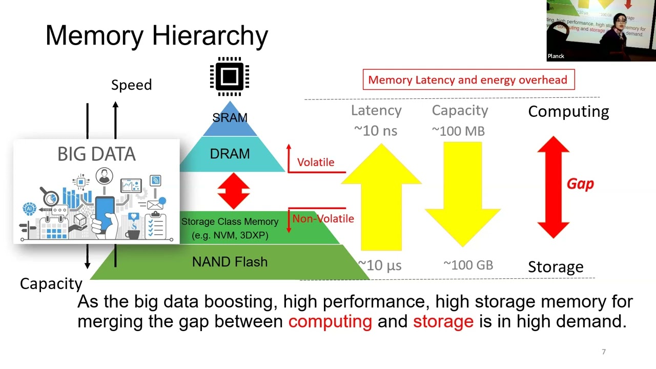
Memory hierarchy design in computer architecture, exploring how CPU caches (L1/L2/L3), system RAM, and persistent storage interact.
Advanced flash storage management, including wear leveling algorithms, garbage collection, and Error-Correcting Code (ECC) systems.
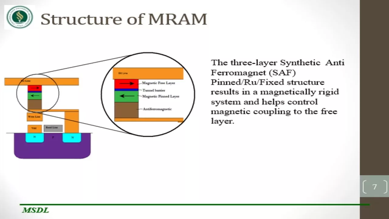
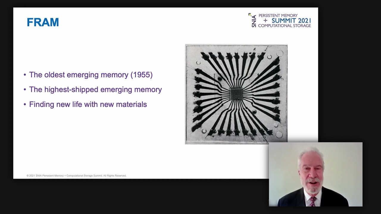
Emerging non-volatile memory technologies that attempt to merge RAM speed with persistent storage, such as Magnetoresistive RAM (MRAM) and Phase-Change Memory (PCM).
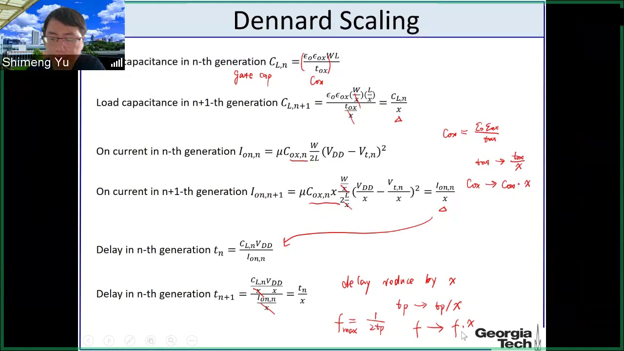
The physical scaling limits of modern silicon fabrication, such as quantum tunneling in sub-10nm NAND flash and leakage currents in DRAM.
1.5K views92likes36:49Original Release: 2024-03-10
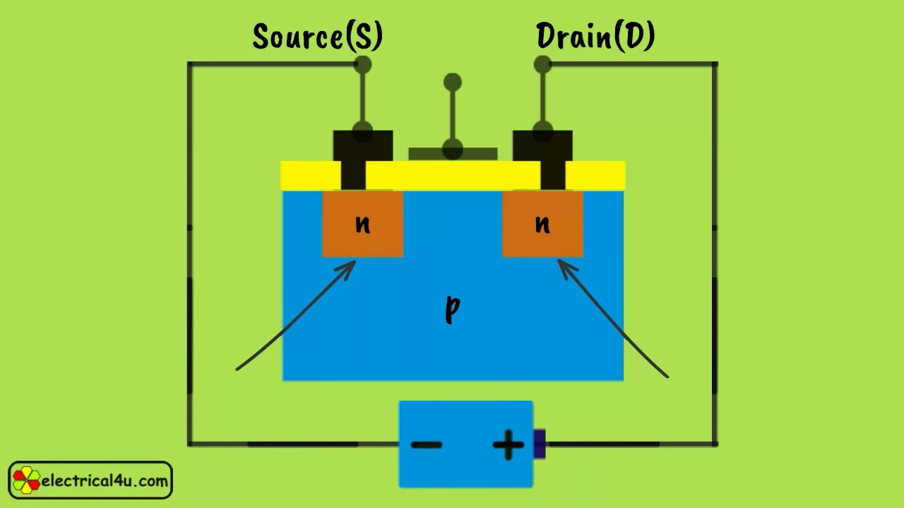
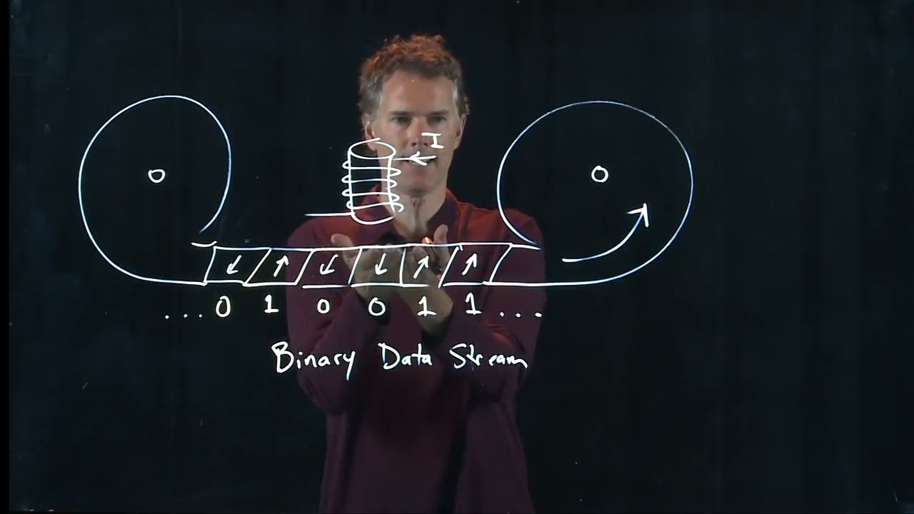
hello everyone and Welcome to our channel in one of our previous videos we discussed the physical principles underlying the device that is the Cornerstone of modern Electronics the semiconductor Field Effect transistor we also talked about how with the help of these devices or rather combinations of these devices known as logic gates we taught computers to perform basic operations such as addition and subtraction today we'll take a look at the physics of computers from a slightly different perspective and talk about how from a physical point of view a computer remembers or in other words how memory devices are structured in all their diversity as well as why a computer needs a whole bunch of different types of memory based on various physical principles subscribe to the channel and let's get started any memory device consists of cells Each of which typically stores only one bit of data that is one binary digit which can have a value of either zero or one and if we wrote One into our cell then at the output we should always have one regardless of the signal applied to the input until we send a signal to the cell to rewrite the stored data changing one to zero and now our cell will always output zero until we decide to rewrite it again it turns out that memory cells can also be created from the same transistors or rather assembled from transistors of logical cells to begin with let's consider the simplest transistor cell capable of storing information for this we will use the or logical gate which as we remember consists of just two transistors connected in parallel to each other in short I'll remind you that the O gate operates in such a way that it passes current to the output if there is voltage on at least one of its inputs or on both inputs at once and zero that is the absence of a signal will only be at the output if there is no voltage on any of the inputs so we have an O gate and all we need to do to turn the O gate into the simplest memory cell is to pass the signal from its output to one of its inputs let's assume that at the initial moment in time no signal is applied to the remaining free input accordingly no signals are applied to both actual inputs and we will also have zero at the output now let's apply one to the input since this is an O gate it's enough for us to have one on just one input and we will get one at the output and this one from the output will now be passed to the second input that is both inputs of the or gate will have one and the output will also be one even if we now disconnect the signal originally applied to the free input that is our modified o gate has learned to remember whether we have previously applied a signal to its input essentially we have created the simplest memory cell which I congratulate you and myself on but we have one small problem if we want to rewrite the value written by us in the cell then we cannot do this in simpler terms our cell does not support rewriting of information it is somewhat similar to a torn out sheet from a notebook on which something can be written but what is written cannot be changed we can only throw it away and take a new one dealing with computer memory in this way is of course impractical and we need to improve the scheme somehow there are several ways to do this and here we will consider only one of them for this we already need two or Gates each consisting I remind you of two transistors as well as two notot gates with one transistor each connected to each of the or Gates I remind you that the combination of an or gate and a not gate is called an or not gate and its result will be exactly the opposite of the result of the or gate operation it will output one if both of its inputs are zero and zero in all other cases let's connect our or not elements in such a way obtaining what is called an Sr latch from the English set reset these are the names of the inputs of the resulting logic circuit let's say at the initial moment in time we apply one to the set input and zero to the reset input which means that we are writing one into our scheme the first or not gate I remind you outputs one only if both inputs are zero in our case one of the inputs is definitely one that is the gate outputs zero this zero is passed to one of the inputs of the second or not gate and on the second of these inputs also zero because we did not apply a signal to the reset input two zeros at both inputs of the or not gate mean one at the output of this element and at the output of the entire scheme as a whole which is what we need in addition this one will be sent to the second input of the first or not gate this will not change change the result since if both inputs of the or not gate are one the result will still be zero but even if we now disconnect the set input the result will not change the first or not gate will still output zero at the output forcing the second or not gate to Output one you may ask where does the signal come from in the system when we don't apply anything after all a signal is essentially an electric current and for something to flow out of the system something must flow into to it and this is a completely correct and logical question and the answer to it sounds like this the current in the system is taken from an external power source which Powers our logic elements without external power all this will not work they say that the scheme is energy dependent and we will return to this issue later all right now let's try to rewrite our cell that is change the value stored in it from 1 to zero to do this we need to send a signal to the reset input and see what happens in this case the signal applied will reach one of the inputs of the second or not element and since now one of its incoming signals will be equal to one the outgoing signal will become zero this signal will be sent to the output of our cell as well as to the second input of the first or not scheme now on both of its inputs there will be zero meaning the signal outgoing from it will be one this one will go to the input of the second or not element effectively blocking it even if we now disconnect the signal we applied to the reset input the result will not change the scheme will output zero until we apply a signal to the set input indicating that we want to change the state of our memory cell back to one or until we disconnect the power which will erase the data stored in the cell Sr latches are not the only transistor-based memory scheme used in practice however as I mentioned our video is more about physics than about circuitry so we'll probably limit ourselves to that memory based on semiconductor transistors has high operating speed both writing to and reading from such memory occurs at the speed of transistor switching essentially with the same speed as the processor in our computer capable of Performing several billion operations per second meaning it has a frequency in gigahertz however this memory also has its drawbacks the key one is that that as we saw above to create a memory cell containing just one single bit of data we need a total of six transistors to write eight bits or one bite of data we would need 48 transistors and so on for example the Windows 10 operating system constantly uses at least gigabytes of data meaning 8 billion bits of data for which we would need 48 billion transistors which is comparable to the number of transistors in the computer's processor itself and therefore the cost of such memory storage would be correspondingly high in reality a modern computer needs much more memory so it is obvious that even from an economic point of view using only this type of memory is Not Practical furthermore as we mentioned earlier semiconductor memory requires constant external power and it also has a relatively low data storage density meaning that to store a large amount of data we would need a device of relatively large size therefore for in modern computers semiconductor memory also called SRAM from static Random Access Memory stores only a tiny fraction of the total amount of stored data it is used for the computer's own memory such as registers as well as for the processor cache registers store a very small amount of data that the processor is working with right now it's like a spoonful of soup that we scoop up and prepare to eat the cache stores data that the processor is currently working with or plans to work with in the near future the cash can be compared to a plate of soup that we are going to eat for lunch however the majority of the soup is usually still stored in the pot similarly the portion of data that the computer is currently working with is stored in registers the data that it plans to work with in the near future is stored in the cache and the main part of the data that the computer needs for operation is stored in the so-called main memory and this information pot of main memory is organized on slightly different principles instead of six transistors per cell here only one transistor is used as well as one capacitor capable of storing a certain amount of electric charge more precisely when the capacitor is connected to a circuit with voltage it accumulates charge and then when the voltage is turned off it can itself become a power source releasing the accumulated charge back into the circuit we won't de Del into the device and principles of operation of capacitors in this video in the most superficial approximation this is a well-known thing and if you look more closely there are many non-obvious things there which probably deserve a separate video in general if you would like to see a separate video about capacitors write about it in the comments and I will definitely make one here and now the main thing for us is this if the capacitor is connected in a circuit with a voltage higher than the vol voltage it is charged to it will draw some of the electrical energy and charge itself if the voltage in the circuit is lower the capacitor will release energy back to the Circuit discharging in the process and it is precisely this property of capacitors that is utilized to create memory cells based on them as a reminder it consists of a capacitor and a transistor as well as contacts connecting the cell to the Circuit more precisely there are two of these contacts S one is attached to the transistor's gate and depending on the presence or absence of voltage on it it is determined whether the transistor controlling the cell is in an open or closed position the second contact is connected to the line leading to the capacitor and through it reading and writing of data from the cell is carried out the state of the cell when it contains a one is considered when the capacitor is charged let's say to a voltage of 1.2 volts and if the Capac capacitor is discharged it means that a zero is stored in the cell to read data from the cell we open the transistor and pass a voltage through the read and right line that is slightly lower than the voltage of the charged capacitor let's say Let It Be 0.6 volts the charge capacitor has a higher voltage and will release the accumulated charge into the line causing the voltage in it to increase let's say to 0.8 volts on the other hand the charged capacitor will start to charge drawing energy from the line causing its voltage to drop let's say to 0.4 volts so if after passing through the capacitor we get a voltage higher than 0.6 volts then we know that a one is stored in the cell and if it's lower then it's a zero now let's see how the write operation will look like if we want to write a one to the cell we apply a voltage of 1.2 Vols to the corresponding line this will charge the discharged capacitor and the charged one will remain charged to write a zero we open the transistor with zero voltage in the circuit as a result the charged capacitor will discharge while the discharged one will remain discharged meaning we will get a zero in our cell as required however capacitors have one problem they tend to lose charge over time due to various reasons moreover in our device this process is exacerbated because during during each read cycle we drain a bit of charge from each charged capacitor and inject a bit of charge into each discharged capacitor therefore for capacitor-based memory a refresh procedure is also necessary during which slightly discharged capacitors need to be recharged to the maximum and slightly charged ones contrary to Our intention need to be completely discharged this data refresh procedure is in some sense a combination of read and write procedures first we determine whether a zero or a one is stored in a particular cell by applying intermediate voltage to the line and then we top up the capacitors in cells with ones by applying full 1.2 volts to the line and empty the cells where a zero is stored by applying zero voltage to the line after this we can be sure that all capacitors that should be charged are fully charged and all that should be discharged are discharged to zero this refresh procedure occurs constantly several thousand times per second to ensure that we don't lose any data the need to constantly update the information stored in capacitor-based memory determined its name dram or dynamic Random Access Memory the transistor cache memory on the other hand is called SRAM which stands for static random access memory as it does not require a refresh procedure of course what we have just discussed is only a very general description of the principles underlying Dr technology for for example in this video we will not discuss what sdram is which stands for synchronous Damm implying synchronization of the memory and processor clocks to explain why this is done we would need a fairly lengthy Excursion which lies more in the field of circuitry than in the field of physics and this is not quite what we do on this channel let's just say that today almost all dram is synchronized so when we talk about dram today we usually mean sdram also we we will not delve into the differences between DDR standards such as DDR3 ddr4 and ddr5 and so on perhaps it's worth mentioning that each subsequent generation of dedam uses increasingly lower voltage which positively affects the memory's power consumption instead let's talk about why both types of memory dram and SRAM are necessary in our computer drram has two main advantages over SRAM price and data storage density for example a dram module will cost about2 200 times less than an SRAM module of the same capacity and will have about 20 times smaller Dimensions these figures are quite conditional as these devices rarely have even approximately comparable memory capacities if we're talking about tens of megabytes of memory for Ram then in the case of dam it's already about tens of gigabytes which is a thousand times more so why not abandon expensive SRAM and switch to cheap Damm first of all because it operates about about 5 to 10 times slower and if a ram is capable of providing data to the processor almost as quickly as it needs it then when getting data directly from Dr the processor would spend most of its time idle waiting for the slow memory to find the necessary data that's why a compromise is made using a small amount of fast but expensive SRAM for the computer's operation and a significantly larger amount of relatively cheap but slower Dam the data needed for the processor Here and Now is unloaded from drram T Ram just like you pour soup from the pot into the plate to eat another drawback of dram is its high power consumption because it needs to be constantly Rewritten and this becomes an even greater problem as larger amounts of ram are used in modern computers and other electronic devices SRAM consumes less power but also requires constant power supply and if you turn off your computer the data will be lost and obviously this is unacceptable able you can't keep your computer or even some of its parts constantly turned on so you definitely need some means to save data when it is turned off that is in addition to static and dynamic memory we also need nonvolatile memory typically but not exclusively this memory is used for long-term storage of data that we work with from time to time and that may be needed by our computer in the future if SRAM is like a plate of soup and Damm is like a pot of soup now we're talking more about a refrigerator or for example a Cellar where we store potatoes cabbage carrots and other ingredients from which we can make soup when we need it and generally speaking we have enough supplies of these products for dozens or even hundreds of pots of soup but we don't cook it all at once but use it as needed today there are three main Technologies for long-term data storage magnetic storage solid state storage and Optical discs the ladder are practically OB obsolete today so we won't spend time on them as for magnetic storage the most common type used in personal computers today is the so-called hard disk drive or HDD by the way terminologically it's not very fortunate it's easy to think that a solidstate drive and a hard disk are the same thing just different words but no they are fundamentally different Technologies on a hard disk drive information is stored on small circular discs usually made of a magnesium aluminum alloy assembled into small Stacks the surface of each disc is covered with microscopic concentric tracks made of a ferromagnetic material usually a Cobalt chromium and tantalum alloy the tracks are divided into sectors and each sector is divided into cells Each of which contains one bit of data I.E zero or one data is written by magnetizing cells in one way or another making each cell a tiny magnet if we look at the disc as if it were cut the magnetization of the cell can be be directed upwards or downwards that is either inside the disc or outside between the unlike poles of the micromagnets in the magnetic cells a magnetic flux arises which we can register determining how exactly the cell is magnetized for example we can agree that upward magnetization corresponds to zero and downward magnetization corresponds to one or vice versa however this is not done today the point is that between adjacent cells with opposite magnetization a magnetic flux also arises which we can register but there is no such flux between identically magnetized cells and it turned out that it is easier to register the presence or absence of a magnetic flux between neighboring cells than to determine the direction of the flux between the poles of the same cell this means that we can register smaller magnetic fluxes that is use magnetic cells of smaller size and as a result achieve higher data density on the hard disk that is whether a zero or a one is written on this part of the disc depends on whether the read head registers the magnetic flux between this and the next cell that is the data carrier is not the cells themselves but the boundaries between them which are also called domain walls if there is a wall then the magnetization of the cells differs then we record one if neighboring cells are magnetized the same way then there is no domain wall and we say that zero is written additional reduction in the size of cells and increase in data density can be achieved by using super sensitive readed heads based on the giant Magneto resistance effect and relatively recently the capacity of hard drives has been further increased by improving the recording method through the introduction of the so-called heat assisted magnetic recording or Hammer if the first hard drives from IBM weighing about a ton could store only 5 megabytes of data then their modern descendants can now accommodate tens of terabytes or tens of trillions of bytes of data with more than modest sizes and most importantly cost the history of which Technologies exactly allowed hard drives to go such an impressive path May deserve a separate story and if you want to hear it again don't forget to write about it in the comments hard disk drives have impressive data storage density at a relatively low cost and also serve as nonvolatile memory meaning that the data written on them is preserved even after power is turned off however they also have their drawbacks the key one is speed while even relatively slow drram provides data transfer speeds of around 5,000 megabits per second hard disk drives offer about 100 megabits per second which is roughly 50 times slower than Damm not to mention the faster SRAM therefore it's essentially impractical for the processor to directly read data from the hard disk as it would be unimaginably slow by processor speed standards instead the computer first loads the required data from the hard disk into the RAM and works with it and after completing the task the modified data is Rewritten back to the hard disk on the other hand non-volatile memory is needed not only for storing user data the processor also has a certain amount of data required for its operation which would be useful to preserve even in the absence of power meaning there was need to create nonvolatile main memory an analog of SRAM or at least Damm in terms of speed but capable of retaining data even when power is disconnected initially so-called ROM readon memory was used for these purposes meaning memory accessible only for reading as the name suggests data written to such memory can only be read but not Rewritten in ROM microchips data was written at the factory and could not be changed thereafter this was not very conven venient for many reasons so the concept of pure ROM was abandoned first the so-called prom programmable readon memory was created which could be programmed but only once like being able to write data only once to our simplest memory cell made of one or gate as we started the story then eom erasable programmable readon memory was created which could even be erased and Rewritten but through various clever methods such as exposing the microchip to ultraviolet light finally the eom electrically erasable programmable readon memory technology emerged and the Pinnacle of nonvital internal memory Evolution became flash memory technology currently it has practically displaced all others and thanks to certain technological advancements it has even penetrated into other areas initially not intended for it and today the successors of the first flash memory chips successfully compete with hard disk drives how does Flash memory work work it also relies on Field Effect transistors but not ordinary ones but slightly modified ones so-called floating gate transistors so what is a regular Field Effect transistor essentially it's a piece of ptype semiconductor with two pieces of n type semiconductor embedded in it contacts are connected to both n type semiconductors leading to our circuit in addition another contact called the gate is brought on top of the region between the N type semiconductors which is necessary to control the transistor a layer of dialectric or insulator is placed between the gate and the Semiconductor in the ptype semiconductor the main charge carriers are positively charged holes although there are also some electrons present in nype semiconductors on the other hand these functions are performed by electrons although holes are present in them since the charge carriers and semiconductors of different types are different our semi semiconductor assembly will not conduct current just like that but if we apply a voltage to the gate creating an electric field directed downwards that is attracting electrons and repelling holes then something interesting will happen in the region of the ptype semiconductor between the two n type semiconductors all or at least most of the holes will be pushed out from there while a few electrons from the entire semiconductor will on the contrary be attracted to this area and although holes dominate in the ptype semiconductor as a whole in the narrow area under the gate and between the N type semiconductors an area will be created where electrons will dominate that is the narrow layer of ptype semiconductor will turn into an end type semiconductor and electric current will be able to flow through it it is said that the transistor will be opened now let's take a look at what a floating gate transistor is essentially it's the same thing but with an additional conductor inserted between the actual gate and the semiconductors in the normal state it doesn't affect anything by applying voltage to the gate we can still open the transistor and by turning it off we can close it but what if we somehow introduce a certain number of electrons into this intermediate conductor indeed when we apply voltage to the gate now the field will still attract electrons from the ptype semiconductor and repel holes attempting to create an n type conducting Channel however now this process will be hindered by the electrons in the floating gate which will repel electrons and attract holes in other words do exactly the opposite of what the voltage applied to the gate is trying to do the transistor won't open or more precisely to open it we need to apply a higher voltage to the gate so our device will operate differently depending on whether there are electrons in the intermediate conductor if they are present the transistor will remain closed even at the voltage that would open it if they weren't there thus by placing and removing electrons from the gap between the gate and the semiconductor we can change the state of the system if there are no electrons the current will flow at the working voltage on the main gate and we say that a one is written in the cell if electrons are present then at the same voltage the transistor remains closed no current flows and we say that a zero is written in the cell so essentially we've described how the read operation from a memory cell consisting of a floating gate transistor will look like we apply the working voltage let's say 3 volts to the gate and contacts and check if current flows if it does it means there are no electrons in the floating gate and a one is written in the cell if the current doesn't flow it means that the electrons in the floating gate hindered the creation of a conductor Channel and a zero is written in the cell now we just need to understand how we can place electrons in the isolated floating gate and remove them from it that is how the procedure of writing information to the cell occurs let's assume that a one is written in it that is the floating gate is empty and we need to fill it with electrons writing a zero to the cell to do this we apply a high voltage to our transistor let's say 10 volts in this case current will flow through the transistor as usual but the high voltage on the gate will attract electrons from the channel so strongly that some of them will jump from the channel to the floating gate how is this possible you may ask since the floating gate and the conducting channel are separated by a layer of insulator that electrons cannot pass through and this is the right question and the answer to it lies in the phenomenon known as the tunnel effect a quantum mechanical phenomenon that allows particles to sometimes pass through barriers standing in their way more about the tunnel effect by the way we had a separate video the link to which will now appear in the upper right corner of the screen and in this case thanks to the fact that we applied a large electric field some electrons from the channel will be able to Tunnel into the floating gate filling it and since the tunnel effect is purely quantum mechanical phenomenon not having an explanation from the standpoint of classical physics it can be said that familiar flash drives and other similar media are a vivid confirmation that quantum mechanics Works no matter how strange its laws may seem to us at first glance all right we've filled the floating gate with electrons rewriting the stored one to zero how do we now perform the reverse operation and remove electrons from the gate turning zero into one well essentially the same way only now we need to apply voltage in the opposite direction so that it pushes electrons out of the floating gate of course thanks to the same tunnel effect and what's remarkable is that our floating gate is isolated from other parts of the cell and to influence the number of electrons in it we need to apply significant voltages by the standards of micro electronics and if such voltages are not applied then there is simply nowhere for the electrons from the floating gate to go which means that the cell will retain the information written in it even when power is turned off that is the memory created based on such cells will be nonvolatile more precisely over time electrons will leave the floating gate thanks to the same tunnel effect however without an external voltage they will do so very slowly the floating gate can retain charge and the cell the data written in it for years furthermore to store one memory bit we only need one transistor as opposed to six in the case of sham making flash memory cheaper and providing it with a higher data storage density however a downside of this technology is that writing and rewriting data require significant energy consumption meaning while reading data from flash memory can be done easily and fairly quickly reading speed is in Nan similar to Sham writing poses a problem taking microc seconds which is roughly 1,000 times longer additionally each right cycle damages the insulator layer separating the floating gate and the semiconductor so flash memory has a limitation on the number of rewrite Cycles however since flash memory was originally intended for storing data relevant to the processor that was not expected to be frequently Rewritten this wasn't a major issue there are various ways of connecting flash cells into arrays of data called nor and nanan structures but this is more about circuitry than physics so we won't delve into that instead let's talk about how further development of flash technology has significantly expanded its application area allowing the creation of devices for long-term data storage the well-known USB flash drives memory cards and SSD diss that is those solid state drives we mentioned this was made possible by the discovery of a way to write more than just one bit of data to a single memory cell unlike in other cases but rather Two Three or even four bits as we've already discussed a flash cell with a zero written to it differs from a cell with a one in the amount of electrons stored in the floating gate if there are few electrons the cell stores a one and if there are many it stores a zero but why should we limit ourselves to just the categories of few and many why not try to measure how many electrons we've pumped into the floating gate and it turns out we can easily do that by applying different voltages to the main gate of the the transistor indeed let's say there are practically no electrons in the floating gate which means the transistor opens with the minimum voltage we'll denote this state as 1 one in binary notation or three in decimal if at this voltage the transistor remains closed but opens with a slightly higher voltage it means there are electrons but not many then we'll say that a one Zer is written to the cell or two if we need even higher voltage it means there are slightly more R than in the previous case and we'll say that a 01 is written to the cell or simply one finally if in this case the transistor remains closed we'll conclude that a zero is written to the cell and please note instead of one bit of data we now store two bits in a Cell meaning we can write not only Z or one but numbers from 0 to three doubling the cell's capacity such cells are called multi-level cells or mlc Flash if we increase the voltage Vol step we can achieve further capacity increases for example we can make on our voltage scale still opening the transistor eight divisions 111 or 7 with the minimum opening voltage 11 1 0 or six with a slightly Higher One 1 01 or five with an even higher one and so on up to the state of 00 0 or simply zero when the transistor cannot be opened even with the maximum voltage used this would be a triple level cell or TLC there are also quadruple level cells or qlc storing four bits of data meaning one cell can store numbers from 0 to 15 however the price for this is a decrease in memory speed an increase in power consumption especially during writing and an increased probability of Errors both during writing and reading nevertheless the game is worth the candle thanks to the use of this technology it was possible to achieve a data storage density comparable to that of hard drives meaning two different devices of approximately the same size can store roughly the same amount of information moreover even slowed down due to the multi-level data storage system ssds still significantly outperform hard drives in performance another Advantage is the absence of moving mechanical Parts which means not only no noise but also a lower probability of errors and breakdowns however the latter is somewhat offset by the fact that the service life of ssds is technologically limited and they degrade every time they write information however hard drives still retain one key advantage over solid state drives significantly lower cost per unit of storage 1 gigabyte on an SSD at the time of this video costs at least 1 and a half to 2 times more than 1 gigabyte on a hard drive therefore today we are gradually forming what can be called a four tier data hierarchy registers and cash memory on the fastest but also the most expensive SRAM main memory on slower and cheaper drram a system hard drive for storing the operating system and Main programs SSD and a working dis containing the main volume of information HDD and here according to the plan I should start talking about the technologies that are currently being developed to replace those mentioned above and how they can improve the current state of affairs however I look at the clock and realize that this story is probably better off postponed until till next time after all if done properly it won't be short at all because there are many memory Technologies being developed they are all different and many of them are very promising so subscribe to the channel to make sure you don't miss the next time don't forget to like the video If you enjoyed it and see you next time on our Channel
Up Next

23:24
Quantum Tunneling Explains Radioactive Decay and the 2025 Nobel Prize
@Mahesh_Shenoy
276.8K views•2024-11-28

12:53
21cm Hyperfine Transition in Neutral Hydrogen: Radio Astronomy Basics
@AaronRobertParsons
12.4K views•2011-10-13

32:32
NMR Spin Physics I: Zeeman Effect, Resonance Condition & Larmor Frequency
@nptel-indianinstituteofsci8064
2.3K views•2024-01-17

27:14
Entropy and the Second Law of Thermodynamics Explained
@veritasium
27.5M views•2023-07-01
Related Study Plans & Knowledge Roadmaps
Structured learning paths in Physics
physics
Nuclear Physics (Decay, Fission & Reactors)
01Atomic Structure and the Binding Force
02Radioactive Decay and Half-Life
03Nuclear Fission Mechanics and Chain Reactions
+ 2 more learning modules
12h5 modules
Explore Roadmap
physics
Soft Matter (Polymers, Colloids & Rheology)
01Foundations of Soft Matter & Thermal Forces
02Polymer Physics and Macromolecules
03Colloids, Surfactants, and Self-Assembly
+ 2 more learning modules
38h5 modules
Explore Roadmap
physics
Analytical Mechanics: Lagrangian & Hamiltonian
01Mathematical Foundations: Calculus of Variations
02From Newtonian Mechanics to Constraint Dynamics
03The Principle of Least Action & Lagrangian Mechanics
+ 3 more learning modules
28h6 modules
Explore Roadmap
physics
General Relativity (Spacetime & Cosmology)
01Foundations of Relativity: Special Relativity
02The Geometry of Spacetime: Equivalence Principle & Curvature
03Einstein's Field Equations: The Mathematics of Gravity
+ 2 more learning modules
55h5 modules
Explore Roadmap