This video demonstrates the fabrication process of a PDMS microfluidic device integrated with an electrical circuit, involving photolithography on an aluminum-coated glass slide to pattern electrodes, followed by spin coating PDMS and irreversible bonding to create a device capable of generating electric fields at specific points within microchannels for applications in electrokinetic manipulation and sensing.
Fabricating PDMS Microfluidic Devices with Integrated Circuits
Added:Deep Dive
Fundamental principles of photolithography, including the role of photoresists, UV exposure mask alignment, and chemical developing.

Photolithography
3.3K
Photolithography is a fundamental microfabrication technique that uses UV light to pattern materials. The process relies on photosensitive materials called photoresists, which change their chemical structure when exposed to specific wavelengths of light. Photoresists come in two types: positive resists that degrade upon UV exposure, and negative resists that cross-link and harden. The complete process involves five main steps: (1) Spin coating a uniform photoresist film onto a cleaned silicon wafer; (2) Pre-baking at 65-95°C to remove solvents; (3) UV exposure through a precisely aligned mask; (4) Post-exposure bake for negative resists to complete cross-linking; (5) Development using a selective chemical to remove either degraded or uncross-linked portions. Mask alignment is critical for multi-layer structures, requiring microscopes for precision. The UV dose must be carefully optimized to avoid under-exposure (incomplete cross-linking) or over-exposure (T-topping, where excessive cross-linking creates unwanted vertical profiles).
Click to watch →

Lec 11 Lab 03 Lithography: Demonstration
5.9K
Photolithography uses light to pattern substrates through a series of controlled chemical and physical processes. The process begins with spin coating a light-sensitive photoresist onto the substrate, followed by pre-baking to remove solvents. Two main photoresist types exist: positive resists become soluble after UV exposure and are removed during development, while negative resists harden and remain after exposure. Photomasks serve as templates, with bright field masks having transparent patterns on opaque backgrounds and dark field masks having opaque patterns on transparent backgrounds. The combination of mask type and photoresist type determines the final pattern. This foundational understanding enables precise pattern transfer for microfabrication.
Click to watch →
Lec 35: Lithography & Pattern transfer
936
Lithography applies patterns onto substrates using light through photomasks. Photoresist composition includes photoactive compounds, resin, and solvents applied via spin coating. Exposure to UV light (mercury vapor lamps at 365nm I-line, excimer lasers at 248nm/193nm) changes solubility: positive resists dissolve after exposure, negative resists polymerize and resist dissolution. Resolution improves with shorter wavelengths. Photomasks are chromium-patterned glass substrates created via standard photolithography. Uniform illumination prevents speckles that degrade pattern quality. Photoresist development involves calculating exposure dose (50-500 mJ/cm²) and utilizing nonlinear solubility dynamic range for excellent contrast.
Click to watch →

Lec 16 Photolithography -III
657
Photolithography is the fundamental technique for printing precise features on semiconductor wafers using photoresist. The complete process flow includes wafer cleaning (RCA1 and RCA2), pre-bake at 90-95°C, HMDS priming for adhesion, photoresist spin coating, soft bake at 95°C, mask alignment and UV exposure, development, hard bake at 120°C, and final inspection. Photoresist is a polymer-based organic material that changes solubility when exposed to UV light. Key properties include high etch resistance (to protect underlying materials during etching) and good adhesion to substrates. HMDS improves adhesion by priming the wafer surface. Photoresist application uses spin coating: 3-5 mL dispensed on a vacuum chuck, spun at 500 RPM initially then ramped to 1100-5000 RPM. Quality depends on thickness, uniformity, time, and defect control. Positive resists (AZ series) expose areas for removal, while negative resists (SU-8) retain exposed areas. Photo masks are manufactured using electron beam lithography from CAD layouts, with chromium selectively removed from desired areas. Masks must be extremely clean because defects propagate to every chip on the wafer. Common defects include chrome spots, chrome extension, chrome bridging, holes, and cracks. Masks are typically 5-10 times larger than actual features, with alignment marks included for multi-step processes.
Click to watch →

63 Phtotolithography with example
576
Photolithography is the essential process for patterning materials on substrates using light-sensitive photoresist. The complete process flow includes: RCA cleaning (RCA1 and RCA2) to remove contaminants, pre-bake to remove moisture, photoresist spin coating, soft bake at 90°C for one minute, mask alignment and UV exposure, photoresist development, and hard bake at 120°C for one minute. Photoresist types determine pattern replication: positive photoresist removes exposed regions while negative photoresist removes unexposed regions. Silicon dioxide can be grown using thermal oxidation (wet or dry), sputtering, or PECVD. A standard 4-inch silicon wafer has 450-500 micrometer thickness with oxide layer typically 1 micrometer thick. Gold is deposited with chrome adhesion layer, and photoresist is spin-coated onto the metal surface.
Click to watch →
Deep Dive
Material properties of Polydimethylsiloxane (PDMS), particularly its curing process, biocompatibility, and optical transparency in soft lithography.
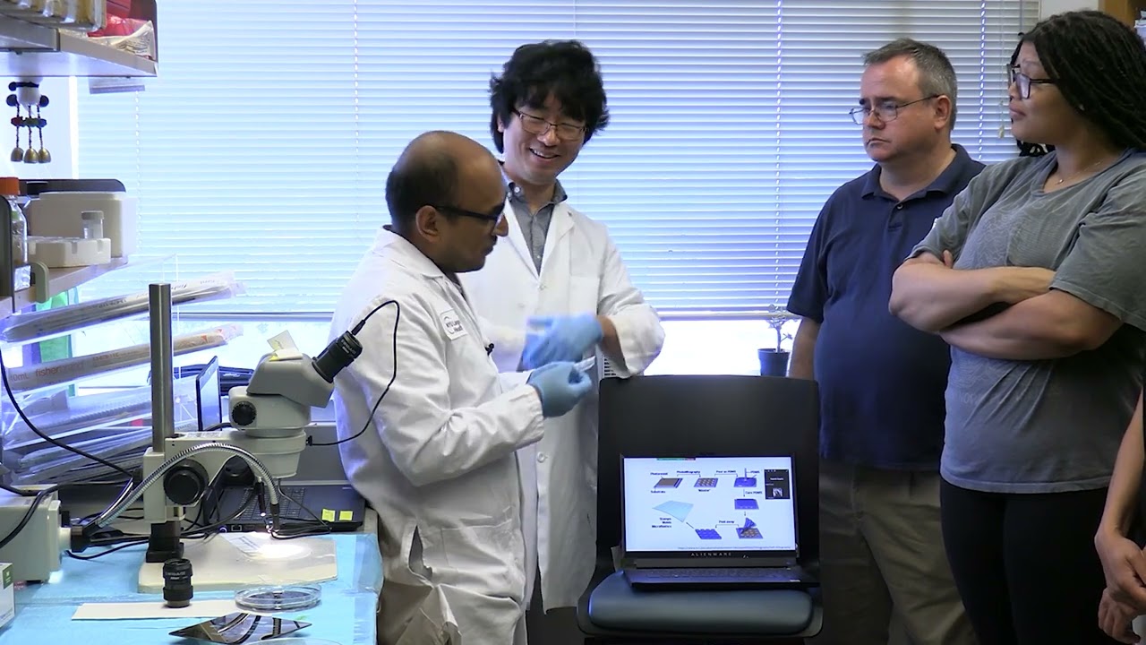
MechanoBio 101 for Teachers: Intro Soft Lithography and Microcontact Printing By Kapish Gupta
277
Soft lithography integrates physics, mathematics, and biology to create microscale patterns for biological applications. The process begins with photolithography: designing patterns in CAD software, printing onto chromium-coated masks, and exposing photoresist on silicon substrates using lasers. Positive/negative photoresist creates holes or pillars corresponding to mask patterns. PDMS (polydimethylsiloxane), a biocompatible polymer, is then cast from these masters. PDMS offers transparency for microscopy, gas permeability for cell culture, and easy sterilization via UV. The two-part polymer (A and B) must be mixed by weight in a standard 10:1 ratio, with bubbles removed through degassing under vacuum. After curing at elevated temperatures (60-80°C) for 1-2 hours, the solid elastomer can be peeled as a negative replica, ready for biological applications.
Click to watch →

Mod-01 Lec-16 Soft Lithography - I
2.5K
Soft lithography is a non-photolithographic patterning technique pioneered by George Whitesides' group at Harvard in the mid-1990s, which enables micro and nano fabrication through self-assembly and replica molding. Unlike photolithography, it can create both topographic structures and chemically patterned regions with different surface energies. The technique is particularly valuable for applications requiring large-area micro/nano structures such as sensors, biological applications, structural color, and textured hydrophobicity, where defect-free quality control is less stringent than in microelectronics. The molding group of soft lithography techniques, including replica molding (RM), MIMIC (Micro Molding in Capillaries), SAMIM (Solvent-Assisted Micro Molding), and CFL (Capillary Force Lithography), achieve pattern replication through capillary-driven flow of polymer solutions. Cross-linked PDMS (polydimethylsiloxane) is the most popular stamp material due to its unique properties: it is an inorganic polymer with a silicon-oxygen backbone, exhibits room temperature elasticity, is optically transparent, biocompatible, non-toxic, chemically resistant, and has low surface energy (approximately 20 mJ/m²). The curing process transforms a viscous liquid into an elastic elastomer through thermal treatment, with the cross-link density determined by the ratio of cross-linker to base polymer.
Click to watch →
Lec 20 Soft Lithography - I
1.4K
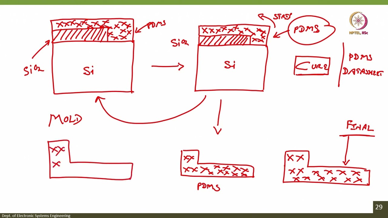
After stripping the photoresist with acetone, PDMS is poured over the patterned silicon dioxide mold and spin-coated to create a uniform thickness. The PDMS is then cured by heating at specified temperatures. Once cured, the PDMS replica is peeled off the mold, leaving behind the original silicon dioxide mold. The PDMS replica contains the exact inverse pattern of the mold, which can then be used as a stamp for further patterning operations.
Click to watch →

How to make PDMS devices
36.4K
PDMS (polydimethylsiloxane) is a versatile silicone elastomer used for creating microfluidic devices through soft lithography. The material consists of a base polymer and a curing agent that must be mixed in a precise 10:1 weight ratio. The base has a viscous honey-like consistency, while the curing agent is more fluid. Proper preparation requires accurate weighing, thorough mixing for at least one to two minutes, and degassing in a vacuum chamber to eliminate air bubbles that would compromise channel integrity. Understanding these fundamental properties and preparation steps is essential for successful microfluidic device fabrication.
Click to watch →

PDMS Tutorial
7K
This final section covers baking PDMS to achieve proper hardness. Check oven temperature (target 60°C, may vary 50-70°C) using a thermometer, then turn it off to conserve battery. Place samples in the oven and level them carefully using glass slides and a circular leveler—uneven samples create problematic slopes when cut. The leveler should always stay on top of the furnace. Close the door gently to avoid disturbing the level. PDMS cures at 60°C for approximately two days (or 24 hours). Longer curing times produce harder, less sticky PDMS; shorter times (as little as 30 minutes) produce softer, stickier material. Reference tables are available for specific hardness requirements.
Click to watch →
Deep Dive
Basic electrical circuit theory and micro-electrode design, specifically how metal deposition and patterning interface with fluidic channels.
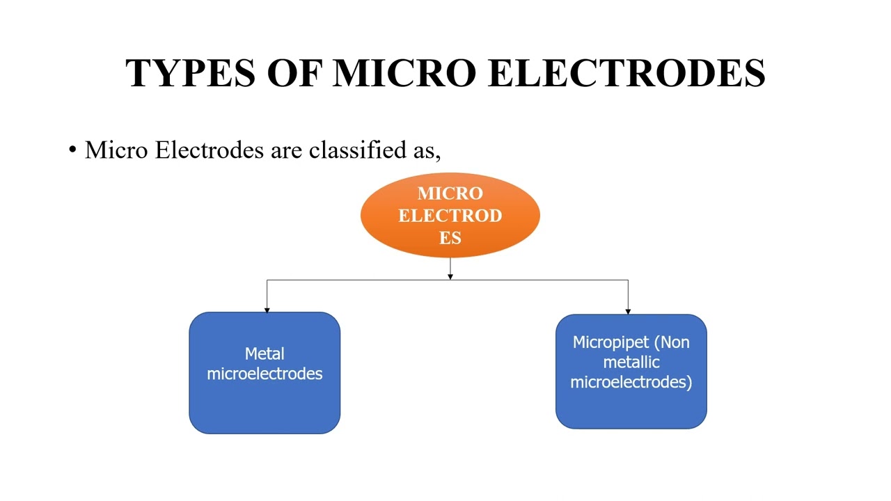
BASICS OF BIOMEDICAL INSTRUMENTATION - UNIT 1 - Micro Electrodes
2.4K
Non-metallic microelectrodes (micropipettes) are fabricated by heating and stretching glass capillaries to create fine tips (~1 micrometer). Glass serves dual purposes of mechanical support and insulation. The active tip contains metallic areas (silver solder alloy, platinum, or silver alloys) filled with 3M KCl electrolyte and sealed with metal electrodes (silver/AgCl, platinum, or stainless steel). The equivalent circuit includes metal-electrolyte interface components (RME, CME, EMA). Two key potentials exist: liquid junction potential (EJ) between pipette electrolyte and intracellular fluid, and potential (EP) from the glass membrane. All DC potentials combine in the source EM = EJ + EP + EMA - EMB, representing complete electrical behavior.
Click to watch →
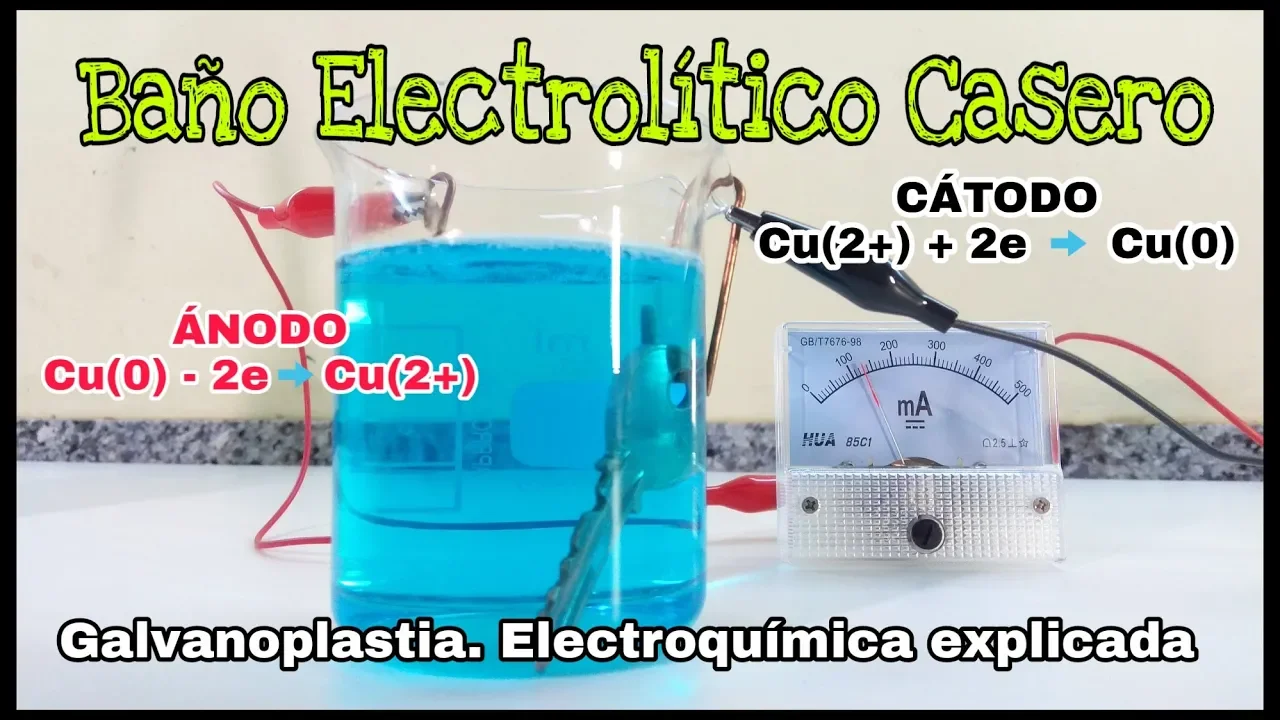
BAÑO ELECTROLÍTICO CASERO | GALVANOPLASTIA | ELECTROQUÍMICA EXPLICADA
180.8K
When current flows through the circuit, metal ions in the electrolyte migrate toward the cathode where they gain electrons and deposit as solid metal coating. Simultaneously, the anode releases metal ions into the solution as it oxidizes. The ammeter confirms current flow, demonstrating electron movement through the external circuit. Removing an electrode breaks the circuit and stops current flow. This bidirectional ion migration enables metal transfer from the anode to the cathode, with the deposited metal thickness depending on current strength and duration.
Click to watch →

Mod-01 Lec-11 Lecture-11
507
This section presents the theoretical framework for understanding electrochemical interfaces in microfluidics. At conducting phase interfaces, charge separation creates the electric double layer consisting of: (1) Charged electrode surface, (2) Water dielectric layer, (3) Counter ions forming the outer Helmholtz plane, (4) Diffuse layer extending into bulk solution. The Poisson-Boltzmann equation d²ψ/dx² = K²ψ describes potential distribution, with solution ψ(x) = A e^(-Kx) showing exponential decay. The charge density ρ = -4πDεK²A e^(-Kx) relates to surface charge density. This potential distribution drives electrokinetic flows in microchannels, enabling surface-driven fluid manipulation essential for bioMEMS devices.
Click to watch →

MOT 융합기술개론1 2026 류시형교수님 20260312
255
Micro-channel manufacturing creates tiny channels (10-100 micrometers) for microfluidic applications in biomedical devices, chemical reactors, and thermal management systems. Manufacturing techniques include photolithography, laser machining, and micro-milling. Electroless plating deposits metal onto substrates without external electrical current through chemical reduction, creating micro-parts and micro-features difficult to manufacture conventionally. This technique enables creation of micro-springs, micro-features on complex geometries, and surface modification of micro-parts for specialized applications.
Click to watch →
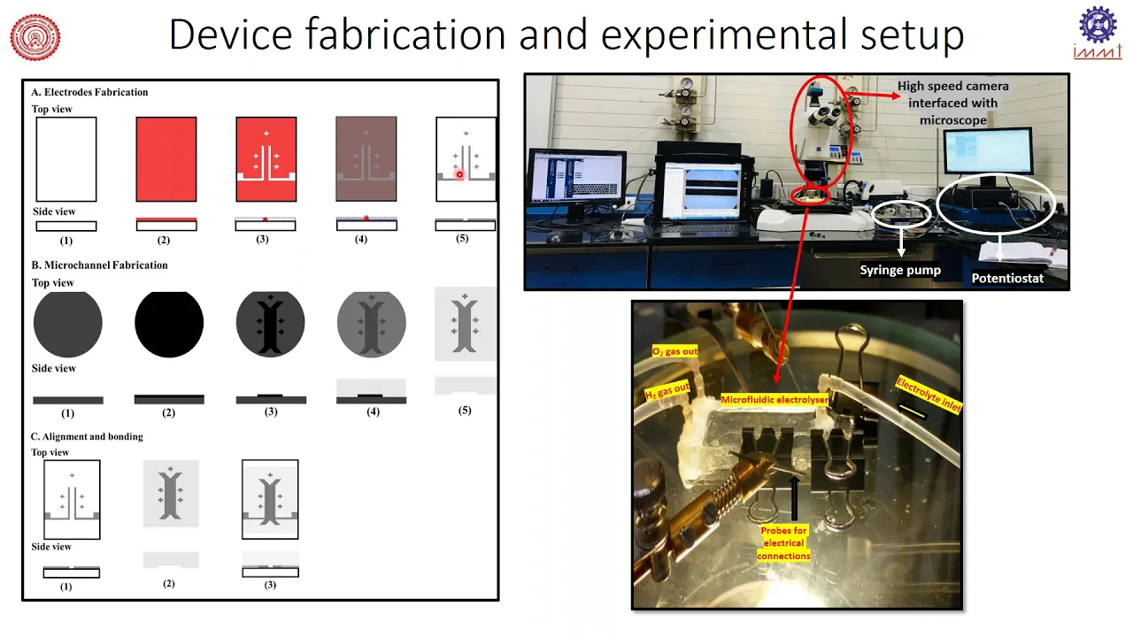
IIChE-MRC Diamond Jubilee Lecture Series (Lecture 2)
227
The microfluidic electrolyzer is fabricated using photolithography and sputtering techniques. A silicon wafer is coated with photoresist, exposed to UV radiation through a mask, and developed to create electrode patterns. Electrode materials (platinum for cathode, gold for anode) are deposited using sputtering. The microchannel is fabricated using negative photoresist (SU-8) and PDMS. The electrode layer and channel layer are aligned and bonded together. Laminar flow is verified using dye visualization, where colored dye does not mix with the colorless fluid, confirming no intermixing between different fluid streams.
Click to watch →
Deep Dive
Cleanroom safety protocols and standard operating procedures for handling hazardous chemicals and microfabrication equipment.
Lec 3: Fabrication Process - II
2K
This extensive section covers clean room operations essential for microfabrication. Topics include: (1) Wafer contamination sources—organic (skin oils, body fluids), metallic (sodium, potassium, heavy metals), native oxide (<10nm), and micro roughness requiring thorough cleaning; (2) Clean room classification by particle concentration: Class 1 (1 particle/cubic ft), Class 10, Class 100, etc., with HEPA filtration and controlled environmental parameters (temperature, humidity, sound, lighting); (3) Personnel protocols: gowning sequence (gloves → gown → hairnet → face mask), prohibited items (fur, jewelry), prohibited activities (eating, mobile phones), and communication restrictions; (4) Wet bench safety: acid-specific gloves, HF handling in Teflon containers, fume hood requirements, proper chemical mixing (acid to water), MSDS consultation; (5) Emergency response: spill procedures (flush skin immediately), disposal protocols, and first aid availability.
Click to watch →

UIUC MRL MicroFab cleanroom walkthrough training video
807
This comprehensive training video covers the essential safety protocols, equipment operation procedures, and workflow standards for the MicroFab cleanroom at UIUC MRL, including gowning procedures, proper use of fume hoods for spin coating and developing processes, chemical handling and disposal protocols, and emergency response procedures across four specialized fabrication bays.
Click to watch →

Clean Room | classification | Semiconductor Manufacturing| VLSI | Fabrication| Microelectronics | ME
751
Clean rooms require comprehensive safety infrastructure beyond contamination control. Hazardous chemicals (HF, HCl, H2SO4) require specific PPE and handling procedures. Toxic gases (arsine, silane) need gas cabinets, leak detectors, and emergency shut-off systems. High voltage equipment mandates lockout/tagout protocols. Emergency infrastructure includes accessible showers/eyewash stations, fire suppression using inert gases (not water), and continuous gas detection systems. Regular safety drills ensure rapid response. Contamination monitoring uses real-time particle counters with immediate alerts, surface swabs for microbial testing, and comprehensive logging of all activities from maintenance to cleaning schedules. Scheduled deep cleaning maintains designated cleanliness classes. This integrated approach protects both product integrity and worker safety.
Click to watch →

CLEANROOM GOOD MANUFACTURING PROCESSES
861
Cleanrooms are controlled environments that limit air particle concentration to prevent product contamination; workers must wear appropriate PPE including cleanroom suits, gowns, aprons, hair/beard nets, gloves, eye protection, and non-porous closed-toed shoes, while following strict chemical handling procedures such as wearing goggles and gloves, consulting Safety Data Sheets (SDS), and avoiding acid spills on container exteriors.
Click to watch →

UIUC MRL Cleanroom Orientation
610
The UIUC MicroFab cleanroom provides micro and nano-fabrication facilities with four specialized bays (optical lithography, sample cleaning, metal etching, and acid etching), requiring users to complete safety training, wear appropriate PPE including cleanroom gown, shoe covers, gloves, and mask cover, follow specific procedures for chemical handling and waste disposal, and work with at least one other person for safety; the cleanroom operates 24/7 except for cleaning hours, and users must log in/out on computers to track work time for billing purposes.
Click to watch →
Prerequisite Knowledge
- Concept 01Fundamental principles of photolithography, including the role of photoresists, UV exposure mask alignment, and chemical developing.
- Concept 02Material properties of Polydimethylsiloxane (PDMS), particularly its curing process, biocompatibility, and optical transparency in soft lithography.
- Concept 03Basic electrical circuit theory and micro-electrode design, specifically how metal deposition and patterning interface with fluidic channels.
- Concept 04Cleanroom safety protocols and standard operating procedures for handling hazardous chemicals and microfabrication equipment.
Subsequent Learning
- Step 01Application of integrated devices in Lab-on-a-Chip (LoC) and Organ-on-a-Chip (OoC) technologies for biomedical research.
- Step 02Advanced electrokinetic techniques, such as dielectrophoresis (DEP) and electroosmotic flow, for active particle and fluid manipulation.
- Step 03Integration of electrochemical and impedance-based biosensors for real-time molecular and cellular sensing.
- Step 04Exploration of high-throughput manufacturing alternatives to photolithography, such as injection molding, 3D printing, and roll-to-roll fabrication.
PDMS Device Build
Cleanroom Coating
UV Patterning
PDMS Sealing
Device Finalization
PDMS Device Build
0:07Playing Section
- 1
Introduces multi-layer microfluidic device integrating electrical circuits on a glass slide.
- 2
Explains need for patterned aluminum under PDMS to create electric fields in channels.
- 3
Starts fabrication with elastomer mixture at a 10:1 base-to-curing-agent ratio.
Thermoplastic Microfluidics and 3D Printing: Alternatives to PDMS and Photolithography
While polydimethylsiloxane (PDMS) and photolithography are standards for academic prototyping, they face significant criticism regarding scalability, cost, and material limitations. PDMS is highly permeable and prone to absorbing small hydrophobic molecules, which can bias biochemical assays and drug-screening results. Furthermore, the manual, labor-intensive nature of soft lithography makes it unsuitable for industrial-scale mass production. An increasingly dominant alternative is the use of thermoplastics (such as Cyclic Olefin Copolymer, PMMA, and polystyrene) paired with fabrication techniques like injection molding, hot embossing, or high-resolution 3D printing. Thermoplastics do not absorb small molecules, offer superior chemical resistance, and are highly compatible with high-throughput commercial manufacturing. Additionally, 3D printing bypasses the need for expensive cleanroom environments and photolithographic masks altogether, allowing for rapid, low-cost, and truly three-dimensional prototyping. Introducing students to these alternatives provides a realistic understanding of what is required to transition microfluidic designs from academic labs to commercial medical and diagnostic devices.
Deep Dive
Application of integrated devices in Lab-on-a-Chip (LoC) and Organ-on-a-Chip (OoC) technologies for biomedical research.

NanoBiotech Laboratory, Dept of Bio and Brain Eng, KAIST (바이오및뇌공학과 나노바이오공학 연구실)
247
This video introduces microfluidic lab-on-a-chip technology developed at KAIST, which integrates biological sample pre-processing and detection into miniature devices for life science, chemistry, medicine, and environmental applications. Key innovations include point-of-need testing (Poc) for immediate diagnostics, finger-force microfluidic control eliminating external equipment, and digital PCR systems for genetic analysis. The research extends to organ-on-a-chip technology using 3D cell culture to model vascular occlusion, intestinal inflammation, and hepatic metabolism. Spheroid array technology enables high-throughput analysis of cellular responses. These platforms aim to replace animal testing, accelerate drug development by evaluating safety and efficacy, and provide more accurate human-relevant disease models for pharmaceutical research.
Click to watch →

Chips fazendo papel de órgãos: o futuro da medicina!
47.2K
Organ-on-a-chip technology is a miniaturized mechanical structure that uses microfluidic chips to replicate human organ functions in laboratory settings, enabling more accurate drug testing and treatment development while reducing reliance on animal models; this technology, developed at Harvard and studied in Brazil by researchers like Suélia Fleury from the University of Brasília's Biomedical Engineering Group, is being applied to test products like the Rafa wound healing treatment for diabetic foot ulcers, which combines natural latex with photobiostimulation to promote blood vessel growth and tissue regeneration.
Click to watch →
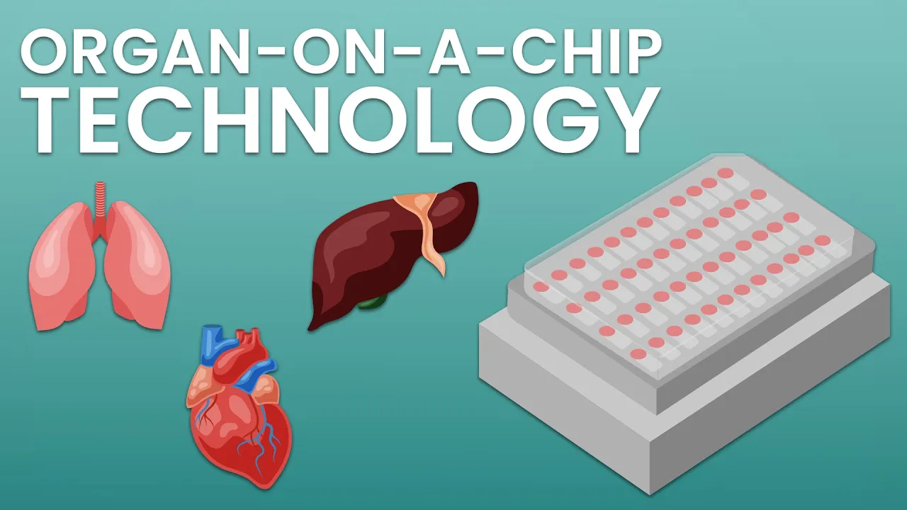
What is organ-on-a-chip technology?
46.6K
Organ-on-a-chip (OOC) technology uses microfluidic chips with extracellular matrix-coated scaffolds to culture primary human cells, enabling the formation of physiologically relevant organ or tissue replicas that mimic human biology; this technology bridges the gap between traditional 2D cell culture and animal models by providing more accurate predictions of drug effects, toxicity, and disease mechanisms, supporting the development of safer and more effective therapeutics including next-generation therapies like oligonucleotides, antibodies, and cell/gene therapies.
Click to watch →

El Fin de la Experimentación Animal
109.1K
Organ-on-a-chip technology has diverse applications in biomedical research. For example, a heart-on-a-chip can predict how a drug will affect heart rhythm, while a liver-on-a-chip can evaluate hepatic toxicity. This technology is particularly useful for researching diseases like cancer and cardiovascular diseases. Multiple chips can be connected to study how organs interact with each other. The technology enables more precise observation of how cells interact with substances like toxins or medications, and can be used to personalize treatments for individual patients by testing different therapies in laboratory conditions before clinical application.
Click to watch →

LessON: Что такое орган-на-чипе?
117
Organ-on-a-chip is an innovative biomedicine technology consisting of devices approximately the size of a USB drive that imitate human organ structure and function. These devices contain microchannels and chambers populated with living human cells through which nutrient medium flows to simulate blood circulation. The technology reproduces key physiological conditions including controlled nutrient flow, intercellular interactions in three-dimensional space, and dynamic processes like respiratory movements, cardiac contractions, and intestinal peristalsis. This technology addresses three major problems: the 90% failure rate of drugs in human clinical trials due to species differences, limitations of traditional two-dimensional cell cultures, and ethical concerns of animal testing. The 2023 FDA Modernization Law approved alternative methodologies, with the first liver-on-a-chip application accepted in 2024. Main applications include preclinical research, toxicological testing, academic disease research, and personalized medicine. Specific organ models include lung-on-a-chip for respiratory diseases, liver-on-a-chip for hepatotoxicity and drug metabolism, gut-on-a-chip for absorption and inflammatory diseases, and placenta-on-a-chip for pregnancy complications.
Click to watch →
Deep Dive
Advanced electrokinetic techniques, such as dielectrophoresis (DEP) and electroosmotic flow, for active particle and fluid manipulation.
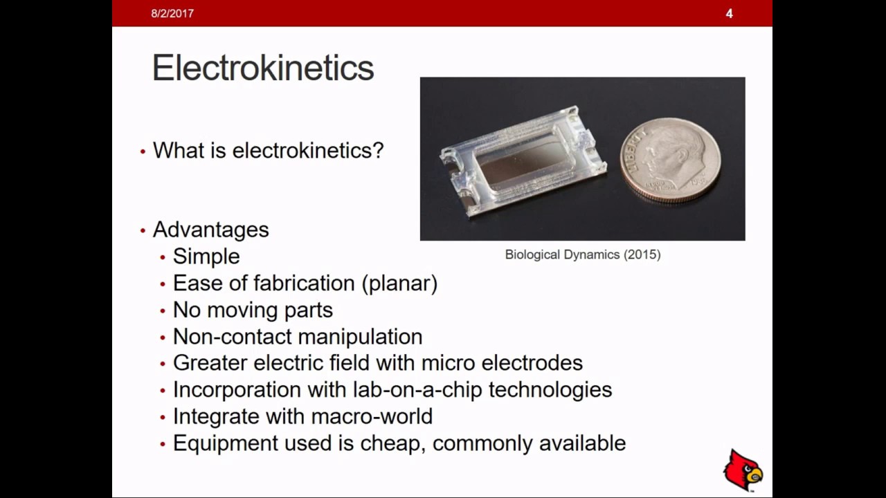
Introduction to Dielectrophoresis (DEP)
10.2K
Dielectrophoresis (DEP) is a technique that manipulates particles using non-uniform electric fields by inducing dipoles in particles based on their dielectric properties relative to the surrounding medium; the Clausius-Mossotti factor determines whether particles experience positive DEP (attracted to high-field regions) or negative DEP (repelled from high-field regions), enabling applications in cell separation, particle sorting, and manipulation in microfluidic devices.
Click to watch →

Mod-01 Lec-18 Electrokinetics
686
The dielectrophoretic force is F_DEP = 2π ε₁ K_CM a³ ∇(E₀²), where K_CM = (ε₂-ε₁)/(ε₂+2ε₁). Key dependencies: (1) Proportional to a³ (third power of size), (2) Depends on field gradient squared, (3) Independent of electric field sign, (4) Sign depends on K_CM. Since F_DEP ∝ a³, larger particles experience stronger forces than smaller ones. In microfluidic channels with electric field gradients, larger particles move toward regions of higher field intensity while smaller particles remain relatively stationary, enabling size-based separation of cells and particles. The DEP force direction depends on the Clausius-Mossotti factor sign. For particle trapping toward an electrode, F_DEP must be positive, requiring ε₂ > ε₁ (particle more dielectric than fluid). In microfluidic channels with asymmetric electrodes (hemispherical bottom, flat top), particles experience competing forces: DEP force (pulling toward electrode) and drag force (carrying with flow). For trapping to occur, F_DEP must exceed F_drag. The velocity profile in parallel-plate channels is parabolic: u(z) = (6u_avg/H²) z(H-z), where u_avg is average velocity.
Click to watch →

COMSOL's Hands-on Workshop on Microfluidic Devices @ NNIN/C, UMich
46.3K
Dielectrophoresis manipulates particles using non-uniform electric fields based on differences in polarizability between particles and surrounding medium. Particles experience forces proportional to the gradient of the square of the electric field. Positive dielectrophoretic (p-DEP) particles move toward high-field regions, while negative dielectrophoretic (n-DEP) particles move toward low-field regions. The force magnitude depends on particle shape, conductivity, permittivity, and field gradients. COMSOL implements dielectrophoresis through particle tracing physics combined with AC/DC electromagnetics, enabling separation of particles with different electrical properties for bioseparation and cell manipulation applications.
Click to watch →

Mod-23 Lec-23 Dielectrophoresis
5.1K
Dielectrophoresis is an electrokinetic phenomenon that enables the manipulation of neutral particles (with zero net charge) by applying a non-uniform electric field, where the dielectrophoretic force F_DP = P · ∇E acts on particles based on their electric dipole moment P and the spatial gradient of the electric field ∇E; unlike electrophoresis which relies on net particle charge, dielectrophoresis exploits the polarization properties of particles relative to their surrounding medium, making it particularly useful for separating and trapping biological cells and particles without requiring them to carry a net electrical charge.
Click to watch →

C. C. Mei Distinguished Speaker Series Spring 2018: Prof. Nadine Aubry
643
This section introduces fundamental principles of particle manipulation in microfluidic systems. Electrophoresis moves charged particles in DC fields proportional to charge and field strength, while dielectrophoresis moves neutral particles in nonuniform fields proportional to dipole moment and electric field gradient squared. The Clausius-Mossotti factor (beta) determines particle response: positive beta moves particles to high-field regions, negative beta to low-field regions. This enables particle separation based on dielectric properties and contactless trapping at channel centers. Multiple particles experience electrostatic interactions causing chaining phenomena where particles form elongated chains along walls. The point-dipole approximation treats particles as point dipoles, valid when particles are much smaller than channel dimensions. The Maxwell stress tensor approach accounts for field deformation by particles, necessary for larger particles.
Click to watch →
Deep Dive
Integration of electrochemical and impedance-based biosensors for real-time molecular and cellular sensing.
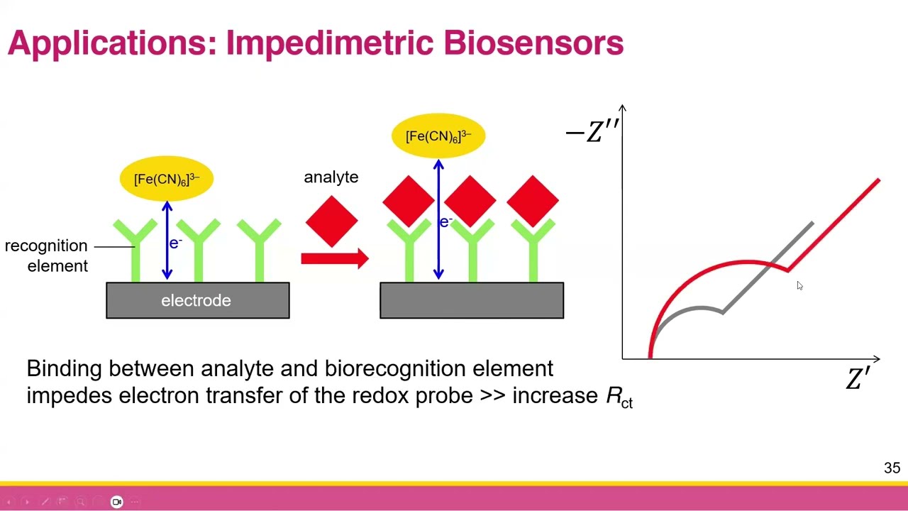
EP. 5 Basic Applications of EIS in Chemistry | EIS for Chemists: The Basics (ไทย)
783
EIS measurements are sensitive to electrode geometry, particularly the distance between working and counter electrodes. Increasing spacer length raises uncompensated solution resistance, which affects observed Rct values even with identical electrode materials. Beyond material characterization, EIS enables development of impedimetric biosensors for detecting specific analytes. These biosensors use recognition elements (like antibodies) that bind target molecules, creating barriers that increase Rct. The change in Rct correlates with analyte concentration, enabling quantitative detection. This principle has been applied to detect viral proteins, where Rct increases proportionally with viral concentration, producing linear calibration curves for sensitive biosensing applications.
Click to watch →
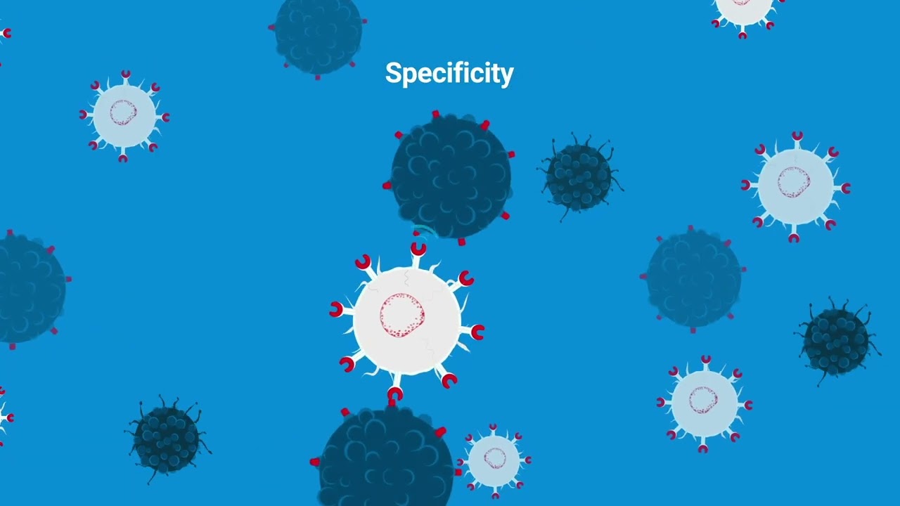
xCELLigence RTCA esight
236
The Agilent xCELLigence RTCA esight platform employs impedance-based label-free biosensor technology to enable real-time, automated cell analysis, allowing researchers to monitor cellular events such as cell death, adhesion, and morphology changes continuously without requiring fluorescent labels or endpoint measurements, thereby significantly reducing experimental time while providing comprehensive kinetic data for applications in immunotherapy and drug discovery.
Click to watch →
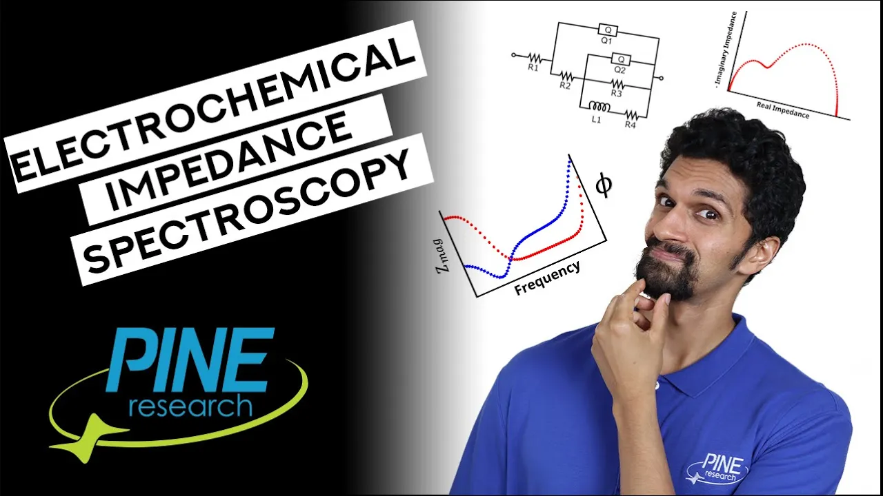
What is Electrochemical Impedance Spectroscopy (EIS) and How Does it Work?
151.7K
Electrochemical Impedance Spectroscopy (EIS) is a technique where a potentiostat applies a sinusoidal potential or current to an electrochemical system and measures the corresponding sinusoidal current or potential response; the technique uses Fourier transform to convert time-domain data to frequency-domain data, calculating impedance (the AC equivalent of resistance) from the ratio of potential and current amplitudes, along with phase shifts, which are then plotted as Bode plots (magnitude and phase vs. frequency) or Nyquist plots (real vs. imaginary impedance), allowing researchers to deconvolute different electrochemical phenomena occurring at characteristic frequencies (such as double-layer charging, solution resistance, charge transfer resistance, and molecular diffusion) that occur simultaneously but on different timescales, enabling both qualitative and quantitative analysis of electrochemical systems through equivalent circuit modeling.
Click to watch →

Ashley Chapin - “Hybrid Platform Development for In Situ Monitoring of the Gut-Brain-Axis” | MAMNA
158
Electrochemistry offers versatile real-time detection of molecules released from living cells without chemical pre-treatments or labeling. Using carbon fiber electrodes held at oxidizing potentials above serotonin's redox potential, researchers observe current spikes corresponding to serotonin release. Concentrations range from sub-micromolar to tens of micromolars, with release events occurring once per second or at varying frequencies depending on stimulation. However, traditional approaches only measure serotonin from the apical (top) side of gut epithelium, whereas the basolateral (bottom) side releases serotonin that stimulates enteric nerves. Gut-on-chip platforms provide convenient access to the basolateral surface. The developed platform integrates electrochemical impedance spectroscopy (EIS) on the top membrane surface to monitor cell coverage by detecting changes in electrical properties as cells attach, combined with cyclic voltammetry electrodes on the bottom surface for serotonin detection, enabling simultaneous physical and molecular monitoring.
Click to watch →

Introduction to Electroanalytical Techniques: Voltammetry, Potentiometry, Amperometry, EIS.
14.3K
Electrochemical impedance spectroscopy models electrode surfaces using equivalent circuits containing solution resistance, double-layer capacitance, and charge transfer resistance. At low frequencies, current flows through solution resistance and capacitive elements; at high frequencies, current preferentially flows through capacitors. Intermediate frequencies reveal contributions from both. Software analyzes impedance data across frequency ranges to determine equivalent circuit parameters. Charge transfer resistance changes proportionally to molecular binding extent, enabling quantitative detection of biomolecules. Carbon electrodes with pyrene NHS coupling chemistry provide cost-effective alternatives to gold electrodes for immunosensor development.
Click to watch →
Deep Dive
Exploration of high-throughput manufacturing alternatives to photolithography, such as injection molding, 3D printing, and roll-to-roll fabrication.

Enabling Paper-Like Displays: Roll-to-Roll Manufacturing
4.1K
Roll-to-roll manufacturing represents a fundamental paradigm shift from conventional batch processing in display manufacturing. Unlike Gen 10 glass facilities costing billions, roll-to-roll uses printing-press-like continuous web handling. The key challenge is adapting photolithography to flexible plastic substrates that deform by hundreds of parts per million. HP's approach involved starting fresh without legacy glass-processing assumptions, leading to imprint lithography as the enabling technology. Imprint lithography solves alignment problems by encoding all patterning information into a single monolithic 3D stamp molded at the beginning of the process, eliminating multiple photolithography steps. This achieves 40nm resolution on 50-micron plastic at 5m/min throughput. Sustainability benefits include reduced mass (plastic weighs 50x less than glass), lower temperatures, and compact equipment. The zeroth-order sustainability rule states that reducing mass proportionally reduces energy consumption. Cleanroom requirements are dramatically reduced to localized environments. Equipment cost comparisons show roll-to-roll achieves approximately order-of-magnitude cost reductions compared to conventional photolithography.
Click to watch →

Revell Just Showed Airfix How It’s Done - Tuesday Talk 11-08-26
1.5K
Injection molding imposes constraints including the need for draft angles and the inability to create undercuts without expensive slide molds. Small, thin parts may appear strange on computer screens but become acceptable when manufactured. 3D printing offers an alternative for complex components with undercuts, allowing companies to provide data for customers to print their own versions. This approach requires additional design work to remove undercut sections but provides more flexibility and can reduce costs for certain parts.
Click to watch →

3D Mastering for Nanoimprint and Injection Molding
787
Master durability improves through metallic conversion: template stripping deposits thick metal layers (750 nm silver) then mechanically strips away the film; electroplating coats patterns with seed layers and plates metals (nickel, gold, copper) to desired thicknesses. Both methods preserve dimensional accuracy, enabling long-lasting masters for industrial replication. Injection molding transforms nanoimprint masters into precision plastic parts at industrial scale, producing tens to hundreds of thousands of units daily. Current patterning speed is ~1,000 square microns per minute, comparable to electron beam lithography. Future developments include multi-tip arrays (10-tip linear arrays, commercial availability planned), 8-inch wafer-capable systems, high-speed laser systems for interconnects, and fully automated platforms with tip/sample exchange modules to enable large-scale manufacturing adoption.
Click to watch →

LE NUOVE TECNOLOGIE DI STAMPA 3D INDUSTRIALE e ONLINE
85.4K
3D printing and injection molding have different economic and practical advantages. Injection molding requires expensive molds (costing significant money) and minimum production runs to be economical. Mold design errors require complete remaking. 3D printing eliminates mold costs entirely, allows design changes without remaking, and provides faster turnaround times. For certain production volumes and object types, 3D printing can be more advantageous in terms of time, practicality, and design flexibility, though it may not completely replace injection molding for all applications.
Click to watch →
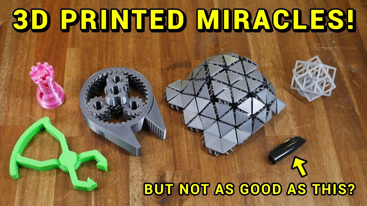
Why 3D printing is amazing! (but will not replace industry manufacturing)
163.6K
This video explains why 3D printing is amazing but will likely never replace injection molding for mass production. While hobby 3D printers have become more affordable and capable than ever before, making it easier for individuals to create objects from their ideas, the existing manufacturing process of injection molding remains superior for high-volume production due to its monstrous efficiency.
Click to watch →
PDMS Device Build
Cleanroom Coating
UV Patterning
PDMS Sealing
Device Finalization
PDMS Device Build
0:07- 1
Introduces multi-layer microfluidic device integrating electrical circuits on a glass slide.
- 2
Explains need for patterned aluminum under PDMS to create electric fields in channels.
- 3
Starts fabrication with elastomer mixture at a 10:1 base-to-curing-agent ratio.
Thermoplastic Microfluidics and 3D Printing: Alternatives to PDMS and Photolithography
While polydimethylsiloxane (PDMS) and photolithography are standards for academic prototyping, they face significant criticism regarding scalability, cost, and material limitations. PDMS is highly permeable and prone to absorbing small hydrophobic molecules, which can bias biochemical assays and drug-screening results. Furthermore, the manual, labor-intensive nature of soft lithography makes it unsuitable for industrial-scale mass production. An increasingly dominant alternative is the use of thermoplastics (such as Cyclic Olefin Copolymer, PMMA, and polystyrene) paired with fabrication techniques like injection molding, hot embossing, or high-resolution 3D printing. Thermoplastics do not absorb small molecules, offer superior chemical resistance, and are highly compatible with high-throughput commercial manufacturing. Additionally, 3D printing bypasses the need for expensive cleanroom environments and photolithographic masks altogether, allowing for rapid, low-cost, and truly three-dimensional prototyping. Introducing students to these alternatives provides a realistic understanding of what is required to transition microfluidic designs from academic labs to commercial medical and diagnostic devices.
Fundamental principles of photolithography, including the role of photoresists, UV exposure mask alignment, and chemical developing.
Material properties of Polydimethylsiloxane (PDMS), particularly its curing process, biocompatibility, and optical transparency in soft lithography.
Basic electrical circuit theory and micro-electrode design, specifically how metal deposition and patterning interface with fluidic channels.
Cleanroom safety protocols and standard operating procedures for handling hazardous chemicals and microfabrication equipment.
Application of integrated devices in Lab-on-a-Chip (LoC) and Organ-on-a-Chip (OoC) technologies for biomedical research.
Advanced electrokinetic techniques, such as dielectrophoresis (DEP) and electroosmotic flow, for active particle and fluid manipulation.
Integration of electrochemical and impedance-based biosensors for real-time molecular and cellular sensing.
Exploration of high-throughput manufacturing alternatives to photolithography, such as injection molding, 3D printing, and roll-to-roll fabrication.
18.6K views258likes11:45@microfluidicsandmultiphase8434Original Release: 2016-08-31
hello everyone welcome to the microfluidics and multiface flow laboratory youtube channel in this video i would like to show a fabrication process of a pdms microfluidic device integrated with an electrical circuit this device is consisted of multiple layers in order to create electric fields at specific points of interest inside our micro channels we need to pattern a circuit on a glass slide beneath the pdms block therefore we use an aluminum coated glass slide that undergoes a photolithography process the desired circuit is patterned by uv light and etched away by the remover then the whole glass surface is covered by a thin layer of pdms ultimately the pdms micro channel blog binds irreversibly on top we're now in the transport science core of the watson school at binghamton university the first step of fabrication process is to prepare the elastomer which is a mixture of pdms pre-polymer base and a curing agent at the weight ratio of 10 to 1.
now we are in the clean room to pattern the electrical circuit on this aluminum coated glass slide the first step is to put on a thin layer of primer which prepares the surface for spin coating the positive photoresist s1813 on top of it so me after spin coating the photoresist on the glass slides we need to soft break them at 95 degrees for one minute now that we have a thin layer of positive photoresist based on the aluminum coated glass slide we pattern our circuit design using the mask aligner here we have this photo mask of our design placed on two glass slides which are going to be exposed to the uv light after the mask alignment we need to post make the glass slide at 95 degrees celsius for one minute then we will immerse it in remover pg to etch away the aluminum layer so after the cleaning process to remove the photoresist residue from the glass slide we spin coat a thin layer of pdms that we had prepared earlier and then we let it cure on the hot plate now we use the su-8 mode that we have designed and fabricated earlier the full procedure is shown in a video by lilu on our youtube channel now the marker channel block is irreversibly bonded to the glass slide finally the last step would be to peel off the pdms layer from the terminals and attach the wiring using conductive epoxy and now the epoxy is cured and the device is ready for use thank you for watching this video you
Up Next

27:48
Legal Pluralism: Theory, Phases & Living Law Explained
@AakashSinghRathore
5.1K views•2017-08-21

12:54
Triumph of Orthodoxy Icon: Byzantine Art & History Explained
@BenCallan
2.1K views•2024-08-06

9:49
FastAPI vs Flask vs Django: Choosing the Right Python Web Framework
@TechWithTim
302.5K views•2024-05-26

1:42
Game of Thrones Opening Credits: A Cinematic Analysis
@gameofthrones
46.3M views•2011-04-18
Related Study Plans & Knowledge Roadmaps
Structured learning paths in General & Interdisciplinary Studies
general-studies
Elevator Engineering: History, Physics & Cities
01From Hoists to Safety Brakes: The Dawn of Vertical Lift
02Hydraulic vs. Traction: The Engineering Physics of Elevators
03Modern Speed, Safety, and Algorithms
+ 2 more learning modules
12h5 modules
Explore Roadmap
general-studies
Rubber: Material Science, History & Geopolitics
01Origins of Natural Rubber & Mesoamerican History
02The Chemistry of Natural Rubber & Vulcanization
03The Geopolitics of the Rubber Boom & Colonization
+ 2 more learning modules
12h5 modules
Explore Roadmap
general-studies
Containerization: Evolution, Logistics & Trade
01Ancient Trade & Bulk Cargo: Amphorae to Barrels
02The Industrial Revolution & Cardboard Packaging
03The Containerization Revolution: Malcom McLean
+ 2 more learning modules
12h5 modules
Explore Roadmap
general-studies
Textile Tech: Evolution, Labor & Global Impact
01Pre-Industrial Textiles: Handloom & Cottage Industry
02Mechanization: The Spinning Jenny to the Power Loom
03The Factory System & Global Labor Transformation
+ 2 more learning modules
10h5 modules
Explore Roadmap