













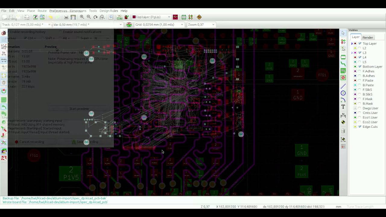



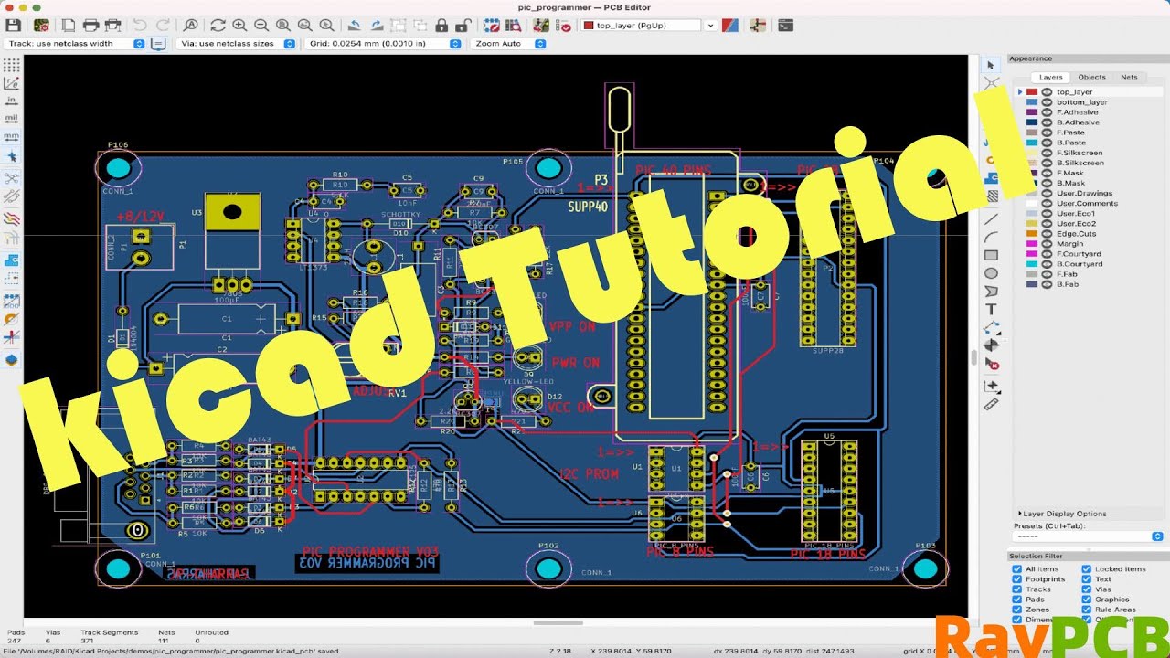






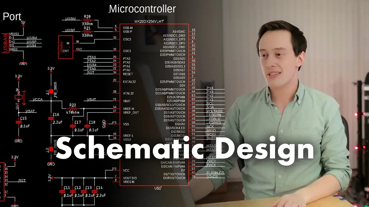




KiCad is a free open-source EDA suite that enables users to design circuit boards through a systematic workflow: first creating schematics using the schematic editor with keyboard shortcuts (A=add, R=rotate, V=value, X/Y=flip), then assigning component footprints and running electrical rules checks (ERC), followed by PCB layout using the PCB editor with routing keys (R=rotate, F=flip, X=route traces, M=align to pads), setting design rules, adding copper pours and ground planes, performing iterative layout improvements, and finally generating Gerber files for manufacturing through the CAM processor.
KiCad PCB Design: Schematic to Gerber Workflow Guide
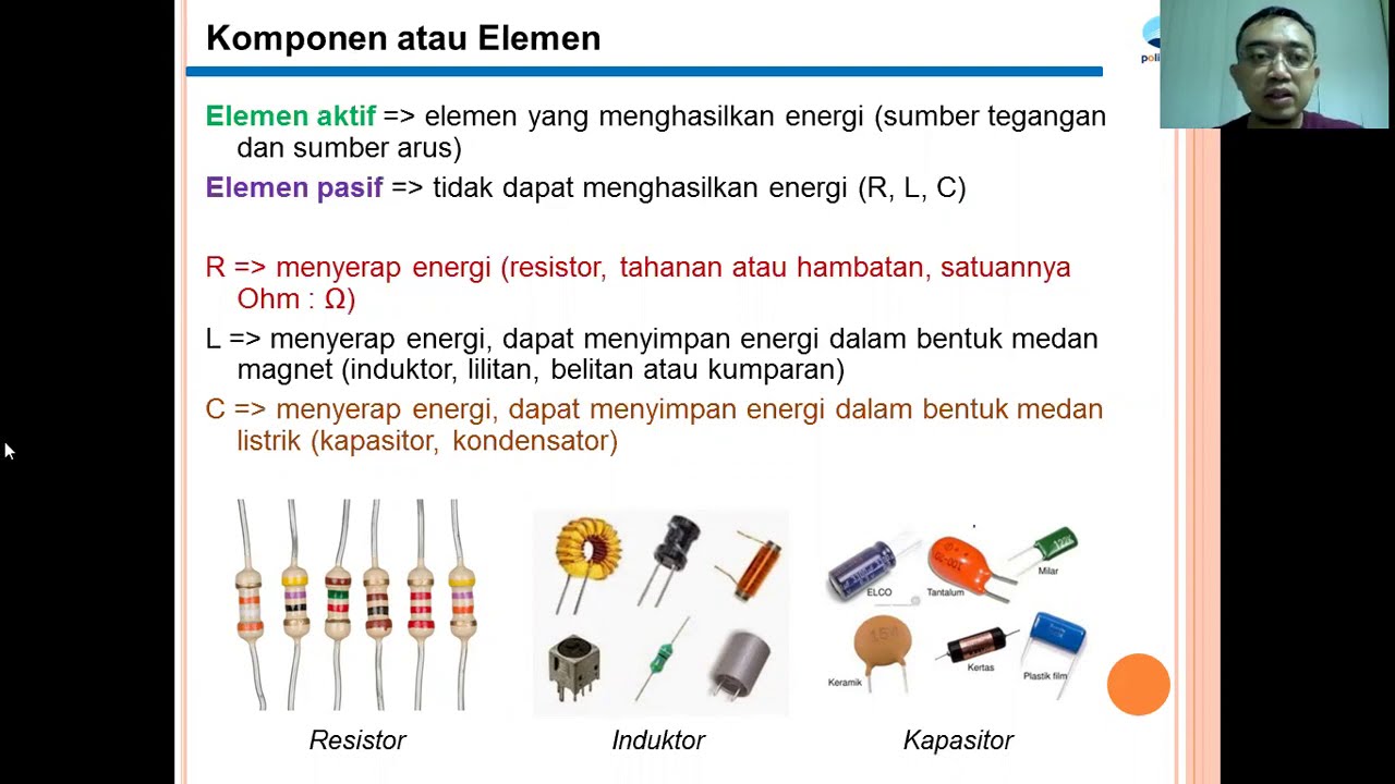
Added:Basic electrical circuit theory, including how components like resistors, capacitors, and integrated circuits interact in a schematic.
The conceptual difference between a schematic symbol (logical representation) and a PCB footprint (physical layout).
Fundamental anatomy of a Printed Circuit Board (PCB), including traces, copper layers, solder masks, silkscreen, and vias.
Familiarity with basic software navigation and file management within a computer-aided design (CAD) environment.
Advanced routing techniques, such as differential pair routing, length matching, and high-speed signal propagation.
Multi-layer PCB design strategies, including layer stackup configuration, ground planes, and power plane segmentation.
Design for Manufacturing (DFM) and Design for Assembly (DFA) guidelines to ensure error-free physical fabrication.
Custom library management, including creating proprietary schematic symbols and footprints with integrated 3D models.
Electromagnetic Compatibility (EMC) and signal integrity fundamentals to minimize noise and interference in high-frequency designs.
91.7K views1.7Klikes49:56Original Release: 2022-01-17
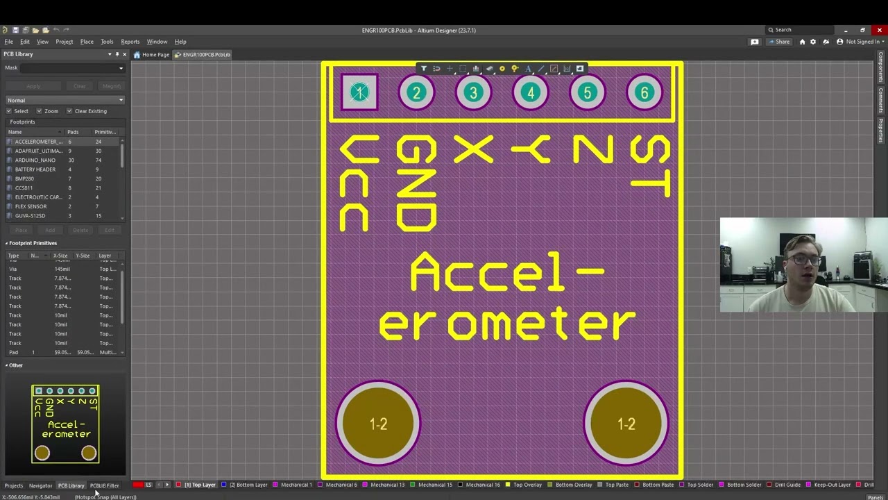
hi this video covers my experiences with free open source software called kycad to draw circuit diagrams and create printed circuit board layouts I'm assuming no prior knowledge of keycard for anyone to watch through this there was an index to the video so you don't have to fuff around with watching hourong videos for no reason you can jump to the bits you're interested in you can download and install key CAD onto your PC from the key cad.org website when you launch kead this is the main control panel and on the right hand side here's the pallet of the different applications that you can launch and on the left hand side is a view of the files of your project so you can go to file new project and create one there and of these applications here really you need to be familiar with at least the most important ones the top four ones here but actually the fifth one is useful too and that's important as well unless you're going to be using some external Gerber viewer because there are many third party ones and you might have a favorite one anyway for now is if you create a project and then you can launch the schematic editor so working top down basically when you launch the schematic editor comes up like this first off I strongly recommend you examine the preferences here because it's possible to make life a lot more comfortable if you're coming from using a different CAD package in my case I was migrating from Eagle Cad and the transition was made easier by going to the mouse settings here then setting things up as shown here with these boxes unchecked Zoom speed setting set to low and then the left Mouse button was set to this drag any object settings also under display options here I set the grid to lines mode if you wanted you could also create your own color theme here as well I created one here okay back to the schematic editor you can turn the Grid on or off by just clicking here if you want to and really this is quite easy to use you use a key press the A Button uh for adding a component R for rotating it V to select a value for the component like 10K 20K for a resistor or whatever and you can hit escape to back out and you can also use the usual control key combinations like copy paste undo a standard you know control X Etc and you can press the x or y button to flip a component along the x or the y direction and that's it really those are the most important ones but you can also always just check by clicking on list hot keys and see the letter assigned to different command if you if you want to just check there but anyway yeah so once you're here just hit the a key and the the first time you do that it might take a little while to bring up um this list of symbols these are different libraries of uh components that are available the main important ones here are power and device so you always need a ground symbol and a power symbol so you can just go into power here and pick the symbol that you want and device will contain things like resistors and capacitors so again that's pretty fundamental there it is here so you can see the types of things are here if you don't often you won't need to do that though you can just type here so if you want to draw in a resistor then you can just type resistor here and it finds it here there's a resistor you can just double click that and then start positioning that somewhere and then hit Escape if you want to and then you could then start drawing y's to it by just hovering over here and then you can just start making connections I'm just going to hit Escape there and press a again to add another component and this time I'm going to go to the power section so let me just close device because I want to put a plus 3.3 symbol can find one here that'll do fine and I can either directly connect it or just put it here and because I'm still in the ad mode cuz I'm not hit Escape if I just click anywhere then come back to here and I can pick another one so if I just scroll down I'm just using a center Mouse thing to do this so scroll down to a ground symbol okay that and then put that somewhere like that and then I can just hover over there left Mouse click oh um I'm still in the symbol editor mode so if I hit escape and hit escape again now I'm out of there so now I can just click and then that's done all right and like I mentioned then the usual control keys work so I can just um Escape out select that press contrl + C and then go to contrl + V and put that somewhere else and hit the R button to rotate If I Want To None of these got values so if I hit escape and now if I want to assign a value to a component I just select that one by left clicking on it once and then click V and V brings up the value thing so I can I don't know 22k and then do the same thing here press V 10 okay there are a couple of points to address while creating the schematic and that's concerning the component references like this one here and also the footprint for the eventual PCB layout for each of these components for the component references there's tools annotate schematic which can be used and you can do that at any point that you want to and it will automatically assign numbers to all of the components uh for the footprints you can press the F key or you can double click on of the components to see all of the properties and there's the footprint entry here and you can then click down here or you can actually go to tools again and you can go to assign Footprints after you've done the annotate schematic you can do assign Footprints um so it's nice that there's several different ways of doing things just to achieve the same result so for now for example if I select that component and then press F I'll be able to get to here and then I'll click here to to see this so basically now you're looking at the footprint libraries on the left hand side here and because in key CAD the symbol and the footprint libraries are separate so this is the footprint Library one important thing I want to close this for now I just want to say that one thing is that it could get tedious setting the footprint for every single component in the schematic for example you might hit F and set this one and then F to set this one but there's a good chance that a lot of the components in the schematic are all going to be of the identical foot print so maybe every resistor and every capacitor is going to be 0603 or 0805 sized or whatever you prefer so one option then is that rather than place all of your resistors and all of your capacitors on schematic first just put down one resistor and then set the footprint for this and then copy paste this elsewhere and change the value Elsewhere for whatever values are required and then that can be much quicker so for example if I click on this one and then click on here to click the footprint or I could have just pressed the F key so I'm here and then on the left hand side can see resisted surface mount device or I could have typed it in here just typed resistor and found found it here and then looking down the list here these are all the surface mount ones because that's what I've clicked here so it's o201 o42 Etc so for a basic hand soldering circuit board I'm going to choose the 0805 one which is here and if I just expand this you can see that the one I've chosen here isore hand solder so the pads are a little bit larger just to make things a bit easier so if I double click that it's now there and then I can click okay so this component has now got a footprint assigned so if I need more resistors in my circuit I'm just going to control C and then click elsewhere and contrl + V and place more of them and then for each one I can just hit the V button and change the value to whatever was required sorry V and then 100 a for example so that's that's how you set the component footprint and assign the values after that copy and paste and then assign the values for each component and eventually you'll come to a point where you need to have a custom component whether that's a custom symbol for example a new microcontroller where one doesn't exist in the library or a custom footprint or both and that's the next thing to cover the symbol editor here here is very important you'll be using it for my schematics and it's quite easy to use with just a couple of minutes worth of practice on the left hand side are the symbol libraries and I'd suggest that for the first time if you're using key CAD then you could create yourself a custom Global Library so as well as all these off the Sha libraries just create one custom Global one for all of your custom symbols it's up to you how you organize things but I'm just suggesting that this could be just one simple way of doing it just create a single Library called user symbols or whatever and then as it grows you can use a search filter box here to type and find the symbols of interest in there so you can just go here file new library and select Global and then give it a name and then once you've done that it'll appear here so I've got like a user Global symbol Library created here also rather than creating symbols from scratch an option could be why not just find an existing symbol and copy that into the user Library you've just created and edit it and that's what I'm going to demonstrate so let's say let's say I'm using a new four pin voltage regulator that's a bit like the typical three pin ones so what I'll do is I'll find a 7805 regulator if I double click it you can see it there but what I'm going to do is right click here on the symbol and then I can just do save as because what I want to do is save that into my user a copy of that into my user Global Library so there's the name of it I'm going to scroll down and find user Global Library click that because that's where I want to save it but I'm going to give it a different name name so let's say my new four pin voltage regulator is called I don't know 4805 regulator uh give it that name and yeah make sure that that's selected and then click save and so now if I clear the filter you'll able to see that if I go to my user symbol Global symbol Library here I've got some other ones which i' created but there it is the 485 which we're editing here and I'm just using Center Mouse button to scrolling out you can see the pins here so I can create another one so again the easiest way is just to edit this one so if I copy for example that pin actually no I'm going to copy this one crl C and then crl + V and then I'm going to rotate it by pressing R and I might want to put it here let's say I'll put it here now it's all a bit cramped so I'm going to hit Escape I'm going to select this and just drag it down a bit maybe here and then and select this from a corner and make it a bit bigger and maybe that's good enough for assemble so now I've got four pins here but you can see here I copied and pasted and it's got the same pin number done this wrong as well should be out here that so you can see here it's got the same pin number and the pin numbering is important because the PIN numbers have to associate with the pad numbering on the footprint so if you're unsure then bring up the data sheet of the component package and check there to see that the numbering is going to match with whatever you put here on your symbol and so maybe because it's now a four pin component maybe the output is going to be on pin four instead of pin three so I just double click that to bring up the properties for it change that to pin four click okay and then this one is now going to be pin three and I'm want to change the name of that to maybe this is voltage adjust pin so double click that and change the name of it to adjust and change the pin number two three okay you can also click on the file symbol properties here file symbol properties and check that everything is updated for the new symbol for instance here there's a data sheet link so I could remove that and paste in a new one there I could also change the description here to whatever makes sense for this new regulator so it be a full in regulator and and change any keyword so yeah this is useful as well just to edit that and then once you're done click on Save the symbol editor is actually highly useful even if the symbols already exist for your component because the reason is that you might just want to customize a part slightly so that the schematic looks neater here's an example where let's say I want to add a pi Pico module so I search for PCO and I happen to have a library installed with the picco yeah and there it is however this symbol has got the ground pins on the sides I zoom in here you can see there's a ground pin here there's another ground pin here you might want to prefer them all to be the bottom for cosmetic purposes so to do that I'm going to copy this into my own Library so what I would do is then I would just right click here save as again and then give it a different name I could type p- logical perhaps to indicate that it's a different Pico symbol than this physical representation one and I've already done that here let me just show you you can see it here anyway P logical but otherwise I could have just gone down to here gone into my user symbol library and you can see what I've done is I took the existing one and I just took the pins which were Ground pins here and I just moved them here and rotated them and put them at the bottom so for my particular schematic that I might be working on maybe this is the symbol I want and then maybe I'm working on a completely different schematic where maybe these pins here are going to be input pins and just for ease of interpreting this schematic I might want to have these symbols on the left hand side and these ones on the right hand side and so I could actually just then take these and drag it across to the other side rotate and place them here whatever looks neater for the schematic and then I would save that as another name here then now that you have the symbol you can then go back to the schematic editor and place the component symbol by pressing the a key in the usual way that I've shown before here's another example where I didn't like the LED symbol you can see here it's this triangle with a line down it maybe you'd prefer like a filled LED and these arrows don't look that nice so I did a right click saved that into my user Global library and I show you that it's here the same thing I just right clicked here and went to the properties and and then selected fill so I just changed that very slightly and I changed the these Arrow shapes as well for the pins you want them to be on the grid but for anything graphical like this if you wanted to you could change the grid slightly so you could go to grid properties and select a different grid from here but then always go back to the original grid to for the pins because you you don't want them off the default grid because otherwise and your wires are not going to connect to that on the schematic so that's schematics and symbols mainly covered now we can move on to creating and editing footprints for the PCB if you click on the footprint editor then just like before a new window will appear where now on the left hand side here there'll be footprint libraries and these are pre-existing ones so you should initially create a new user library for yourself to contain new Footprints from file new library here I've created one already for myself called user Global Library again like before you could find existing near similar Footprints and then select save as to store them here into your user Global library and then edit them there and it's definitely worth doing that to gain experience with for example the layer names and how Footprints are laid out but for now I'm going to create a footprint from scratch let's say I need a footprint for a six pin device with three pins on each side and since the measurements are important Dimensions matter and although you could type in values for each one of the pads where they are it's sometimes easier just to make use of grids to make the positioning of the pads simpler and there are preset grids here or you can click here and select edit user grid if you don't see the grid size that you want here so as an example if the component data sheet contains your six pin component here and you can see the spacing between the pads is from Center to Center is 0.95 mm so I want a 0.95 MM grid so I would click on edit user grid and create that grid there and then select it so here's my user grid.95 MIM now this circular icon here is used for creating pads and you can click this and place all sorts of pads so whether it's a through hole one or a surface mount one or even drill holes they're all done by using this tool but actually this is all grayed out at the moment because I don't actually have a component created in the library so what I'm going to do is just go to my library right click there and select new footprint and give it a name and for the footprint type this is a surface mount one so I'm going to select that otherwise obviously you'd select through hole if it's a through hole component but if it's a pad that contains both through hole and this Mount then select through hole I don't know why but that's just the way it is and then select okay move these out of the way this is reference component reference it's going to appear on the silk screen because it's yellow these two are not going to appear anywhere these are documentation text okay so now I can start trying to place pads so I'm going to click here to add a pad a pad appears and I'm just going to put it here for now I'm going to hit Escape now to get out the pad adding made and then double click this because this is of the wrong Dimension so by double clicking I'll bring up the properties here and looking at the data sheet I can see that these pads need to be 0.9 by 0.7 mm so here I'm going to type.9 this will be.7 okay that's better and now I can go back to the pad mode and they'll all be that size now so second one and then the third one I just click to place them and I'm not going to place the fourth one just yet I'm going hit escape and I've started these on the center because everything's symmetrical normally in component data sheets so if you want your origin of a component to be at the center you might not want it to be at the center for things like connectors where maybe you want it to be on the face of the connector but for just typical components without user controls or anything then you know often you just want the center of the component to be at the origin point so again I'm going to look at this data sheet and I can see here that from the two sides from Center to center it's 2.1 mm so half of that is 1.05 so I could create a grid of 1.05 and then select these and move them along left once but there's another easier way anyway if I just highlight all of these right click here and I can go to these special tools here and then move exactly and then type in minus 1.05 yeah and then carry on adding pad so four five six and then hit escape and again select these right click special tools move exactly and this time move at plus 1.05 okay and now I'm ready to add the silk screen outline for this component so again I would go to the data sheet and I can see here that I need it to be three 3 mm by 1.8 mm I'm not going to draw an entire rectangle but I'm just going to draw lines here and make sure I just select the silk screen and the line tool here and just roughly place the lines where they need to be I'm not going to be accurate here because I'm going to then hit escape double click on here and this was 1.8 by 3 mm so half of 1.8 is 0.9 so- 0.9 to plus 0.9 and half of three is 1.5 so minus 1.5 here 1.5 there that's in the correct position I can do exactly the same thing with this one double click.95 perfect that's done and I'm going to also put a reference indicator point for the first pin and you can do that however you want to I just like using a circle for that so again use a silk screen layer select the circle and just put one anywhere hit escape and double click this to get to the properties I think a radius of 0.3 mm is fine for that and create a field shape there and to put that in the right place I'm just going to select a very fine grid like 0.1 mm and then just drag this to where I want it there here Escape that's done there's another layer that needs to be drawn around the component that's this Courtyard which defines the physical limits of the component it's not essential to do that but I'm going to add that in anyway to draw that what I need to do is Select that click once to set the position of one corner and then click again and then hit escape a couple of times that's it so that's done and now I can move these into a more appropriate position to about there maybe there very common scenario is to have special shaped pads and they're very straightforward as well let's say this pad two maybe this is a ground pin and it's got a shape that has to go underneath here so what I would do here is Select that pad and then press control e and it goes into this pad edit mode and what I can do there is pick this polygon shape and then start drawing the sh shape here and because this component is so small I'm actually going to change grid size to maybe.25 mm and then just click this at each point so maybe I want it like this there and if I escape now that pad is now that strange shape but obviously it's overlapping here so I can click this change the grid to something very fine like 0.01 mmers and then just zoom in and fine trim this like that there here escaping in and this should be fine good enough for like most used cases but obviously if you've got something very Mission critical and you want spot on Precision then what you can do it's actually easy to edit all of this in in the generated text file because every footprint has got its own file so you can just open up the file in notepad make the changes by typing the precise values for this polygon uh in there and then once you're done you could click on some other component within the library and then click back then click back to this one and it will reload it so then you'll have the Precision that you want as well and once you're done with all of this you're still in that pad edit mode so press contr e to get out of that this number appears large but you can ignore that there's no problem with having it like that the through hole pad procedure is the same you still use this same tool so you would click here set a pad somewhere double click that and this time change this to through hole circular and then maybe it's 1.1 mm in diameter with a [Music] 0 8 mm hole there and you can create a custom shape around this as well in exactly the same way as was done for this surface mount one when using through holes sometimes you need the holes to be slots IE rooted out and that's surprisingly easy to do you just create a pad in the normal way and then you can edit it here and instead of circular hole change the shape of the pad and the hole shape to be both oval and so maybe you want the hole to be 2 millim wide one me tall that's the pad and then the hole itself could be 1.6 wide and 0. six to now it's done sometimes shaped holes are needed that don't belong to pads example could be a slot for a ribbon cable and for that you all you have to do is just draw the shape of the slot using the edge. cuts layer here and you can make the width of the line very thin like 0.01 mm and then the PCB manufact fact will understand that it's something to be routed out so to do that I'm going to create a 1 mm width hole for flat ribbon cable I'm going to change my grid to 0.5 mm and then I'm going to start with the curved ends of the slot first select the edge Cuts layer and the arc tool and then I'm going to select here okay that's one end of the slot and do the same thing somewhere else so maybe here select that again that from here to here and now I'll draw some lines from here to here and that's the slot done but the slot has got a thickness here and you don't want that so you want this fairly thin uh so the way to do that is uh just to double click on that and change the width to something fine like 0.01 mm and with that the manufacturer will know what to do the PC manufacture they'll know that you intend that to be like slot righted out and you just have to do that for all of them I don't think there's a way to do this together so you just have to manually one by one there if you just want to have a hole like a location hole with no copper around it then that's a bit weird you still have to use this pad tool for that only in this case what you do is you go into the properties and then select npth here non-plated through hole and you probably want that circular the whole shape has to be circular because it's a drilled hole and then the key thing is to put both of these values to the same value so if you want a 2.1 mm hole then you put 2.1 there and 2.1 here as well then click okay and you will get this warning but that's just way it is okay so that will be a drill hole once you're done you can click on inspect footprint Checker and that will run some checks it doesn't pick up everything perhaps but it's still useful to do and there's not much to go wrong here anyway as long as you follow the data sheet package drawing pretty much that's it in summary to create Footprints you have to make use of the grid and that this pad tool is used a lot for basic everything for pad shapes through holes and drill holes as well and then press contr e to go into that custom pad mode and also use the edge do cuts layer for things like this armed with the created symbols and the footprints as required you can now complete the schematic and assign Footprints as needed using the tools assign Footprints or the F key against each component and once you've done all of that then you can run an electrical rules check or ERC so this is the schematic IC I've completed and I can now go to inspect run electrical rules check and then click here for run ERC and it probably will find some errors or Warnings so it's important to actually look at each individual one and decide if it's acceptable or not so I can zoom into the schematic and then click on one of these and it'll then show me where that error is or warning and I can then step through all of these and see if they really are problems or not and so here I've actually got a total off five issues which I have inspected and I'm satisfied are not real electrical problems so now I'm ready to launch the PCB editor so I can close this and then go to here and select PCB editor it comes up as a blank sheet I'd recommend examining the preferences from the menu here at the origin and axis configuration items it's well worth choosing the display origin to be at the drill Place marker if you don't do this then the coordinate system within the PCB editor is tied to An Origin point 0 0 at the corner of the drawing frame which to me makes no sense and if you have the configuration as shown here then you can move the origin to be at the corner of your PCB or the center of the PCB or wherever you like secondly if you've used other CAD systems like Eagle where moving the pointer up the screen increases the y-coordinate value then you may want to select this option as I have one last thing is that in display options what you could do if you find the grid dots hard to see on the display you could change the thickness of them to say 2.0 so now I can go into here and click on tools update PCB from schematic and I can do that at any any point and it will put the components into the schematic and then I click on update PCB here it's giv me three warnings here saying that there's issues on switch S sw1 and on lcd1 pin 1 and I know that this switch has got a couple of through hole pads for just supporting the component and there's actually supposed to be no net there and similarly for lcd1 pin one there should be no net anyway it's a no connect I'm okay with these three warnings so I'll just click and close and I've got these components now attached to the mouse pointer what I'm going to do is just place them to the side here for now next step is to actually draw the PCB outline let's say I want 100 by 80 mm I can select the line tool and it's Edge do cut layer which I want and then I'm going to just change the grid here to perhaps 10 mm which I don't have here so I'm just going to click on edit grid settings and change this to 10 10 here as well and now I can just draw 100 by 80 mm here I'm using that line tool I'm going to just change that to the user one which I just created 10 mm there and then draw the line so I'll start here this ISS there 100 so I'll click there and then I'll go up 80 to the 100 and then back down to here there that's my board outline if I wanted like curved corners and things what I could do for example let's say I wanted a 2 mm radius curve on here I would change my grid to 2 mm use a grid two and then from here I would draw again on the edge Cuts layer from here then hit escape and so there's my 2 mm curve and now these lines need shortening so I would just double click on one of these lines and here's the coordinates and I would change them by 2 mm to shorten it I'm going to put the origin here so this will be Z 0 for me and to do that I have to go to place drill Place file origin and then just zoom into here and press here and now you can see by looking here that one I move my mouse to this origin point it's 0 and this is helpful now because if I want to place switches and things like that or place holes for the circuit board I can now do them relative from this position here okay so now I'm ready to start placing these select on a component and then just drag it into the right place and press R to rotate that Dr it to wherever you want so this is an LCD with a slot here for a flat Flex cable press R to rotate that this is going to be rotary encoder so yeah so you just keep doing that for all of these components one by one just positioning them wherever you want them and if you need precise positioning then you double click on that one change your positioning here to I don't know perhaps 20 10 like okay when you're working in the PCB editor there's four main Keys which are really useful which are R FX and m r is used to rotate components pick a component then just press R and F is used to flip the component so if I press F on that component it'll put it onto the other side of the board and X is used to actually place traces so if I click here and then press X now the Trac is actually following the mouse and if you're not happy with the way that line is coming off from the pad then if you press a slash key it swaps to like that so by repeatedly pressing the slash key I can move that and I just click to layer trace and then keep clicking to put that Trace wherever I want okay I'm going to undo that so that's rfn X and one other useful key is the m key which is really handy because let's say I've got this component here and this resistor and I I can see this Air wave here which I need to connect maybe I want that vertical so I might try and move this because I've got a grid in the background I can't actually get this resistor and this capacitor aligned such that these two pads align by just trying to move them here I can't do that by moving the the capacitor either it's always slightly off it's not exactly straight you can see that it's not vertical the solution there is if I pick for example this pad here and press the m key while keeping my mouse over it then I can now move this resistor with this pad center now being aligned to the grid so for instance if I just place it here like that and now I can do the same thing with this capacitor so click on just that pad press m key here and now you can see that that's perfectly vertical there there so instead of lining from the center of the capacitor it's aligned to one of the pads because I I moved my mouse to the pad and press the m key there and now if I was to click here and press the X key I can layer perfectly vertical Trace there to summarize so far the general procedure is to click on this tools update PCB from schematic or you can click on this green icon here which does the same thing and you can do this at any time whenever you make changes to the schematic the first time around you can dump all the components by doing that out here and then you can create the board outline here this one here using the edge do cuts layer and then drag the components from the left hand side or useing m key to move them as well drag them in approximate position at the same time using the r key to rotate them or F to flip them onto the other side and then also make use of this grid settings here or you can double click on a component value to be able to set the precise position from the component properties to demonstrate there's some switches here for this switch if I bring up the properties you see here I've got rounded millimeter values here so that I could easily cut holes in an enclosure at 45 and 10 mm to match that and then when you're ready you can press the X key against any air wire to start converting those air wires into traces and you can press the V key for a V at any point so if I click on this one here press the X key and then I can start laying this out if I need a VR somewhere here then I just press the V key and I can then position that wherever I want to and now I'm routing on underside copper layer and then if I want another via here I would just press the V key again there and you can use your preferred Trace widths and Via Dimensions here so you can set these up beforehand and here the layout process is iterative so if you decide to change any Footprints as you're doing this then you can use a tools update Footprints menu item from here to include the latest changes but before you start laying out the traces you should also set up the PCP design Rules by going to file board setup and then click on design rule constraints these are highly important to a successful PCB so I've already set these values up here to suit jlc PCB simple two layer board layouts so you could copy these values if you desired other important things are you'll most likely want Copper fill like ground planes and there is this blue icon here for doing that it's very easy to use all you have to do is Click where you want to begin your fill and this window pops up and you can select what layer you want so I went on the bottom layer and you select the net a ground plane click on okay and then you're free to continue building up your shape so I'm going to click here and then up here and then move to here I'm using the center Mouse scroll wheel to move around here and then I'm going to finish exactly that spot it automatically stops that and you get this pattern around the lines and then you have to click B to fill it in if I press the b key now you see it's calculated the copper plane and it's attached it with these thermal relief lines to the ground connections if you move components or route traces then just press the b key again to recalculate the copper fill uh basically always remember to press B to update all of the fills a very useful feature is Trace length matching capability and there's several different ways of using it I'm going to demonstrate one of them here I've got a clock chip there's two outputs here I want the output to arrive at each of these connectors at the same time if I try and lay out the traces for that I'm going to click here and then press the X key to start laying out a trace and complete it here there's another one here and this is clearly shorter than this one but I'm going to try and make it the same length if you click on one of these traces at the bottom here I can see the segment length but I can see the routed length of the complete trace and that's 22.3 mm if I do the same thing for this one I can see it's 16.4 mm so this is still much shorter than this one I would need to extend this if I click on Route and then click on tune length of a single track the one I want to tune is this one I want to make it longer so I would just click here and it's telling me that it's too short it's 16 mm out of 100 mm because it doesn't know what length I'm trying to tune to now I right click this menu comes up so you can always refer to this and hit escape to get back to here as I move the mouse I've not selected left or right Mouse button I'm just moving the mouse around it's still trying to tune it to 100 mm again if I right click there and then this time click on length tuning settings this comes up I can change this to 22.3 and then click on okay now as I move this around I can see that it's actually still too short if I right click I can see that I can increase and decrease the amplitude by pressing three three and four the three will increase the amplitude if I hit Escape here I could press the three button and you can see that that's growing as I do it and now it's gone green it's saying it's tuned press the left Mouse button and that's complete the trace length here should be the same as this one click on this and uh it says it's tuned at 22.3 MM here is a more complete board to get it looking tidy I didn't do this all in one shot I have to do things like click on delete on Trace segments to turn them back into Airwaves like and click delete here and then redraw it or maybe click on shift delete and remove all of the airwise for a particular net and then redraw them again click here press the X key or make it a bit thicker click that by doing that and also sometimes occasionally moving components around a bit eventually it all iterates towards the desired acceptable result and just wanted to point out a couple of artifacts on this board that you might be interested to know about how it's done one is that if you want to add V stitching like this you can do that using this icon can place vs anywhere you want you can zoom in and see which net that's on you can double click that and change the net as well something that you might want to do occasionally is to deliberately remove solder resist I like the green stuff on the boards and have bare copper what you have to do is draw using the f. mask layer here select that and then you can use any of the drawing icons I did that here this is the F mask layer on top of a ground plane on the top side so that a screening can could be solded if desired once you're happy with all this keep an eye out on the unrated count at the bottom here so once that's at zero then you know you've turned all of the air wires into traces and then definitely run the design rule check from the inspect menu and take the time to consider every issue that it lists once you run the drlc if you don't take this time then you can almost guarantee that there will be a fault on the PCB so this step is super important in my case I have three warnings of a trace that's unconnected all the rest is silk screen ated stuff and to see these zoom in here click on any of these so for instance if I click here it'll show me with an arrow what the problem is and the silk screen clipped by solder mask is not really an issue it's more of a cosmetic thing you could try fixing these perhaps in the footprint editor or by moving components or by moving a silk screen if it's text or you could choose to ignore these if you want to but you should look through all of these and just confirm that these three that I've got here concerning an unconnected end end of a trace a deliberate this is something unusual I'm doing here I put down using the x button a trace which I didn't connect anywhere else I just left it like that and the reason for this was my screening can needed to have a bit of bare Copper at the top and it extends slightly beyond the top ground plane which you can see here that's very unusual I mean you normally would not have to do anything like that so that explains these three warnings which I'm receiving and then everything else is silk screen related also use the 3D viewer to see if things look okay as well it can be a handy thing to give a bit of extra confidence you can press the center Mouse button to pan around and zoom is with the scroll wheel you can also use the cursor keys to pan around as well if you want to and if you hold down the left key you can then do this you can see here where I removed the solder mask once you're happy with that then you're ready to create the cam output files I GBA output once you think you're ready with the board and at a minimum check that the unrouted counter here is zero and you've pressed B to recompute All Copper pores and you've set up the design rules and you also run the design rule check from the inspect menu here then you may be ready for creating the Gerber output files the Gerber output is what ultimately gets sent to the PCB manufacturer often it's just bundled into a zip file the Gerber output files have no knowledge of the components or the schematic it is instead a set of layers lines holes and shapes basically it's at a very low level intended for directing machines like plotters and CNC drilling tools click on file plot or you can click on file fabrication outputs and make sure the that the format here is correct and type in any name here and this will then become a folder if one doesn't already exist off your project directory I've kept the default layer selection here but make sure that the rest of the settings here look like mine if you're using jlcpcb because these are not the key CAD defaults consult the manufacturer website if you need help but the settings as shown here should be fine for at least jlcpcb and you're going to be clicking both plot and generate drill files first click on plot and you'll see here that approximately 10 files got generated which corresponds to the number of layers here plus one job file then click on generate drill files and again you'll need to make changes here to meet the manufacturer file format requirements I'm going to change this to use alternate drill mode make sure this is definitely set to Gerber set this to millimeters there these items are now set for jlcpcb click on both the drill and the generate map file buttons this will add a total of four more files into the same cam output folder that you had you can close these now and here's the generated files you're now almost done but not quite if you're doing this for work purposes then you'll have your procedures anyway otherwise even for home users now is the time to inspect those Gerber files because the aim is to produce a PCB that requires very few modifications like bodge wise the first time around so it's worth spending time now inspecting things also wait 24 hours at least before ordering the PCB so that you can look at it with a fresh pair of eyes and more relaxed mind before you send the files out a review from a friend can also be helpful it is worth trying to present it to someone if you can even if there are a non-expert present it to anyone willing to listen and the process will help pick up problem areas so far four of the applications have been used but this fifth one is very important because it's used to inspect the final output files that will go to the PCB manufacturer you can load the Gerber files manually or you can just click here to open the Gerber job file go to the folder where the files were generated and then click that you'll also want to load the drill files and you can press shift to select both of them together so you can see them both here and click open all the layers and the two drill files that were opened all the information is visible here on the layer manager at a minimum what you'll be doing with this application is probably turning off all the layers first because it gets messy to see things and then just turn on one or two layers or just several layers at a time just so that you can visually inspect that the output is consistent with what you expect so you might start for example with the Edge cut layer and I can see there that there's a slot here for a ribbon cable then add on the drill files these ones are non-plated holes then you might add silk screen this is the top layer silk screen to check that it looks fine and that there's no text on top of holes also with the mask layer I can now confirm that since I know that there will be a heat sink here I expected a box to be visible on this layer and it's there then I might turn off most of these layers except the holes in the silk screen and you use a measurement tool to check that everything is in its correct Place make sure that the grid is set to a very fine value here I'm expecting this to be 2.4 54 mm so I can just approximately click here and that looks about right I expect this height to be about 10 mm if you hold down shift then it becomes more vertical that looks right there are more powerful Gerber file viewers as well but this one is good enough for visual inspection now you're ready to prepare the zip file for the PCB manufacturer you might not need all of the files in this generated Gerber folder but there's no harm in leaving them there the manufacturer will be used to seeing files created from keycard that's the final file to summarize this video has covered some of the functionality in these first five applications listed here but has not explored the image converter or any of the other tools key CAD version 6 is still quite new but there are blog posts on the element 14 website for topics including working with 3D as well as 2D for graphics and board outlines there is also some information on working with the python programmability in key CAD 6 also on this site the key CAD forum is really good as well if you find any bugs then I found the key CAD developers responsive at the gitlab site it's a good idea to take a video recording as well of the problem and attach it when reporting the issue thanks for watching
Up Next

7:33
KiCad Tutorial: Running Electrical Rule Check (ERC) on Schematics
@NumatoLab
9.7K views•2013-06-18

12:54
Triumph of Orthodoxy Icon: Byzantine Art & History Explained
@BenCallan
2.1K views•2024-08-06

9:49
FastAPI vs Flask vs Django: Choosing the Right Python Web Framework
@TechWithTim
302.5K views•2024-05-26

1:42
Game of Thrones Opening Credits: A Cinematic Analysis
@gameofthrones
46.3M views•2011-04-18
Related Study Plans & Knowledge Roadmaps
Structured learning paths in General & Interdisciplinary Studies
general-studies
Elevator Engineering: History, Physics & Cities
01From Hoists to Safety Brakes: The Dawn of Vertical Lift
02Hydraulic vs. Traction: The Engineering Physics of Elevators
03Modern Speed, Safety, and Algorithms
+ 2 more learning modules
12h5 modules
Explore Roadmap
general-studies
Rubber: Material Science, History & Geopolitics
01Origins of Natural Rubber & Mesoamerican History
02The Chemistry of Natural Rubber & Vulcanization
03The Geopolitics of the Rubber Boom & Colonization
+ 2 more learning modules
12h5 modules
Explore Roadmap
general-studies
Containerization: Evolution, Logistics & Trade
01Ancient Trade & Bulk Cargo: Amphorae to Barrels
02The Industrial Revolution & Cardboard Packaging
03The Containerization Revolution: Malcom McLean
+ 2 more learning modules
12h5 modules
Explore Roadmap
general-studies
Textile Tech: Evolution, Labor & Global Impact
01Pre-Industrial Textiles: Handloom & Cottage Industry
02Mechanization: The Spinning Jenny to the Power Loom
03The Factory System & Global Labor Transformation
+ 2 more learning modules
10h5 modules
Explore Roadmap