















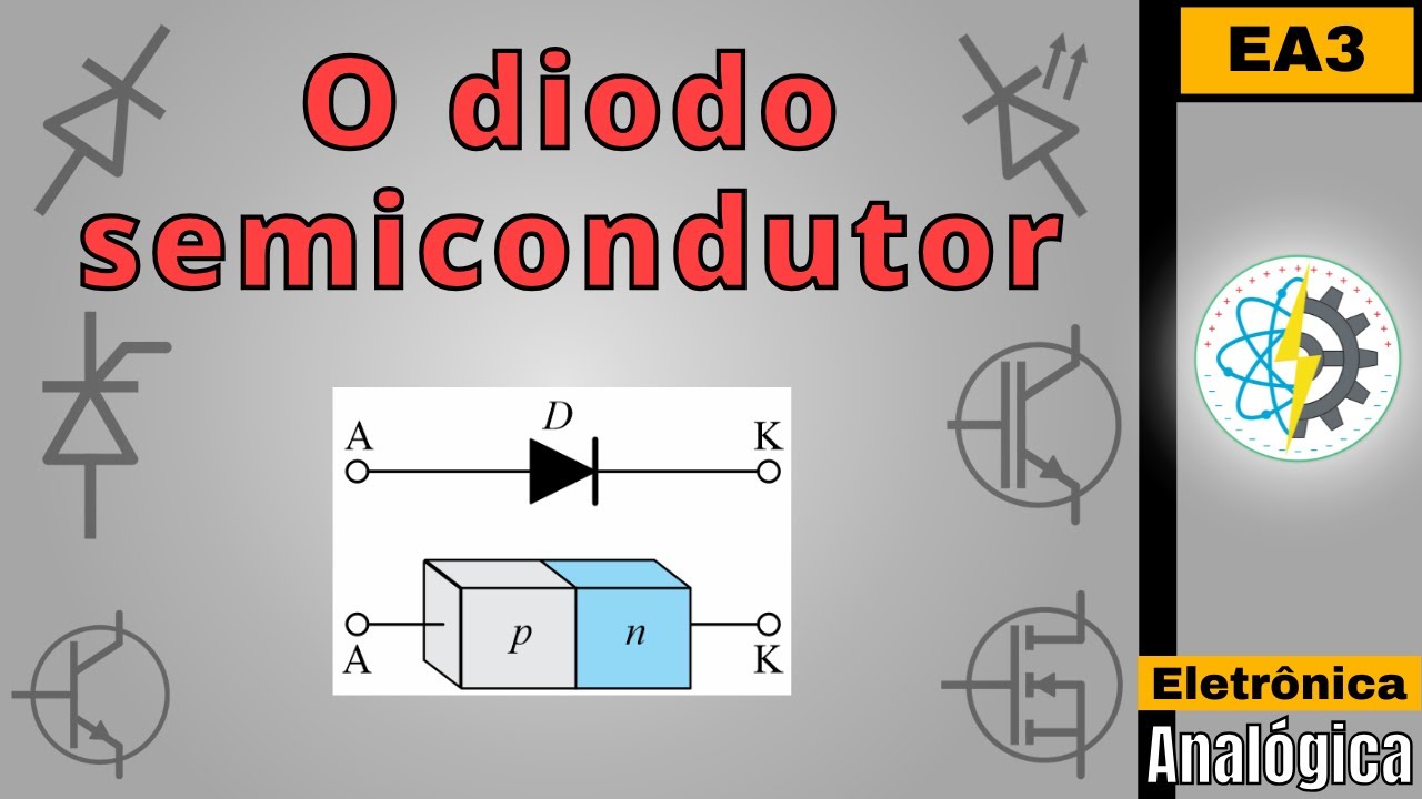









A PN junction is formed by joining P-type and N-type semiconductors, creating a boundary where electrons and holes diffuse across, generating an electric field that acts as a barrier; this barrier can be overcome by forward bias (reducing the barrier height to allow significant current flow) or prevented by reverse bias (increasing the barrier to block current), which enables the diode's fundamental property of conducting electricity in only one direction.
The PN Junction Explained: How Diodes Work | Semiconductor Physics
Added:Basic atomic structure and covalent bonding, specifically focusing on silicon and germanium atoms.
The concept of energy bands in solids, including the valence band, conduction band, and the bandgap.
The definition of intrinsic semiconductors and the concept of 'holes' as mobile positive charge carriers.
Fundamental electrostatics, including Coulomb's law, electric fields, and potential difference.
Biasing a PN junction: Analysis of forward bias and reverse bias conditions and their effect on the depletion width.
The Shockley diode equation and the non-linear current-voltage (I-V) characteristics of a real diode.
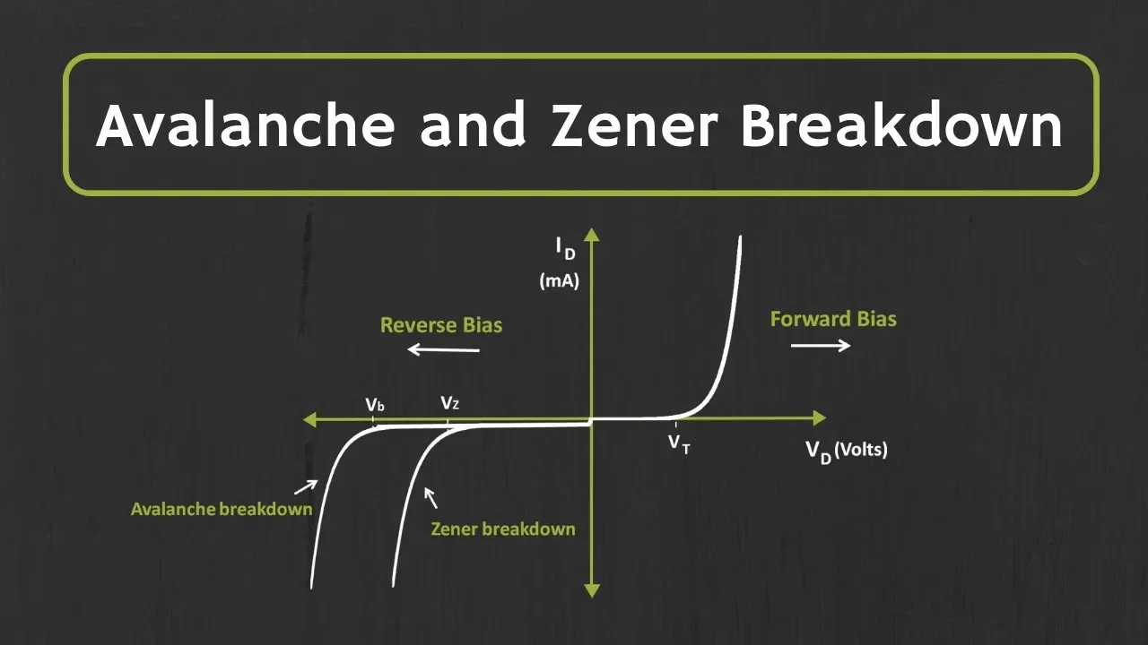
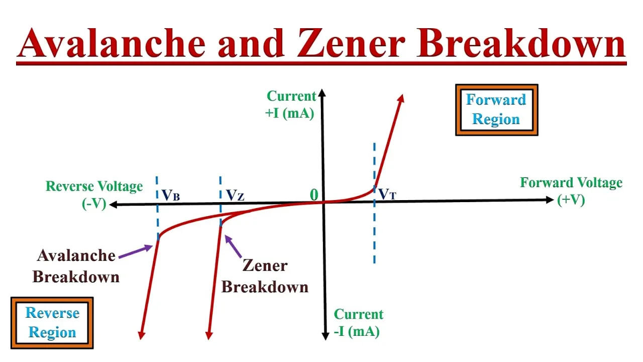
Diode breakdown mechanisms, specifically Zener breakdown and Avalanche breakdown.
Practical applications of diodes in electronic circuits, such as half-wave and full-wave rectifiers, clippers, and clampers.
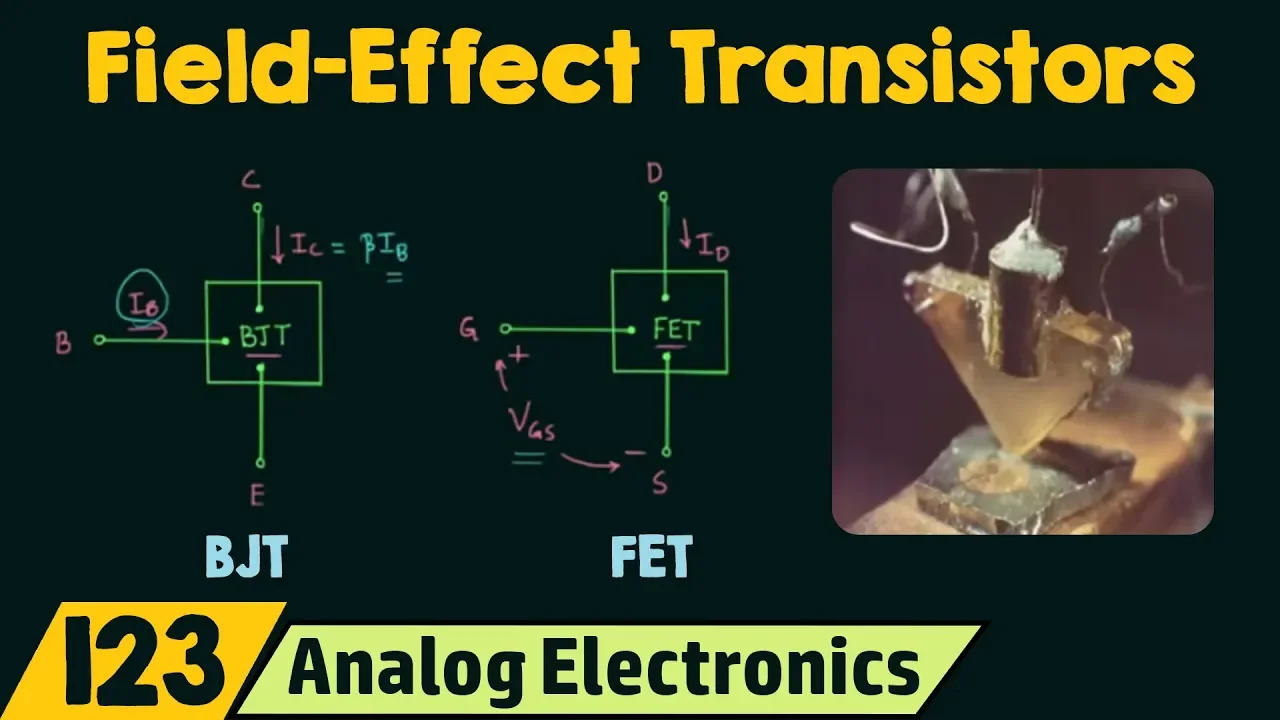
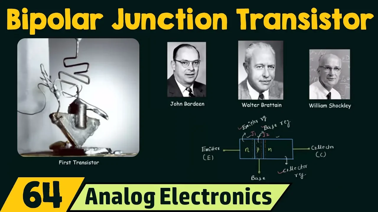
Introduction to multi-junction semiconductor devices, such as Bipolar Junction Transistors (BJTs) and Field-Effect Transistors (FETs).
1.2M views10.3Klikes10:36Original Release: 2013-05-04
[Music] we can find semiconductor PN Junctions in many places they form part of electronic and optoelectronic devices such as solar cells that transform solar energy into electrical energy light emitting diodes known as LEDs rectifier diodes and [Music] transistors to understand what semiconductor materials are and how PN Junctions are fabricated we need to dive into the atomic World currently the most well-known semiconductor is silicon in a silicon crystal each atom is bonded to its neighbors by four electrons forming calent bonds at low temperatures these electrons remain in the calent bonds when the temperature rises some of the electrons in the bonds are able to gain thermal energy and Escape they are now free to move and to conduct electricity at the same time the broken bonds can be occupied by electrons from other bonds for these electrons to move no additional energy is required on average this broken bond or new state is termed ho and behaves as a particle of positive charge and [Music] mass impurities can be introduced into the semiconductor substituting atoms of a different Atomic species for the Silicon atoms if the new atom has five electrons in its outer shell four of them will replace the four electron bonds of silicon the extra electron will be Loosely bound to the impurity at room temperature this fifth electron is liberated from its original atom becoming a conduction electron consequently the impurity acquires a positive charge this may result in the number of electrons in the doped material exceeding the number present in a pure semiconductor the number of implanted impurities can be controlled using the fabrication technology a semiconductor contain aing these impurities is called an N semiconductor since it has negative charge carriers the impurities are named donor impurities since they donate electrons an impurity with only three electrons in its outer shell can also be used the three outer electrons complete three of the four bonds the fourth Bond remains unoccupied however at room temperature the electrons from other bonds can move in to occupy this free space creating a hole in the material and negatively charged impurity as in the previous case the number of implanted impurities can be controlled using the fabrication technology so the number of holes in this dope material can be much greater than the number of holes in a pure semiconductor a semiconductor of this type is called a p semiconductor because it has positive charge carriers and these impurities are named acceptor impurities since they accept an electron a PN Junction is a structure formed by neighboring regions with different dopings ptype and N type semiconductors the PN Junction is a crucial part of many devices such as for example the diode if a positive voltage drop is applied between the P terminal and the N terminal of a diode a large current can be observed experimentally if we change the connectors and a positive voltage drop is applied between the N terminal and the P terminal an extremely small current negligible for most practical applications is observed experimentally the PN Junction shows this asymmetric Behavior the current can flow in One Direction but not in the other this is a peculiar Behavior which enables a wide spectrum of applications in circuits to understand this particular feature of the PN Junction we must consider two mechanisms that create an electric current the diffusion mechanism and the drift mechanism one way to understand the diffusion mechanism is to imagine two sets of different colored particles concentrated in two distinct zones if the particles are free to move in different directions their random motion tends to equalize their concentration in the whole volume diffusion is the physical mechanism which gives rise to free particles trying to occupy the maximum possible volume the drift mechanism is a movement caused by an electric field this electric field makes the positive charge carriers move in One Direction and the negative charge carriers in the other if there is an electric field in a region of space there will be an electric potential associated with it the electric field points in the direction in which the electric potential decreases the varying electric potential acts as a barrier preventing the charge movement its effects can be understood with the following analys ology let us consider a body moving at a certain speed in the gravitational field if the body Rises it loses kinetic energy and gains potential energy if the initial kinetic energy is not sufficient the body will be unable to cross the barrier but in the event that the initial kinetic energy is enough the body may be able to surmount it and even have sufficient kinetic energy left to enable it to continue its movement similarly the electric potential behaves like a barrier to the charged particles it allows the particles to amounted whenever the kinetic energy is great enough the process of fabricating a p injunction begins with an N type or ptype doped semiconductor into which the opposite type of impurity is introduced to understand how this structure works and what physical processes take place in it a dactic model is used the model consists of a p semiconductor perfectly matched to an N semiconductor the P semiconductor has a much higher hole concentration than the N semiconductor therefore holes from the P region will diffuse into the N region similarly electrons from the N region will diffuse into the P region the diffusion of electrons and holes creates a region depleted of free charg particles leaving behind the ionized impurities from which these charged particles come thus a region of positive ionized impurities and a region of negative ionized impurities appear in the PN Junction this special distribution of charges creates an electric field the electric potential associated with these fields acts as a barrier that prevents the displacement of the electrons and holes equilibrium is reached when the diffusion current equals the drift current the potential barrier is an obstacle for the diffusion current in the device it is possible able to reduce the height of this potential barrier by the application of an external voltage this increases the electric current by applying an external voltage from a battery the height of the potential barrier in the junction is modified if a positive voltage drop is applied between the p and N regions the barrier height is reduced A reduced barrier cannot prevent electrons and holes from diffusing across the structure an electric current appears in the junction due to the diffusion mechanism under these conditions the p and Junction is said to operate under a forward bias if the voltage is reversed and becomes greater in the N than the P region the barrier height increases preventing the electron and hold diffusion the electric current is then [Music] negligible in conclusion the PN Junction can only conduct in a single Direction giving rise to a current which increases very rapidly when the potential barrier is significant [Music] lowered besides being present in countless circuits and electronic components PN Junctions can also be found in opto electronic applications in devices such as LEDs photo diodes and solar cells the origin of the light emitted from an LED can be found in the physical phenomenon of recombination recombination is a process where an electron and a hole are annihilated releasing energy in the case of certain materials and under forward bias this energy is emitted as light the more electron ho pairs recombine the more intense this light is the operation of the photo diodes and solar cells is based on the opposite physical phenomenon generation thus a photon can create an electron hole pair which by its movement can generate an electric current to summarize PN Junctions so ubiquitous scenario environment close and distant it seems unbelievable that such a simple device is so useful and affect so much in our lives [Music] [Music] I see h [Music]
Up Next

4:18
Drift and Diffusion Currents in Semiconductors Explained
@arkafoundationclasses
112 views•2022-12-26

12:53
21cm Hyperfine Transition in Neutral Hydrogen: Radio Astronomy Basics
@AaronRobertParsons
12.4K views•2011-10-13

32:32
NMR Spin Physics I: Zeeman Effect, Resonance Condition & Larmor Frequency
@nptel-indianinstituteofsci8064
2.3K views•2024-01-17

27:14
Entropy and the Second Law of Thermodynamics Explained
@veritasium
27.5M views•2023-07-01
Related Study Plans & Knowledge Roadmaps
Structured learning paths in Physics
physics
Nuclear Physics (Decay, Fission & Reactors)
01Atomic Structure and the Binding Force
02Radioactive Decay and Half-Life
03Nuclear Fission Mechanics and Chain Reactions
+ 2 more learning modules
12h5 modules
Explore Roadmap
physics
Soft Matter (Polymers, Colloids & Rheology)
01Foundations of Soft Matter & Thermal Forces
02Polymer Physics and Macromolecules
03Colloids, Surfactants, and Self-Assembly
+ 2 more learning modules
38h5 modules
Explore Roadmap
physics
Analytical Mechanics: Lagrangian & Hamiltonian
01Mathematical Foundations: Calculus of Variations
02From Newtonian Mechanics to Constraint Dynamics
03The Principle of Least Action & Lagrangian Mechanics
+ 3 more learning modules
28h6 modules
Explore Roadmap
physics
General Relativity (Spacetime & Cosmology)
01Foundations of Relativity: Special Relativity
02The Geometry of Spacetime: Equivalence Principle & Curvature
03Einstein's Field Equations: The Mathematics of Gravity
+ 2 more learning modules
55h5 modules
Explore Roadmap