Semiconductor detectors are solid-state radiation detection devices that exploit the unique electronic properties of semiconductors, which have a narrow band gap (approximately 1 eV) allowing thermal promotion of electrons between the valence and conduction bands; when cooled to liquid nitrogen temperatures, the conduction band becomes empty, and incident radiation generates electron-hole pairs that are swept by an applied electric field to produce measurable electrical pulses, functioning similarly to ionization chambers but with charge carriers being electrons and holes rather than ions.
Semiconductor Detectors Explained: Energy Bands & Physics
Added:Deep Dive
Basic solid-state physics, specifically the concepts of energy bands, valence bands, conduction bands, and band gaps.
2.CONCEPT OF ENERGY BANDS | BASIC ELEX.| by Ranjan sir
895
This comprehensive section covers the fundamental concepts of energy bands in solid-state physics. The instructor explains that single atoms have discrete energy levels where electrons occupy specific orbits, but in solid crystalline structures containing approximately 10^23 atoms, atoms are tightly packed together causing interactions between neighboring atoms. This interaction causes discrete energy levels to split and form continuous energy bands. The Pauli Exclusion Principle prevents electrons from occupying identical quantum states, leading to the splitting of sharp discrete levels into multiple closely spaced levels that appear continuous. The two most important bands for electrical conductivity are the valence band (containing bound electrons) and the conduction band (containing free electrons). The forbidden energy gap (FEG) is the separation between valence and conduction bands where electrons cannot reside. The FEG varies by material: conductors have overlapping bands with zero FEG, insulators have very large FEG (>5 eV), and semiconductors have intermediate FEG (~1 eV). The width of the FEG indicates the bonding strength of valence electrons with their nucleus - wider FEG means tighter bonding.
Click to watch →

Band theory of solids | for Semiconductors, Conductors & Insulators |
4.7K
In solid-state physics, the valence band consists of filled energy levels containing electrons, while the conduction band consists of empty or partially filled energy levels above the valence band. The band gap is the energy difference between the top of the valence band and the bottom of the conduction band. Electrons must gain sufficient energy to cross this gap to participate in conduction. Materials are classified based on the size of this band gap: conductors have no band gap (bands overlap), semiconductors have small gaps, and insulators have large gaps.
Click to watch →

Band Theory of Solid | Diploma 2nd semester physics | Applied physics Band Theory of Solid (part-1)
11.2K
An energy band is the range of energy levels electrons can occupy in a solid. Energy bands are separated by band gaps, which are forbidden energy ranges where no electron states exist. The valence band represents energy levels occupied by valence electrons (outermost electrons). The band gap is the energy difference between valence and conduction bands, determining material properties.
Click to watch →

Plus Two Physics Model Exam | 60 Sure Questions | Eduport Plus Two
113.1K
In solids, electrons occupy energy bands: (1) Valence band - filled with electrons, (2) Conduction band - where electrons can move freely, (3) Band gap - energy difference between valence and conduction bands. Conductors have overlapping bands, semiconductors have small band gaps (< 3 eV), and insulators have large band gaps (> 3 eV).
Click to watch →

Energy Bands in solid in Hindi | Valence band | Conduction Band | Forbidden Energy Gap | Tutor Abhi
1.9K
In solid materials, electrons occupy continuous energy ranges called energy bands, formed when discrete atomic energy levels broaden due to electron interactions between neighboring atoms. The valence band contains bound valence electrons that participate in chemical bonding, while the conduction band contains free electrons that conduct electricity. The band gap is the energy difference between these two bands, representing the minimum energy required for an electron to transition from the valence band to the conduction band. The size of the band gap determines a material's electrical properties: larger band gaps indicate stronger electron binding and more difficult electron liberation, while smaller band gaps facilitate easier electron movement and better conductivity.
Click to watch →
Deep Dive
The fundamentals of semiconductor materials, including n-type and p-type doping.

Solid States || Electrical Properties | n & p Semiconductors | Doping || JEE || NEET || BOARDS
34.3K
This section covers semiconductor doping in detail. N-type semiconductors are created by adding Group 15 elements (like phosphorus) to germanium. These dopants have 5 valence electrons while germanium has 4, creating an extra free electron that conducts electricity. P-type semiconductors are created by adding Group 13 elements (like boron) to germanium. These dopants have only 3 valence electrons, creating a 'hole' that can accept electrons from neighboring atoms. In n-type materials, free electrons are majority charge carriers (negative charge). In p-type materials, holes are majority charge carriers (positive charge). Current flows in the direction of hole movement, while electrons move in the opposite direction to fill holes.
Click to watch →

ECE Purdue Semiconductor Fundamentals L1.6: Materials Properties - Doping
15.5K
Semiconductor doping involves intentionally introducing impurity atoms from different periodic table columns into a crystalline lattice to control electrical conductivity; n-type doping (using column V elements like phosphorus or arsenic) adds extra electrons that become weakly bound (binding energy ~0.05 eV) and easily donated to the conduction band at room temperature, while p-type doping (using column III elements like boron or gallium) creates holes that can move through the lattice, with carrier concentrations following the relationship n ≈ ND+ for n-type and p ≈ NA- for p-type, and the temperature-dependent behavior showing freeze-out at low temperatures, extrinsic conduction at moderate temperatures, and intrinsic conduction at high temperatures where thermal excitation overwhelms doping effects.
Click to watch →

العناصر والدارات الإلكترونية ١ ، الهندسة المعلوماتية جامعة قرطبة الخاصة📚📍ℂℙ𝕌 .
1.2K
Semiconductor materials are classified into N-type and P-type based on their charge carriers. N-type semiconductors have electrons as majority carriers and holes as minority carriers, while P-type semiconductors have holes as majority carriers and electrons as minority carriers. The type of semiconductor is determined by the impurity atoms added: pentavalent impurities (such as phosphorus, arsenic, or antimony) create N-type semiconductors by adding extra electrons, while trivalent impurities (such as boron, aluminum, gallium, or indium) create P-type semiconductors by creating holes. This fundamental principle of doping is essential for understanding semiconductor behavior and electronic device operation.
Click to watch →

Electronic 1| Semiconductors 2
1.1K
Semiconductors are fundamental electronic materials. Doping transforms intrinsic semiconductors into extrinsic ones by adding impurities. N-type semiconductors are created by doping with Group 5 elements like phosphorus (5 valence electrons), which donate extra electrons making them majority carriers. P-type semiconductors are created by doping with Group 3 elements like boron (3 valence electrons), which create holes making them majority carriers. At thermal equilibrium, n × p = ni². In doped materials, majority carrier concentration equals dopant concentration, while minority carrier concentration is much lower.
Click to watch →

أقوى ملخص للفصل الثامن فى الفيزياء لطلاب 3 ثانوى حيلملك الدنيا | مع الكينج محمود فؤاد 📚
6.1K
N-type semiconductors are created by doping pure silicon with pentavalent impurities (Phosphorus, Arsenic, Antimony) that have 5 valence electrons. When a pentavalent atom replaces a silicon atom, it forms 4 covalent bonds but has one extra electron that becomes free. This extra electron is the majority charge carrier. The dopant atom becomes a positive ion (donor atom). P-type semiconductors are created by doping pure silicon with trivalent impurities (Boron, Aluminum, Gallium) that have 3 valence electrons. When a trivalent atom replaces a silicon atom, it can only form 3 covalent bonds, leaving one bond incomplete (a hole). A neighboring silicon atom provides an electron to fill this hole, creating a positive ion (acceptor atom) and a free hole. In N-type semiconductors, free electrons are the majority carriers and holes are the minority carriers. In P-type semiconductors, holes are the majority carriers and free electrons are the minority carriers. Both types remain electrically neutral overall.
Click to watch →
Deep Dive
The operating principles of a p-n junction, including the formation of a depletion region and the behavior under bias.
Semiconductor | Physics For CUET 2025 | CUET SAFAL 3.0🔥
192.7K
A P-N junction forms when P-type and N-type semiconductors are joined. Electrons diffuse from N to P while holes diffuse from P to N, creating a depletion layer depleted of mobile charge carriers. Fixed ions remain: positive in N-type and negative in P-type regions, creating an electric field opposing further diffusion. The barrier potential is 0.7V for silicon and 0.3V for germanium. Forward bias (positive to P, negative to N) reduces barrier potential and depletion width, allowing current flow. Reverse bias (positive to N, negative to P) increases barrier potential and depletion width, blocking majority carrier flow. Donors donate electrons, acceptors accept electrons, creating the fixed charges.
Click to watch →

Semiconductors, One shot video for Class 12 Physics NCERT for CBSE 2024 Subscribe @ArvindAcademy
109.8K
A P-N junction is formed by joining p-type and n-type semiconductors in a single crystal. The junction is the boundary between the p-type and n-type regions. When a P-N junction is formed, majority carriers diffuse across the junction: electrons from n-side diffuse to p-side, and holes from p-side diffuse to n-side. This diffusion creates a region depleted of free charge carriers called the depletion region. The depletion region contains only immobile ions: positive ions on the n-side and negative ions on the p-side. This region has no free charge carriers to conduct current. The immobile ions create an electric field called the built-in electric field, pointing from the n-side (positive ions) to the p-side (negative ions). The potential difference across the P-N junction is called the barrier potential (Vb), approximately 0.7 V for silicon and 0.3 V for germanium at equilibrium. This barrier potential prevents majority carriers from diffusing across the junction and is responsible for the rectifying behavior of P-N junctions.
Click to watch →

Introduction to PN Junction Diode | Semiconductor Devices & Digital Circuits | L9 | #AnkitGoyal
4.2K
The depletion region forms when electrons diffuse from N-type to P-type and holes diffuse from P-type to N-type. As electrons leave the N-type region, they leave behind positively charged donor ions. As holes leave the P-type region, they leave behind negatively charged acceptor ions. This creates a region with no free charge carriers, only fixed ions. Barrier potential (built-in potential) is the voltage that develops across the depletion region due to the electric field. It acts as a barrier that prevents charge carriers from crossing the junction under zero bias conditions. The P-type side has higher potential (positive ions) and the N-type side has lower potential (negative ions). A PN junction is formed by doping a single crystal of semiconductor material on one side with pentavalent impurities (P-type) and on the other side with trivalent impurities (N-type). Biasing refers to the external voltage applied to a PN junction. Forward bias connects the positive terminal to the P-type side and negative terminal to the N-type side. Reverse bias reverses these connections. The depletion region width changes with applied bias - it widens under reverse bias and narrows under forward bias.
Click to watch →

Semiconductor and Structure of Atom | Crash Course | IMP Questions | Kurukshetra Crash Course 🔥
1.5K
This section explains PN junction formation and operation. When p-type and n-type materials join, electrons diffuse to fill p-side holes and vice versa, creating an induced electric field with positive charges on the n-side and negative on the p-side. The depletion region forms where carriers are depleted, with a built-in potential of ~0.5 eV across ~10^-6 m width. Forward bias connects positive to p-side and negative to n-side, reducing the electric field, narrowing the depletion region, and allowing majority carrier diffusion current to dominate. Reverse bias connects positive to n-side and negative to p-side, increasing the electric field, widening the depletion region, and causing drift current to dominate, ideally resulting in zero net current.
Click to watch →

Master video for PN junction - PN junction, Biasing of PN junction #depletionlayer #biasing #juction
1.1K
PN junction is the fundamental building block of semiconductor devices, applicable to both diodes and transistors. A PN junction forms when P-type semiconductor (doped with trivalent impurities creating holes as majority carriers) is joined to N-type semiconductor (doped with pentavalent impurities creating electrons as majority carriers). The boundary creates a PN junction diode with anode (P-side) and cathode (N-side). The depletion region forms due to diffusion of majority carriers - holes from P-region diffuse into N-region and recombine with electrons, while electrons from N-region diffuse into P-region and recombine with holes. This creates a region depleted of mobile charge carriers containing only fixed ions: negative acceptor ions in P-region and positive donor ions in N-region. These uncovered charges create an electric field that opposes further diffusion, establishing a barrier potential. The barrier potential prevents majority carriers from crossing the junction, acting as a one-way valve. The depletion region width depends on doping levels - higher doping results in thinner depletion region. Forward biasing connects battery positive to P-type and negative to N-type, reducing the barrier potential and narrowing the depletion region. This allows majority carriers to diffuse across the junction, creating large current flow. For silicon diodes, threshold voltage is 0.7V; for germanium, it's 0.3V. Below threshold, minimal current flows; above threshold, current increases exponentially.
Click to watch →
Deep Dive
Basic concepts of ionizing radiation (such as alpha particles, beta particles, and gamma rays) and how they interact with matter.

Interaction of radiations with matter | in Urdu/Hindi | class 12 physics | physics ka safar
19.6K
This lecture introduces the interaction of radiation with matter, focusing on alpha, beta, and gamma radiation. Using an analogy of three people with different body sizes (thick, medium, thin), the instructor explains that alpha particles are the heaviest and most ionizing but least penetrating, beta particles are lighter with moderate properties, and gamma rays are the lightest with the highest penetration power. Alpha particles are helium nuclei with +2 charge, beta particles are high-speed electrons with -1 charge, and gamma rays are photons with no charge or mass. The instructor emphasizes that understanding these fundamental properties is essential for studying radiation behavior.
Click to watch →

Short Questions of Chapter 21 || Nuclear Physics || 12th Class Physics
31K
Alpha particles are helium nuclei (2 protons, 2 neutrons) with +2 charge, highly ionizing but with low penetrating power, stopped by paper or skin. Beta particles are high-energy electrons with -1 charge, moderately penetrating, and can eject electrons from atoms through electrostatic repulsion. Gamma rays are electromagnetic radiation with no mass or charge, having high penetrating power. The interaction of electromagnetic radiation with matter depends on energy: low-energy causes photoelectric effect, medium-energy causes Compton scattering, and high-energy causes pair production. These interactions determine how radiation deposits energy in matter.
Click to watch →

FMPM MOOCs - Interactions des rayonnements ionisants avec la matière - Pr. Bsiss
28.3K
Ionizing radiation interacts with matter through two main mechanisms: charged particles (electrons, alpha particles, protons) cause direct ionization via collisions with electrons and nuclei, losing energy progressively and creating the Bragg peak for heavy particles, while photons (X-rays and gamma rays) interact through three processes—photoelectric effect (complete absorption by inner-shell electrons), Compton scattering (partial energy transfer to outer-shell electrons), and pair production (photon conversion to electron-positron pair when energy exceeds 1.022 MeV)—with attenuation following an exponential law I = I₀e^(-μx).
Click to watch →
La biophysique des rayonnements ionisants - 1er année médecine - P01
621
Ionizing radiation is energy transfer from a source that can remove electrons from atoms, creating ions; it includes three main types—alpha particles (helium nuclei, +2 charge, high ionizing power, low penetration), beta particles (electrons/positrons, -1/+1 charge, moderate ionizing power, moderate penetration), and gamma rays (electromagnetic waves, no charge, low ionizing power, high penetration)—with an inverse relationship between ionizing power and penetrating power, and three interaction outcomes with matter: partial energy absorption, complete energy absorption, or no interaction (pass-through).
Click to watch →

All of PARTICLES & QUANTUM in 10 minutes - A-level Physics Revision Mindmap
104.3K
Ionizing radiation includes alpha, beta, and gamma rays, all capable of giving electrons enough energy to escape atoms or molecules. An alpha particle is a helium nucleus (2 protons, 2 neutrons) - highly ionizing but weakly penetrating, stopped by paper or a few centimeters of air. A beta particle is a fast-moving electron with medium ionizing and penetrating ability, stopped by a few millimeters of aluminum. Gamma radiation consists of high-energy photons emitted from energetic nuclei - weakly ionizing but highly penetrative, requiring concrete or lead to significantly reduce intensity.
Click to watch →
Prerequisite Knowledge
- Concept 01Basic solid-state physics, specifically the concepts of energy bands, valence bands, conduction bands, and band gaps.
- Concept 02The fundamentals of semiconductor materials, including n-type and p-type doping.
- Concept 03The operating principles of a p-n junction, including the formation of a depletion region and the behavior under bias.
- Concept 04Basic concepts of ionizing radiation (such as alpha particles, beta particles, and gamma rays) and how they interact with matter.
Subsequent Learning
- Step 01Specific high-performance semiconductor detectors, such as High-Purity Germanium (HPGe) and Silicon Drift Detectors (SDDs).
- Step 02Readout electronics and signal processing, including preamplifiers and pulse-shaping networks used to analyze detector outputs.
- Step 03Gamma-ray spectroscopy and energy resolution analysis, including the interpretation of energy spectra.
- Step 04The impact of radiation damage on semiconductor lattices and techniques for noise mitigation, such as cryogenic cooling.
Semiconductor Basics
Detector Operation
Semiconductor Basics
0:00Playing Section
- 1
Explains energy bands in solid-state physics, including valence and conduction bands.
- 2
Distinguishes insulators, conductors, and semiconductors based on band gap energies.
- 3
Highlights that semiconductors have a narrow gap allowing thermal electron promotion.
Scintillation and Gaseous Detection: The Case for Non-Semiconductor Radiation Sensors
While semiconductor detectors excel in energy resolution due to their narrow band gaps, they are often impractical for large-scale, cost-effective, or highly rugged applications. Alternative detection technologies, such as scintillation detectors (which convert ionizing radiation into light) and gaseous ionization detectors (like Geiger-Müller counters), offer significant advantages. Scintillators can be manufactured in much larger volumes at a fraction of the cost, making them superior for high-energy gamma-ray detection where stopping power is crucial. Furthermore, gaseous detectors are highly durable and do not suffer from the permanent lattice radiation damage (Frenkel defects) that degrades semiconductor performance over time, nor do they require the complex cryogenic cooling systems often needed for high-purity semiconductor sensors.
Deep Dive
Specific high-performance semiconductor detectors, such as High-Purity Germanium (HPGe) and Silicon Drift Detectors (SDDs).

Pittcon 2012 - Waters Symposium - Abstract 4
324
Silicon drift detectors (SDDs) replaced large collecting electrodes with tiny central anodes guided by radial electric fields, enabling larger active areas without increased noise. Third-generation SDDs achieved 25 mm² area with 125 eV resolution and 8,500:1 peak-to-background ratio, stable to 3 million counts/second. Advanced preamplifiers optimized for 1 μs peaking times improved resolution to 130 eV. Silicon nitride windows enabled carbon detection below silicon's K-edge. Current state-of-the-art includes PIN diodes (50-150 eV, 100,000 cps) and SDDs (125 eV, over 1 million cps), with tens of thousands deployed in handheld XRF systems.
Click to watch →

Ю.А. Шитов и А.В. Лубашевский / Yu.A. Shitov and A.V. Lubashevsky
126
The vGEN experiment uses HPGe detectors with cryogenic cooling (liquid nitrogen or electronic) to achieve excellent energy resolution. The first-generation detectors achieved 78 eV resolution at 260 keV, essential for detecting small CEvNS recoil energies. Calibration uses pulse generators that inject signals identical to real events. The second-generation detectors showed worse performance (100+ eV) due to improper handling during transportation. Three of four detectors were sent for repair. The remaining detector achieved 250 eV threshold with ~70% efficiency. The energy resolution is limited by statistical fluctuations in charge collection and electronic noise.
Click to watch →

Semiconductor Detector for Charged Particle (DSE-2 UNIT-3(1) Lec-6)
499
High purity germanium detectors represent advanced semiconductor radiation detection technology. They offer superior performance including faster response times due to shorter pulse rise times, lower sensitivity to gamma background radiation, and excellent energy resolution for precise radiation energy measurements. The detectors achieve high energy resolution when the incident particle range is less than the junction thickness. These advantages make them essential tools in nuclear physics research and radiation monitoring applications.
Click to watch →

NST - Radioactivity, Nuclear Decay and Nuclear Models-6
522
Semiconductor detectors (HPGe, Si(Li)) use pure materials with small band gaps (0.69-1.11 eV). Doping creates n-type (extra electrons) or p-type (holes) materials; junctions form intrinsic zones for detection. Cooling (liquid nitrogen) minimizes thermal excitations. Reverse bias creates large intrinsic zones. HPGe offers excellent resolution (~1.85 keV at 662 keV) but lower efficiency than NaI(Tl); NaI(Tl) provides better efficiency but poorer resolution (~56 keV). Alpha spectroscopy requires thin detectors due to short alpha range. Surface barrier detectors show asymmetric peaks due to energy loss mechanisms. Gamma spectrometry enables multi-element analysis by simultaneously measuring multiple gamma lines from radioactive samples. Resolution is specified as FWHM at particular energies, enabling identification of closely spaced gamma lines when resolution exceeds line separation.
Click to watch →

Semiconductor Detector for Nuclear Radiation Detection
301
High-purity germanium detectors achieve depletion widths exceeding 2-3mm by reducing impurity levels to one dopant atom per 10^12 germanium atoms, eliminating the need for lithium drifting. Despite extreme purity, they maintain n-type or p-type classification and operate with reverse bias. Cooling remains necessary due to germanium's narrow bandgap generating thermally excited carriers at room temperature. These detectors provide superior energy resolution compared to lithium-drifted alternatives, achieving much narrower FWHM peaks. Key advantages include room-temperature storage capability, faster production timelines, and elimination of continuous cooling requirements during non-operation. Compound semiconductors like CdTe and HgI2 eliminate cooling requirements but sacrifice energy resolution. Semiconductor detectors offer 100-1000x higher density than gas detectors, superior gamma spectroscopy resolution, compact size, and excellent time characteristics, though they require cryogenic cooling systems and suffer from radiation-induced degradation creating trapping centers that reduce efficiency.
Click to watch →
Deep Dive
Readout electronics and signal processing, including preamplifiers and pulse-shaping networks used to analyze detector outputs.

電子回路
264
A scintillation detector electronic system consists of four main components: high voltage power supply, preamplifier, amplifier, and multichannel analyzer. The high voltage power supply requires extreme stability (0.001% voltage adjustment, 0.005% per °C temperature stability) and must supply milliampere currents. The preamplifier converts current pulses to voltage pulses using capacitor, resistor, and op-amp circuits. The amplifier shapes pulses for ADC conversion while filtering noise. The multichannel analyzer classifies pulses by size, counts them, and displays a gamma ray spectrum where the horizontal axis represents energy and vertical axis represents count values. This spectrum enables determination of radioactive material type and intensity.
Click to watch →
![Signal Processing & Measured Energy Spectrum in a Scintillation Detector [L21]](https://i.ytimg.com/vi_webp/fOAS8GJNKPY/maxresdefault.webp)
Signal Processing & Measured Energy Spectrum in a Scintillation Detector [L21]
7.5K
This section covers the complete signal processing chain from detector output to usable data. Preamplifiers amplify weak signals, match impedances, and perform initial pulse shaping. Main amplifiers further amplify signals and reshape pulses to reduce dead time and pulse pileup. Key challenges include maintaining energy proportionality, dealing with baseline shifts, and accurately timing signal arrivals. The trade-off between pulse width (for faster processing) and signal-to-noise ratio is fundamental to detector design. Zero-crossover timing methods solve the leading edge problem by identifying true arrival times independent of signal amplitude.
Click to watch →

Gamma ray scintillation. 001 equip tour mov
589
The signal processing chain begins with the detector producing extremely small currents too weak for direct use. Two cables connect to the detector: one carries high voltage to the dynodes for electron amplification, while the other carries the resulting signal. The pre-amplifier (preamp) is essential because the raw detector signal is too small to process directly—it must first pass through the preamp, which boosts the signal without degrading its character. The preamp has its own power supply and includes an input capacitor filter. The amplified signal then goes to the main amplifier, which provides fine and coarse gain control (factors of 20, 50, 100), pulse shaping, and output configuration options (bipolar/unipolar).
Click to watch →

Ionscan 400B Airport substances detector
52.8K
The ion detector includes a preamplifier circuit with a 10 gigohm resistor at the collector end of the tube. Guard traces surround the detection area to minimize unwanted currents. The preamp detects the very small current of ions hitting the detector electrode. The output signal is processed through additional amplification stages before being analyzed by the system's electronics.
Click to watch →

А.Селюнин "Система считывания света в жидком..."/ A.Selyunin “The light readout system in liquid...”
120
The light readout electronics chain includes: silicon photomultipliers converting light to electrical signals, preamplifiers on PCB boards, variable gain amplifiers (24 channels, 0-26 dB adjustable), and 64-channel ADCs with 16-bit resolution and 16 MHz sampling. Synchronization uses White Rabbit technology for 8 ns accuracy. High voltage power provides 200 V at 500 mA per channel for 128 channels. The system uses industry-standard protocols for reliability. Calibration uses LEDs mounted on the detector back panel to measure time delays and characterize response.
Click to watch →
Deep Dive
Gamma-ray spectroscopy and energy resolution analysis, including the interpretation of energy spectra.
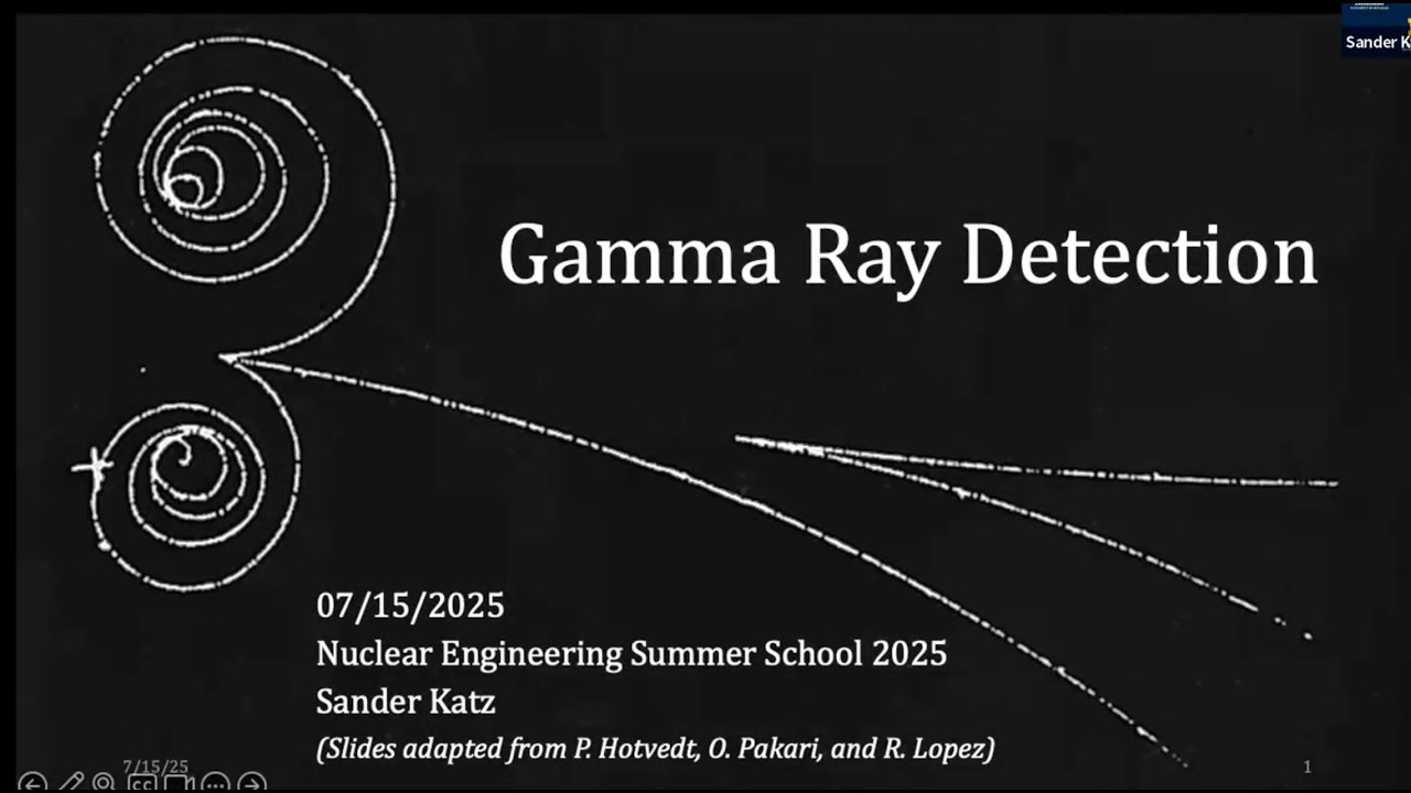
Gamma Detection -Sander Katz, NESS 2025
236
Gamma spectroscopy produces characteristic energy spectra with photoelectric peaks and Compton continua, where peak width (full width at half maximum) characterizes energy resolution—the narrower the peak, the better the ability to distinguish closely spaced gamma energies. Scintillation detectors achieve 2-500 eV per photoelectron, gaseous detectors ~30 eV, and semiconductor detectors 3-10 eV, with higher efficiency yielding better resolution. Poor resolution causes peak overlap, obscuring source identification. Photoelectric peaks appear as Gaussian features corresponding to specific gamma energies, enabling identification of radioactive isotopes like cobalt-60 through its characteristic 1.1 and 1.3 MeV gamma lines.
Click to watch →
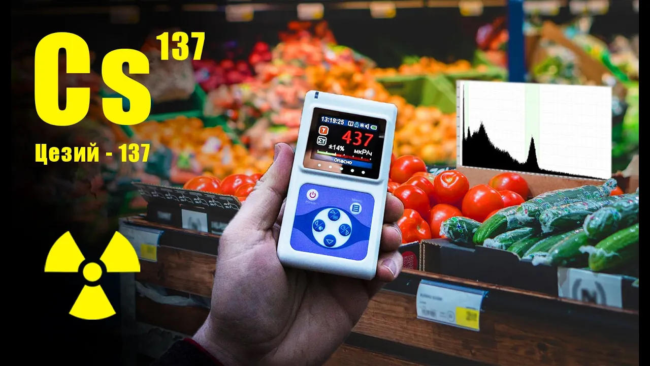
Радиоактивные продукты. Гамма-спектрометр
216.7K
Energy resolution is a key performance metric for gamma spectrometers, defined as the full width at half maximum (FWHM) of a photopeak divided by the peak energy. The video demonstrates measuring resolution using cesium-137 (662keV), showing approximately 8% resolution for a good NaI(Tl) crystal. Lower resolution (higher percentage) indicates poorer energy discrimination. The video notes that resolution can degrade over time as the crystal ages or degrades.
Click to watch →

Week 04: Lecture 19
1.8K
Scintillation detectors exhibit poor energy resolution (~6-7%) due to three limiting factors: low intrinsic light yield (~13% of gamma energy converted to photons), poor light collection efficiency (~20% of photons reaching PMT), and limited photocathode quantum efficiency (~20%). For a 1 MeV gamma ray, this produces approximately 1,300 photons, of which only ~130 reach the photocathode, generating ~26 photoelectrons. Energy resolution follows the formula FWHM = 2.35 × (100/√N)%, where N is photoelectron count. Gamma ray spectra display full energy peaks (photoelectric effect) sitting on Compton continuum backgrounds. Due to poor resolution, peaks appear broad and require linear background subtraction for accurate area integration. The resulting peak area divided by counting time yields counts per second, which can be corrected for detector efficiency and isotope abundance to determine absolute radioactivity.
Click to watch →

Laboratory demonstration of Gamma ray spectroscopy experiment (part 2)
7K
This extensive section explains gamma ray spectrum fundamentals and calibration methodology. Gamma spectra contain two primary features: the full energy peak (photopeak) where gamma rays deposit complete energy, and the Compton continuum from incomplete energy deposition. Energy resolution measures peak sharpness as full width at half maximum (FWHM), calculated by plotting counts versus voltage, performing linear interpolation, and subtracting background. Energy calibration converts voltage to energy using three calibration points from a single Cs-137 source: full energy peak at ~4.8V (662 keV), Compton edge at ~3.6V (300 keV), and backscatter peak at ~2.4V (150 keV). The backscatter peak forms when a lead plate increases backscattering events, providing the third essential calibration point for accurate energy conversion.
Click to watch →
34: Kervin Mathurin - Determining Energy Resolution from Inorganic Sources
155
This research demonstrates how gamma-ray photons interact with detector crystals through the photoelectric effect (where photons transfer all energy to electrons) and Compton scattering (where photons transfer partial energy depending on scattering angle), creating characteristic spectral features like the photopeak and Compton edge that enable identification of gamma-ray sources such as short gamma-ray bursts from neutron star collisions.
Click to watch →
Deep Dive
The impact of radiation damage on semiconductor lattices and techniques for noise mitigation, such as cryogenic cooling.
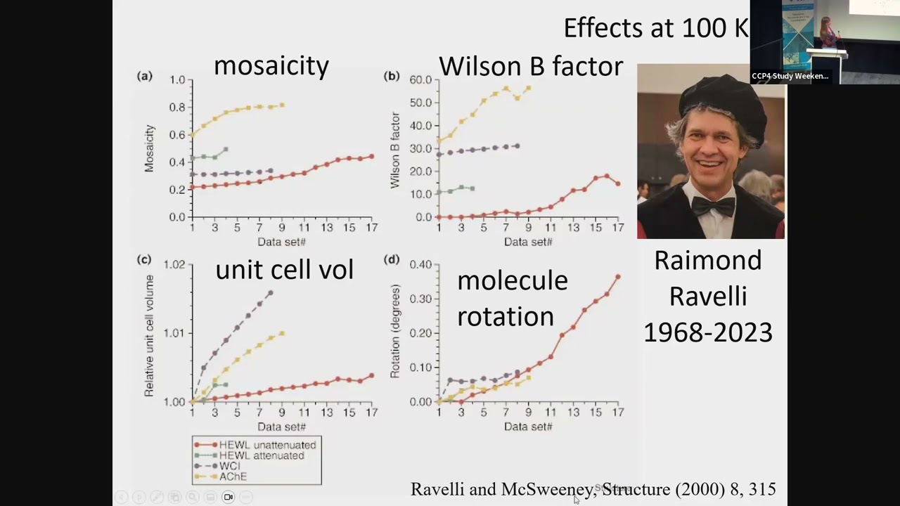
Identifying radiation damage and avoiding it in the first place - Elspeth Garman
174
At room temperature, radiation damage manifests as rapid loss of high-resolution reflections, with high 2-theta reflections disappearing first. The intensity decay follows an exponential pattern. Specific chemical damage includes disulfide bond breakage, reduction of metallo centers, and tyrosine modifications. At cryo-cooling (100 Kelvin), while damage occurs more slowly, it still affects the crystal: unit cell volume gradually increases due to gas collection at domain boundaries and dislocations, B-factors increase non-linearly, and high-resolution reflections decay faster than low-resolution ones. A concerning effect is molecular rotation within the unit cell, which compromises isomorphism for SAD experiments. Specific cryo-damage includes decarboxylation, cleavage of S-C bonds in methionine, and rupture of covalently-bound heavy atoms like bromine, iodine, and mercury.
Click to watch →

Professor Elspeth Garman delivers the 2010 Dorothy Hodgkin Memorial Lecture
1.9K
Dorothy Hodgkin discovered that mounting protein crystals in glass capillaries filled with liquid nitrogen gas prevents radiation damage during X-ray exposure. Without this technique, crystals exposed to air showed no useful diffraction spots. The capillary mounting keeps crystals hydrated while allowing X-rays to pass through. However, even cryogenic mounting at 100 Kelvin provides only about 70 times longer data collection time compared to room temperature. Studies show biological crystals can tolerate approximately 43 million gray of radiation before losing structural information. The main damage pathway involves radiolysis of water molecules producing reactive hydroxyl radicals that damage amino acid side chains, particularly disulfide bonds.
Click to watch →

News from the Lab | CMS - High-Granularity Calorimeter
686
Silicon detectors function as reverse-biased diodes that conduct only when particles pass through them, creating measurable signals. Radiation damage creates defects in the silicon crystal lattice that cause unwanted conduction (leakage current). This leakage current can overwhelm the actual particle signals. Cooling the silicon reduces this leakage current dramatically—approximately a factor of two reduction per 7°C decrease in temperature—allowing the detector to maintain useful operation despite accumulated radiation damage over years of operation.
Click to watch →
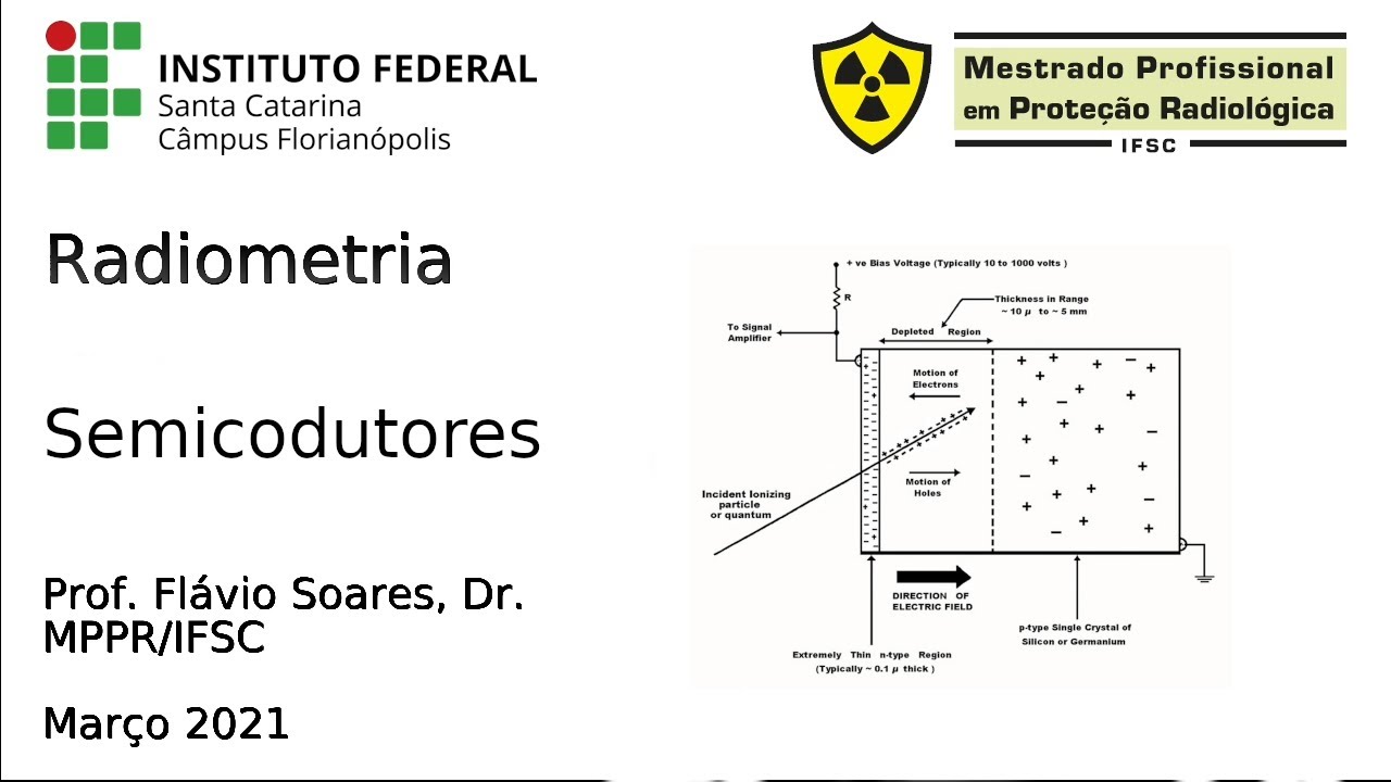
Aula 4. Dispositivos Ativos - Semicondutor
462
Cooling semiconductor detectors to cryogenic temperatures (around 170-180K) reduces electronic noise and increases the band gap. This allows stronger electric fields, faster carrier velocity, and reduced electron-hole recombination. Early semiconductor detectors required cooling, but modern detectors can operate at room temperature. However, electronic noise remains a challenge where electrons may randomly escape to the wrong side despite applied electric fields. Additionally, not all generated electron-hole pairs are collected efficiently. Despite these challenges, semiconductor detectors provide good energy resolution, capable of distinguishing between different radiation energies with high precision.
Click to watch →

Talk 1: Thermal Noise Limits in Radio Measurements
8.7K
Reducing the temperature of a circuit reduces its thermal noise power proportionally. Cooling from room temperature (290K) to liquid nitrogen temperature (29K, which is 1/10th of room temperature) reduces noise by 10 dB (since 10 log(1/10) = -10 dB). Further cooling to 2.9K reduces noise by another 10 dB. This is why radio astronomers and high-sensitivity receivers use cryogenic cooling to approach the theoretical kTB limit.
Click to watch →
Semiconductor Basics
Detector Operation
Semiconductor Basics
0:00- 1
Explains energy bands in solid-state physics, including valence and conduction bands.
- 2
Distinguishes insulators, conductors, and semiconductors based on band gap energies.
- 3
Highlights that semiconductors have a narrow gap allowing thermal electron promotion.
Scintillation and Gaseous Detection: The Case for Non-Semiconductor Radiation Sensors
While semiconductor detectors excel in energy resolution due to their narrow band gaps, they are often impractical for large-scale, cost-effective, or highly rugged applications. Alternative detection technologies, such as scintillation detectors (which convert ionizing radiation into light) and gaseous ionization detectors (like Geiger-Müller counters), offer significant advantages. Scintillators can be manufactured in much larger volumes at a fraction of the cost, making them superior for high-energy gamma-ray detection where stopping power is crucial. Furthermore, gaseous detectors are highly durable and do not suffer from the permanent lattice radiation damage (Frenkel defects) that degrades semiconductor performance over time, nor do they require the complex cryogenic cooling systems often needed for high-purity semiconductor sensors.
Basic solid-state physics, specifically the concepts of energy bands, valence bands, conduction bands, and band gaps.
The fundamentals of semiconductor materials, including n-type and p-type doping.
The operating principles of a p-n junction, including the formation of a depletion region and the behavior under bias.
Basic concepts of ionizing radiation (such as alpha particles, beta particles, and gamma rays) and how they interact with matter.
Specific high-performance semiconductor detectors, such as High-Purity Germanium (HPGe) and Silicon Drift Detectors (SDDs).
Readout electronics and signal processing, including preamplifiers and pulse-shaping networks used to analyze detector outputs.
Gamma-ray spectroscopy and energy resolution analysis, including the interpretation of energy spectra.
The impact of radiation damage on semiconductor lattices and techniques for noise mitigation, such as cryogenic cooling.
60.5K views390likes3:53@nuclearsecuritynsspiOriginal Release: 2010-12-02
now we're going to talk about semiconductors ration detectors this rather naturally leads to the question of exactly what's a semiconductor let's turn to the energy diagrams that are used in solid state physics and I can explain this rather easily these pictures are basically schematics of where the electrons stay in a material the bottom band is called the Veil Val band and the electrons in here are electrons that form bonds with neighboring atoms the conduction band represents a state within the material where the electrons can move freely from atom to atom at room temperature if the veilance band is separated from the conduction Band by more than about five electron volts thermal agitation caused by thermal energy IES cannot promote these electrons up to the conduction band these materials are insulators they neither conduct electricity nor heat very well examples are glass Ceramics wood you get the idea there are some materials uh almost all metals for example that the conduction band and the veilance span overlap as shown here this means that there are always free electrons that can move from atom to atom easily these materials are good conductors of electricity and good conductors of heat examples would be aluminum copper silver and gold there is also a strange group of actors that are called semiconductors in which the veilance band and the conduction bands are separated by about one electron volt thermal energies can kick electrons up and to this conduction band but it's rare and these promoted electrons fall back into the veence band fairly quickly other electrons are promoted and they fall back so the conduction band is being continuously filled and continuously emptied and so it's partially filled at best we can exploit this narrow band Gap to make a radiation detector if we cool the semiconducting material down to liquid nitrogen temperature the conduction band will be empty because thermal energies are now too low to kick the electrons into the conduction band and the conduction band quickly drains of electrons radiation interacting in the semiconductor can promote electrons into the conduction band an applied voltage will sweep these electrons and holes left by these missing electrons out of the detector thus semiconductor detectors are solid state devices that operate essentially like ionization Chambers the charge carriers in the semiconductors are not electrons and ions as in gas counters but electrons and holes radiation incident upon the semiconducting junction produces these electron hole pairs as it passes through it and these electrons and holes are Swept Away under the influence of an electric field and proper Electronics collect the charge and create a pulse as shown in a diagram here the P injunction is made as thin as possible by applying reverse bias voltage the depleted region that acts as the detector can be made Fairly large
Up Next

6:44
Cyclotron Principle, Construction & Working Explained | Class 12 Physics
@vnperceptions
1.5M views•2016-11-01

12:53
21cm Hyperfine Transition in Neutral Hydrogen: Radio Astronomy Basics
@AaronRobertParsons
12.4K views•2011-10-13
4:38
Radiation Detection: Gas Amplification and Ionization Chambers
@nuclearsecuritynsspi
12.5K views•2017-09-27

27:14
Entropy and the Second Law of Thermodynamics Explained
@veritasium
27.5M views•2023-07-01
Related Study Plans & Knowledge Roadmaps
Structured learning paths in Physics
physics
Nuclear Physics (Decay, Fission & Reactors)
01Atomic Structure and the Binding Force
02Radioactive Decay and Half-Life
03Nuclear Fission Mechanics and Chain Reactions
+ 2 more learning modules
12h5 modules
Explore Roadmap
physics
Soft Matter (Polymers, Colloids & Rheology)
01Foundations of Soft Matter & Thermal Forces
02Polymer Physics and Macromolecules
03Colloids, Surfactants, and Self-Assembly
+ 2 more learning modules
38h5 modules
Explore Roadmap
physics
Analytical Mechanics: Lagrangian & Hamiltonian
01Mathematical Foundations: Calculus of Variations
02From Newtonian Mechanics to Constraint Dynamics
03The Principle of Least Action & Lagrangian Mechanics
+ 3 more learning modules
28h6 modules
Explore Roadmap
physics
General Relativity (Spacetime & Cosmology)
01Foundations of Relativity: Special Relativity
02The Geometry of Spacetime: Equivalence Principle & Curvature
03Einstein's Field Equations: The Mathematics of Gravity
+ 2 more learning modules
55h5 modules
Explore Roadmap