





























As Moore's Law continues with vertical integration and stacked chiplets, the heat generated by densely packed transistors (now at 2nm/3nm scales) creates a fundamental cooling crisis, leading to 'dark silicon' where only portions of chips can operate simultaneously; emerging solutions include transistor-level microchannel cooling (achieving 1,700W/cm² heat flux) and TSMC's direct-on-chip water cooling (2.6kW dissipation), which bring coolant extremely close to heat sources to dramatically improve efficiency and enable future high-performance AI chips like Cerebras' wafer-scale engines that dissipate up to 25,000W.
Transistor-Level Cooling: Moore's Law's Future
Added:The definition and historical context of Moore's Law, including the physical and economic limitations of traditional semiconductor scaling.
Basic thermodynamics and heat transfer mechanisms, specifically thermal conduction, convection, and resistance in solid-state devices.
The fundamentals of semiconductor physics, including how transistor switching generates dynamic power dissipation, leakage currents, and waste heat.
Standard processor thermal management solutions, such as thermal interface materials (TIMs), integrated heat spreaders (IHS), and macro-scale liquid cooling blocks.
3D Integrated Circuits (3D ICs) and heterogeneous integration, exploring how vertical silicon stacking creates severe thermal bottlenecks that require on-die cooling solutions.
Microfluidic co-design, where electrical circuitry and fluidic cooling channels are designed concurrently on the same substrate using electronic design automation (EDA) tools.
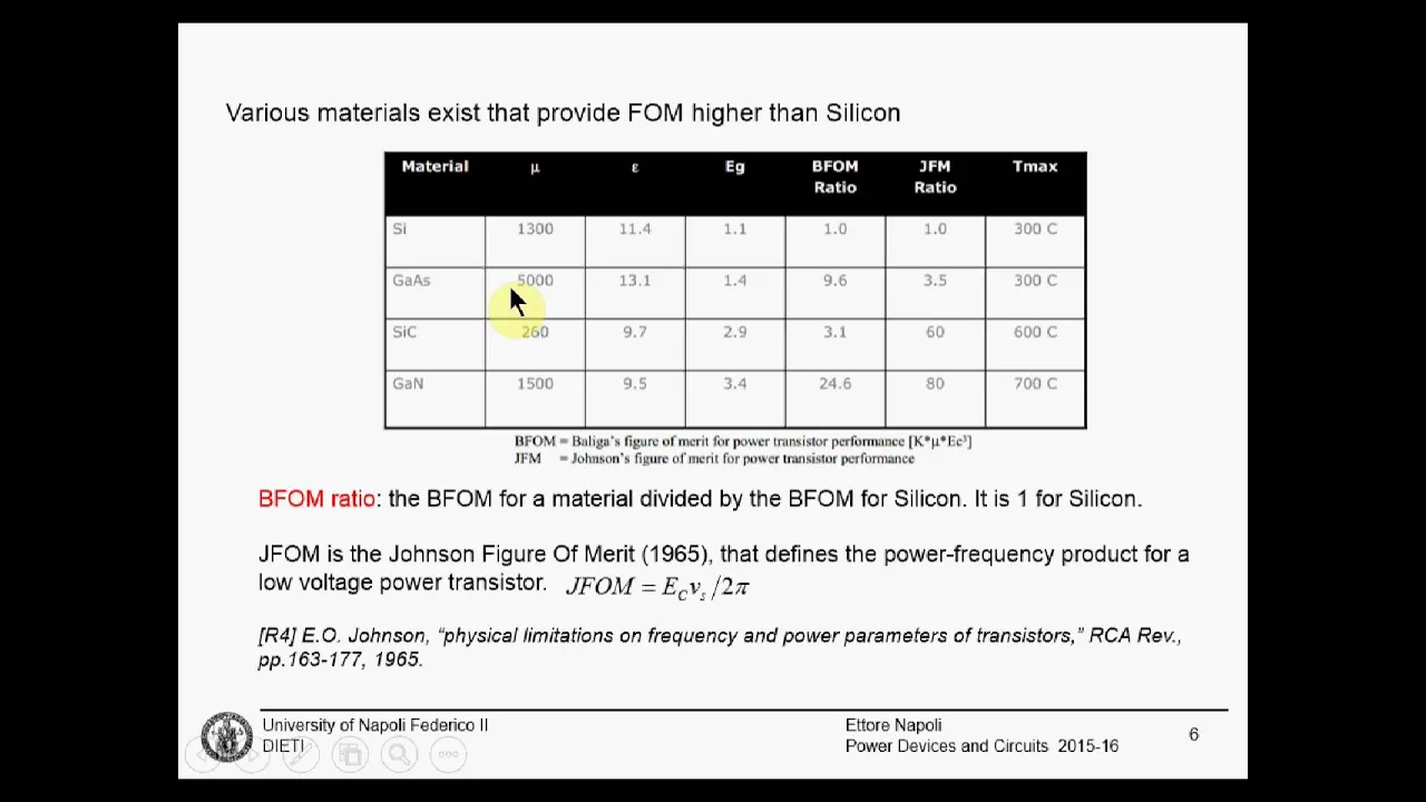
Advanced wide-bandgap semiconductor materials (such as Gallium Nitride and Silicon Carbide) and ultra-high thermal conductivity substrates like synthetic diamond.
Thermal-aware floorplanning and physical design algorithms used in chip layout to predict, distribute, and mitigate localized hotspots.
96.7K views7.6Klikes19:09Original Release: 2024-07-30
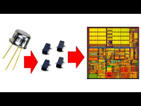
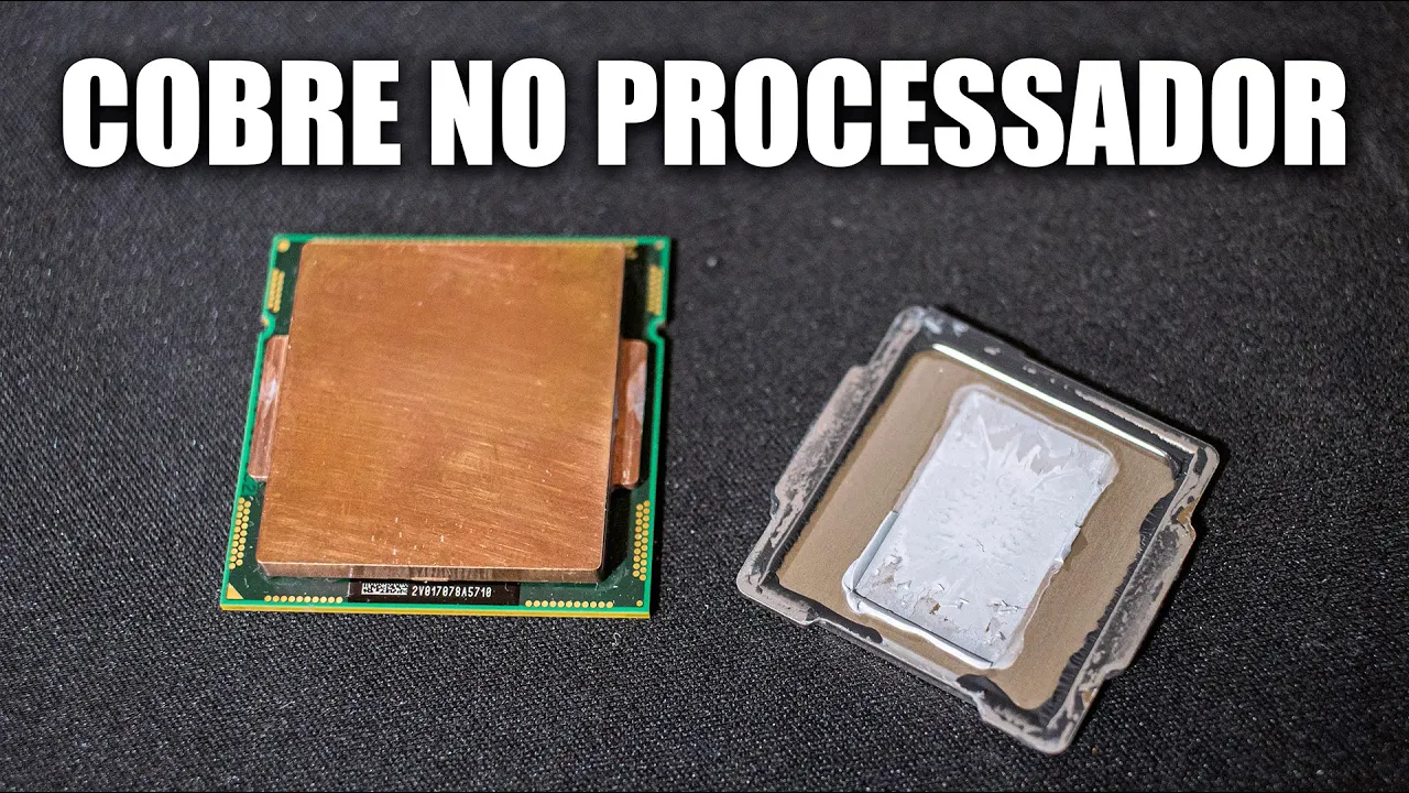
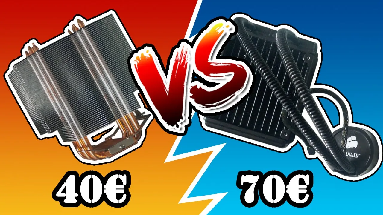
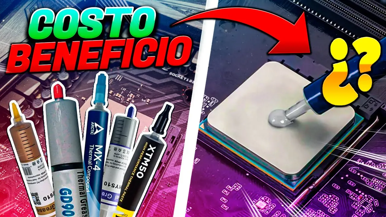
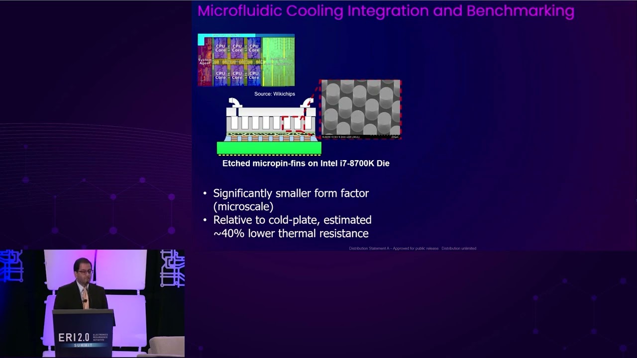
welcome back to Anastasi in Tech according to a new report by McKinsey computing demand will increase by a factor of at least 100 over the next 5 years and chip makers and semiconductor fabs are putting in a lot of effort to satisfy this demand for semiconductors this decade is all about vertical integration stacking chiplets on top of each other and stacking transistors and that's great for the performance but very problematic for cooling in this video I will explain how different cooling technologies are keeping Moore's law alive and the most interesting of all I will explain some brand new Transistor Level Cooling Technology that will save the chips of the future from roasting in their own heat this cooling technology is so cool that it has its own fan club current and future generation of chips have a fundamental problem by now we've managed to continuously improve the performance by packing more and more transistors into a size of a chocolate square right now the smallest transistors are just 2nm and 3nm allowing us to stuff massive 200 billion transistors into a tiny piece of silicon but now there is a problem because now there are so many transistors that they cannot be used all at once without the chip overheating and how much heat a chip dissipates measured in so-called TDP's which stands for Thermal Design Power and it's actually based on the maximum heat flux that we can remove from this chip if we take NVIDIA H100 GPU it's about 700W TDP and the latest NVIDIA Blackwell GPU dissipates about 1,000W of heat and one of the big problems here of such a chip that while this chip operates half of this area half of the silicon is actually dark silicon, dark silicon is a phenomenon where a significant portion of the transistors on the chip cannot be computing at the same time due to power and thermal constraints what makes it even worse is ongoing vertical integration because the future of the chips is in stacking them on top of each other it's all started by stacking chiplets small pieces of silicon that have their own function on top of each other back in 2022 AMD was the first to introduce V-cache technology when they stacked an additional cache memory on top of a CPU die and it's all acted as one single chip and the same trend is happening with chips building blocks transistors we are now at the pivotal moment in the history of transistors where we simply aren't able to achieve more with just FinFET architecture and now we are transitioning towards stacking nano sheets vertically and according to Imec by 2030 we will be stacking transistors on top of each other well what are we going to do with all this additional heat that is coming as a result of this just like the current heat wave in Europe heat is very disruptive what is heat - heat is a waste product of semiconductor usage when an electric field is applied to the transistor electric current flows in the channel from the source to the drain this results in conventional Joule heating due to the energy transfer from the electrons to the latencies while the chip performs operations transistors are switching from one to zero and back right and the power is being dissipated in the transistor devices as well as in interconnect wires and we have to get rid of this heat because heat is ruthless to the transistors and to the chip degrading its performance heat damages chips by accelerating the aging of components and decreasing their lifetime it also causes components side to firmly expand which causes signal distortion and dysfunction and the difficulty of removing the heat means that today's largest chips cannot use all their transistors at once so as not to overheat typically what we used to do is to conduct this heat out somewhere and then dissipate it there are many ways to keep chips cool by far the most popular solution involve cooling with air or liquid cooling with air works for some desktop chips and some of these server processors which dissipate about 280W however somewhere at around 300W TDP we reach the limit of what we can cool with air alone and above that we must switch to liquid cooling which can conduct up to 3,000 times more heat that air can this works for example with NVIDIA GPUs like A100 which can dissipate up to 1,000W of heat now air or liquid cooling is what we typically think of when we think of cooling but in reality things are much more interesting and much more complicated more advanced GPUs like AMD's MI300 or H100 employ a mixture of cooling strategies from my many years working in chip design I can tell you that the work on cooling starts already during the physical design phase here we have to keep in mind the switching activity of the blocks because some of the blocks will be switching more than the others some portions of the design might be more computationally intensive like a hardware accelerator and this will create a hot spot on the die and then we must place this block in a way that minimizes the peak temperature and also the gradient, temperature gradient across the chip and here EDA Tools (Electronic Design Automation Tools) and Power Analysis Tools are very helpful but that's usually not enough so for 3D chips we have to create heat corridors by placing TSVs in a particular way to help to spread the heat evenly so-called TSVs are through silicon vias which are copper connections that travel through silicon die these are used to connect chiplets in designs like AMD MI300 which has 13 chiplets stacked together and acting as one big chip and a similar technology is used in many other designs for example in Intel's Ponto Vecchio GPU TSVs are great because overall you're able to gain in performance and latency and of course you're also gaining in cooling because with TSVs we're providing both vertical and horizontal pathways for heat dissipation but again those are made of copper which is four times more conductive than silicon so they do help to guide some heat away but it's not a silver bullet unfortunately and unfortunately I happen to know that about 70% or even 75% of you watching this video are not subscribed to the channel so could you please do me a favor and consider subscribing to the channel this helps the channel more than you know because the bigger the channel gets the bigger the guests that I can interview for you get thank you eventually we end up guiding as much heat as we can to heat things or cold plates and some of the heat sinks have these bizarre fin shapes because the goal here is to maximize the area of the contact so when water is passing through these plates we can maximize the area of what we can actually cool and what's interesting some of the companies like Fabric8Labs using generative AI for designing these fins shapes in the most efficient way in any case everything has its limits so even heat sinks have their limits so if we want to cool down something very hot like DOJO training tile for example which dissipates about 15,000W of heat which is huge we clearly need something more sophisticated and more advanced here in the case of DOJO it's a whole new level because here the cooling is integrated in the package in one of my old deep dive videos on DOJO I discussed that they're use TSMC's integrated Fan Out Wafer Scale Packaging Technology in this case the cold plate is integrated right into the package and it's placed right on top of the computing tiles which generate all this massive amount of heat and then many tiny pipes so-called inlets and outlets are going through the package and then with water the heat is being moved away through these channels so this is an example of one of the recent TSMC inventions integrated into the package sophisticated power delivery and liquid cooling in case we need to take care of an extra hot chips now it's clear that we will see more powerful chips and more powerful AI ASICs (Application Specific Integrated Circuits) coming in the next years managing the extra heat is going to be one of the biggest problems for the electronics moving forward already now we have to go for immersion cooling and have sunk whole racks into tanks of liquid and the next step is clearly to bring this fluid even closer to the source of this heat just think for a moment how efficient could it be if coolant flew inside the processors this approach is called Embedded Cooling when they bring the liquid to the interior of the silicon super close to the computing cores that are actually running the job this is super efficient this idea goes back to the '90s when researchers from Stanford University suggested that heat could be removed more effectively if we add tiny micro-channels onto the chip itself this looked like a potential quick wind for cooling but back then this idea didn't get too much traction however with advancement of manufacturing process this solution has become more and more practical you know one of the problems which brought us to this point now that for a long time cooling and processing were developed separately and just a few years ago researchers at at my favourite École Polytechnique Fédérale de Lausanne brought this idea to the next level they designed the electronics and the cooling together from the very beginning they integrated cooling technology very close to the transistor themselves right near the channels where electrons flow basically they engineered these three-dimensional cooling channels within the chip itself right under the active part of the transistors this is a perfect spot it's just a few micrometers away from where the heat is actually produced and the idea is that it prevents heat from spreading throughout the device so a liquid coolant is pumped through these microchannels and eventually the cooling liquid flows inside an electronic chip a small comment here it's sounds really easy in theory but it's really hard to pull it off in practice without flooding the entire thing the liquid they used is deionized water the one that doesn't conduct electricity of course and with that they can handle huge amounts of heat up to 1,700W per square cm this is multiple times heat flux of today's GPUs according to the paper it improves the cooling efficiency at least by a factor of x50 and this will help to lighten up those dark parts of silicon we discussed before eventually boosting the performance and also we can reduce the amount of energy spent on cooling cool yes those GPUs NVIDIA GPUs that up to 500 to 600 TDP can do without this integrated cooling but the chips of the future like a wafer scale designs of the future will definitely benefit from this transistor level integrated cooling of course TSMC is also one of the front runners here they're working on a similar and quite interesting cooling technology they call it "Direct on cheap water cooling" basically they are creating micro channels directly on the silicon you see here these tiny trenches are edged directly into the silicon layer on top of the CPU they've tested several flavours of this cooling using different techniques shapes and liquids and they found that square pillar trenches perform the best and with that they able to dissipate up to 2.6 kilowatt of heat let me know your thoughts on this new technology in the comments great technology I believe we eventually will come to that that I'm pretty sure the biggest problem here that we will have to adjust the entire manufacturing process for that and this will drive up the costs and will make the chips of the future even more expensive and this technology will be able to cool down some of the hottest and most powerful chips of the future like one of the next versions of Cerebras wafer scale engine for example which dissipates up to 25,000W of heat if you don't know Cerebras it's a US based startup and they are building a large AI accelerator and they're actually one of the most successful AI chip startups to date who generate more cash than they burn you know their latest wafer scale engine three chips that they released this spring is a single gigantic chip of a size of 300mm wafer or a 12in wafer and this single chip is capable of 125 petaflops of AI compute by area it's 57 times larger than NVIDIA H100 so you can imagine how hot it can get in there when you have 900,000 AI cores on a single chip now try to guess how much heat this one generates and let me know in the comments actually it consumes somewhere from 15,000W up to 25,000W so it's very hot and Cerebras themselves said that cooling was one of the greatest challenges they had to solve and the solution is quite interesting the wafer floats on top of the heat sink plate and the heat sink has a labyrinth of micro-fin channels and then the water is pumped through this micro-fins to remove heat from the powered wafer although this chip is about 20 something cm and very thin its housing takes a lot of space and this space is mostly dedicated to cooling it takes about 1/3 of a standard track because it includes tubes pumps fans and a heat exchanger all of which takes a significant amount of space then when we talk of data centers full of NVIDIA GPUs here we typically use a mixture of air and liquid cooling combined with special data center layout and air flow management did you know that cooling of data centers takes about 40% of the total power this is huge and this goes to cooling the air and of course cooling the water and also a vast amount of water is being used for cooling like hundreds of billions of galloons yearly of course a much more efficient alternative is liquid immersion cooling and there are many different flavours to it but the idea is simple you sink your entire system into some liquid some non-conductive liquid like dielectric fluid so that liquid can contact every part of the system and as the system heats up the liquid will boil and evaporate this is a very efficient way of cooling compared to the classical one because it's like 50% more energy efficient and about 61% more area efficient I mean the area which is taken by the cooling system that's why all the Major servers vendors are now offering solution optimized for the immersion cooling however there is a big problem with the immersion cooling because at the moment we're using so-called PFAS chemicals which are super toxic they don't naturally break down they are contaminating environment and water and now the industry is moving away from them by 2025 we should stop the fabrication of the chemicals and we are researching alternative solutions which are more sustainable because we know, we see how efficient is immersion cooling and we need some alternative options here and of course AI models also can help us out here for example Google's Deep Mind built an AI model to optimize Google's data center cooling they took a lot of historical data collected by thousands of sensors like temperature power pump speeds and so on and they used this data to train a neural network to optimize for power usage effectiveness they've managed to find some patterns in the workloads and eventually used it to optimize efficiency and eventually managed to reduce their cooling system power consumption by 40% this is brilliant now to the outlook in my opinion on-die cooling what we discussed from EPFL and by TSMC these technologies are the cooling technologies of the future but TSMC's innovation pace is incredible and I'm pretty sure eventually they will be able to pull off something like this however there is also a tradeoff in that that this will also introduce additional challenges for the the power delivery if you don't know now we are transitioning to the backside power delivery I have a whole video about that I will link it below check it out later and this backside power delivery making this cooling challenge even more challenging let me know your thoughts in the comments and while we are talking about hot chips today the Hot Chip conference will take place at Stanford University between August 25th to 27th it's not sponsored I just want to bring your attention to this conference because it's one of the top conferences in the industry and you can attend both online and in person there will be discussions about AI in chip design all the recent advances in Hot Chips and of course about cooling technologies of the future if you would like to check out the speakers and register the link is in the description below and if you enjoyed this video I would really appreciate if you share this video with your friends colleagues or on social media and if you want to go beyond that you can support the channel by joining the patreon the link is in the description thank you so much for watching I will be back very soon with a new video ciao
Up Next

17:47
CAD Best Practices for Electronics Cooling Simulation
@SimscaleSimulation
1.8K views•2021-03-30

12:54
Triumph of Orthodoxy Icon: Byzantine Art & History Explained
@BenCallan
2.1K views•2024-08-06

9:49
FastAPI vs Flask vs Django: Choosing the Right Python Web Framework
@TechWithTim
302.5K views•2024-05-26

1:42
Game of Thrones Opening Credits: A Cinematic Analysis
@gameofthrones
46.3M views•2011-04-18
Related Study Plans & Knowledge Roadmaps
Structured learning paths in General & Interdisciplinary Studies
general-studies
Elevator Engineering: History, Physics & Cities
01From Hoists to Safety Brakes: The Dawn of Vertical Lift
02Hydraulic vs. Traction: The Engineering Physics of Elevators
03Modern Speed, Safety, and Algorithms
+ 2 more learning modules
12h5 modules
Explore Roadmap
general-studies
Rubber: Material Science, History & Geopolitics
01Origins of Natural Rubber & Mesoamerican History
02The Chemistry of Natural Rubber & Vulcanization
03The Geopolitics of the Rubber Boom & Colonization
+ 2 more learning modules
12h5 modules
Explore Roadmap
general-studies
Containerization: Evolution, Logistics & Trade
01Ancient Trade & Bulk Cargo: Amphorae to Barrels
02The Industrial Revolution & Cardboard Packaging
03The Containerization Revolution: Malcom McLean
+ 2 more learning modules
12h5 modules
Explore Roadmap
general-studies
Textile Tech: Evolution, Labor & Global Impact
01Pre-Industrial Textiles: Handloom & Cottage Industry
02Mechanization: The Spinning Jenny to the Power Loom
03The Factory System & Global Labor Transformation
+ 2 more learning modules
10h5 modules
Explore Roadmap