





![CFD - Computational Fluid Dynamics [Fluid Mechanics #17]](https://i.ytimg.com/vi/BdjPE9zxHCc/maxresdefault.jpg)











![[1] Electromagnetismo - Simulación multifísica en Ciencia e Ingeniería (5.5)](https://i.ytimg.com/vi/01ZGxg55l0A/maxresdefault.jpg)
![[Webinar] - Electromagnetic and multiphysics modeling of high-power busbars using SOLIDWORKS](https://i.ytimg.com/vi/sws_p7ww63U/hqdefault.jpg)
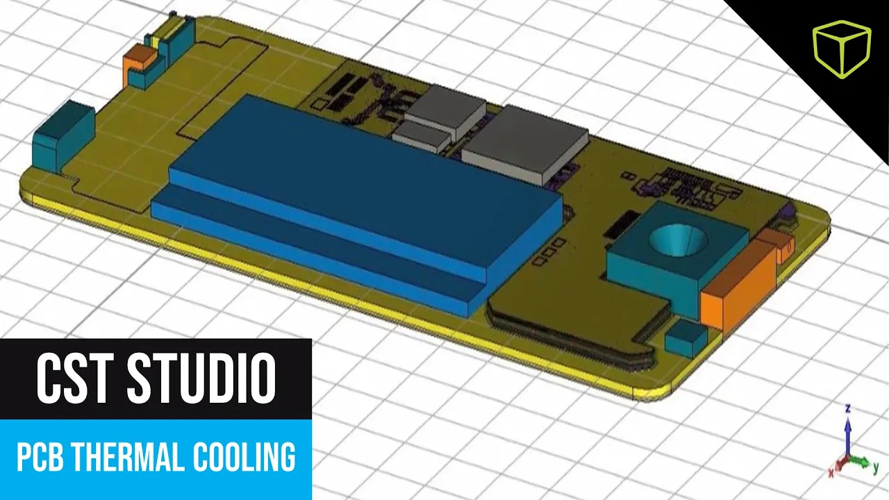
Successful CFD simulation requires proper CAD preparation by identifying and fixing common faults including intersections (overlapping entities), open volumes (unintended gaps or holes), and discontinuities (thin gaps between connected bodies), then simplifying the model by removing non-essential details like engravings, fillets, and screws to reduce mesh complexity while maintaining simulation accuracy.
CAD Best Practices for Electronics Cooling Simulation
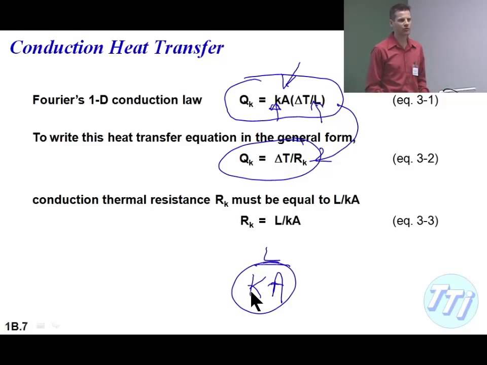
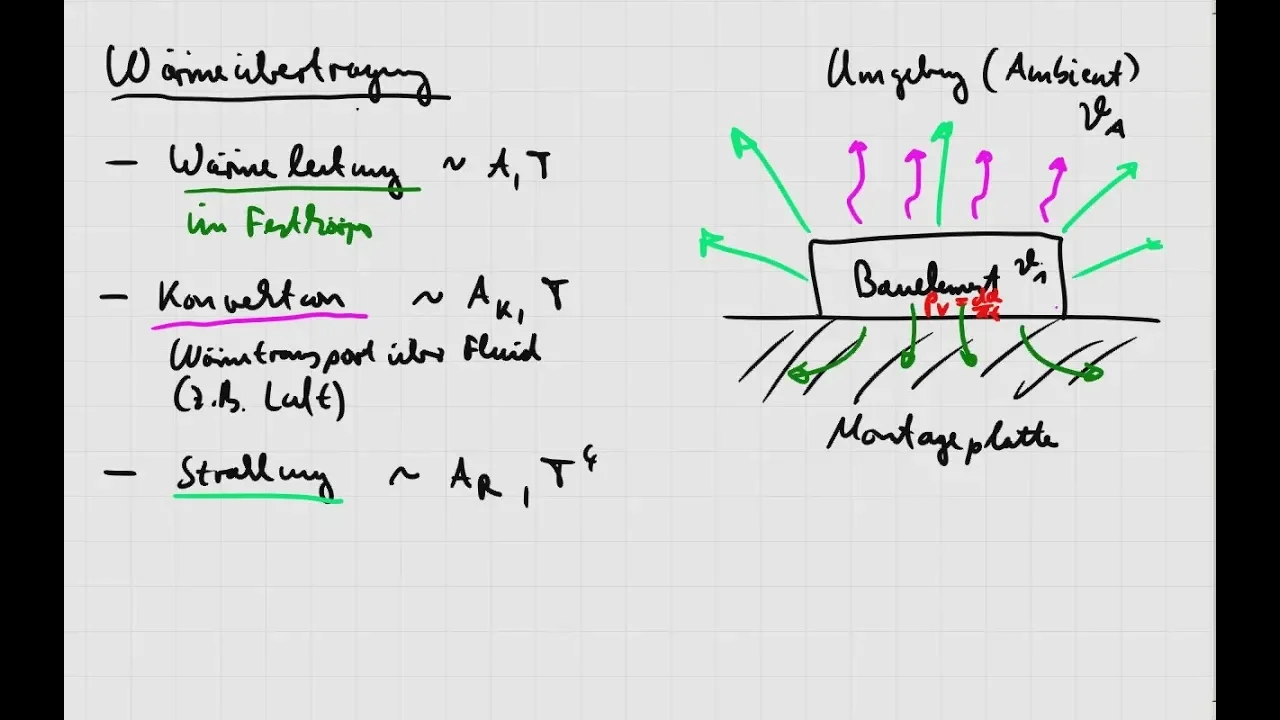
Added:Basic principles of heat transfer, specifically conduction, convection, and radiation in electronic systems.
Familiarity with 3D CAD modeling software and standard file formats such as STEP, IGES, and Parasolid.
Fundamentals of Computational Fluid Dynamics (CFD), including the concepts of fluid domains, boundary conditions, and volume meshing.
Understanding of basic electronic components and packaging, such as PCBs, integrated circuits, heat sinks, and fans.
Advanced mesh generation techniques specifically tailored for complex electronic assemblies and thin-volume geometries.
Defining thermal boundary conditions, transient heat loads, and contact resistances in CFD solvers.
Analyzing simulation results to optimize heat sink geometry, fan placement, and enclosure ventilation paths.
Exploring multi-physics simulations, such as structural-thermal-electromagnetic co-design for high-power electronics.
1.8K views9likes17:47Original Release: 2021-03-30
hello and welcome to simscales tutorial on cad best practices in today's session we'll take a look at one of the examples of an electronics enclosure we will run through some of the often encountered catfalls and how to solve them and finally take a look at some of the best practice guidelines that can be followed while designing the model for cfd simulation some of the basic cat faults that we encounter are intersections open volume and discontinuity by intersection if the cad model has multiple paths which are assembled together we should make sure that there are no overlapping entities and overlapping entities might end up in intersection and cannot be used for simulation an open volume might occur when the cad model has an open ending except intentional outlets or inlets this might also occur if there is a missing phase in your model or there are unnecessary gaps or holes in your model a discontinuity is something where there is a thin gap between the connected bodies or even the connected faces this might be the end product of production tolerances or design tolerances so these catfalls have to be fixed before starting a successful simulation let's take an example of an electronics enclosure and check if this model has any cat faults that we talked about initially a visual check should give you some of the obvious cad faults that is present in the model in our model we do have an enclosure and a set of internal components on a pcb let's take a look at the enclosure to see if there are any cut cat faults as you can see on the left bottom corner the enclosure is identified as a surface which means this will be imported as a seed body for a successful simulation seed bodies are not allowed all the entities or the components of your model should be a solid one let's see why the enclosure is identified as a surface on a visual check you could already see that the enclosure has a hole or a missing face at one of the corners we need to fix this to make sure the enclosure is detected as a solid body this can easily be done by selecting the edges of the hole or the gap and creating a new surface for all the cad operations i'll be using the onshape which is a web-based cad editing and creation tool all the operations done here for the for fixing the cad faults and also simplifying the model can easily be represented or replicated in other cad tools all right now that you have created the missing face in the enclosure you could already see that the enclosure is converted into a solid body let's hide the enclosure and check the internal components on the first look we could already see that the components are well modeled but if you take a deeper look you could already find out that there are intersections between several components with the pcb this has to be cleaned or fixed before starting the simulation there might be several interference in the model and hence it is better to check the interference for all the cad components in onshape this can easily be done by selecting all the components and running a check interference option the check interference should be available in most of the cad tools but in a different workflow when you run the operation to check interference we could already see that there are some of the red regions which are representing overlapping entities in our model we have overlapping entities between the connecting pins and the pcb and also one of the component is intersecting with the pcb to fix an interference this can easily be done using the boolean operations that is by subtracting or merging components with each other let's take an example of this connecting pin to solve the interference we need to apply the boolean operation and do a subtraction for tools we'll select the connecting pin and as a target we'll select the pcb board once when the operation is done you could already see that the interference is removed this can easily be verified by hiding the connecting pin and checking if the pcb board has a hole this makes sure this hole is going to accommodate the connecting pin thereby defining a clear contact between the two entities and also removing the interference if you check the other connecting pin which is interfering with the pcb when you hide it you might not see the hole on the pcb this means these two entities are overlapping so the boolean operation should be done for all the connecting pins let's move ahead and check the interference between the component and the pcb we already monitored that there is an overlapping region between the component and the pcb in this case we want to make sure the component is just touching the pcb and not interfering with it to do this again we'll select the boolean operation select the subtraction and this time we'll select the tool as the pcb and target as the component by running this operation you could already see that the component is cut down until the top face of the pcb thereby ensuring a proper contact between the pcb and the component and also removing the interference for an electronics enclosure type of analysis we need to make sure there are proper contact between the components for example if you have several components placed on a pcb we need to make sure there is a parallel or adjacent face touching the pcb and the component this in turn will make sure there is a automatic contact detection inside sim scale and there will be a proper thermal conductivity between these components now that we have fixed all the interference regions we'll move ahead and check for any other cat faults one of the catfalls that might be encountered often in all these electronics enclosure is discontinuity let's suppose there are components which are placed on pcb as we know that there should be a proper contact between the components and the pcb we have to check if there is any thin gaps between the components this can easily be checked by creating a section view and running through all the components you can already see that the smaller component which is orange in color is not touching the pcb you could see there is a thin gap between the pcb and the component this will prevent the automatic contact detection and hence there won't be any thermal contact between the pcb and the component to fix this we need to make sure we extrude the face of the component until the top face of the pcb once again these operations might be slightly different in other cat tools but would be easily replicable right now by extruding the component onto the until the pcb we are making sure there is a proper contact between the components we need to ensure this is this case with all the components of the pcb in our example we could already see all the other components are in contact with the pcb once all the overlapping entities are fixed we can again run the check interference operation to confirm if there are no other overlapping entities the second difference says that there are no interference detected in our model hence all the cad faults are fixed right now the components or the electronics enclosure is already ready to simulate from now on we'll just focus on some of the best practice guidelines that can be followed to make sure we'll get a good balance between the computational effort and the geometric details and the visual check should give you some of the obvious pointers for example you have the pcb board branding or the engravings on the pcb this is usually done on a design level to identify the pcb board as you can see these engravings are small solid regions or faces which might again encounter a huge or high mesh density which is not required for our cfd simulation as a best practice guideline whenever there is an engravings in a component or any pcb models you could simply remove them then we'll take a visual look to check if there are any unnecessary details that doesn't significantly contribute to the cfd simulation for example if you take the big component on the pcb there are certain fillets which are thin and will definitely increase the mesh size at these regions also these fillets are not going to affect the simulation accuracy significantly hence they can be removed apart from the fillets you could also see or check for any other small details that is not significant for the simulation for example this transistor model has some of the details which are done on the production level these features will not contribute to the simulation accuracy and can be removed a further best practice or simplification can be extruding this face until the top of the component this will make sure we don't have any fine mesh regions in these components now the component looks pretty much clean and ready to be simulated let's take a look at some of the other components for example let's take this component which is attached to the pcb using connecting pins in reality these connecting pins will be soldered to the pcb and hence these extruding parts below the pcb are just design features which can again be removed to remove this we need to split the connecting pins with the pcb and then remove the external or extruding regions let's first split the component for example we can take the bottom face of the pcb to split the connecting pins this will create additional solid regions in your geometry list this can simply be removed to make sure we don't have any high density mesh regions now let's take a look at one of the other components for example this component has the screws and bolts designed in it these are purely design features which are not significant for our cfd simulation and hence can be removed right now our model is cfd ready you can import this model and start your simulation now i have imported the fixed model into sim scale the first thing to do when you import a geometry model is to check on the geometry info this can be accessed by clicking on the importer geometry and selecting the drop down on the geometry info the geometry info will give you some of the information regarding the imported geometry such as format number of solid bodies number of seed bodies if anything present and other geometrical entities we need to make sure there are no seed bodies in our geometric or cad model and then we need to make sure the scaling is consistent to start an electronics enclosure simulation we need to do two more steps the first step would be to create a flow region or a fluid region inside this enclosure to account for the flow characteristics this can easily be done by clicking on the cad mode this will take you to the cad editing mode of simscale here you can do some basic operations on the cat but for our interest we will go ahead and create an internal flow region to do this you need to pick a seat face which means any internal face for example we are going to pick one of the internal face of the inlets and under boundary faces you need to pick the faces which are enclosing these openings for example the inlets are enclosed in this phase so this face should be picked for the boundary face and the on the other end there are some outlets which are enclosed with this boundary phase once when the boundary faces and the seat face is picked you can press apply this will create the blue colored flow region which is enclosing the air domain or the fluid domain of your model the next step is to actually make sure we have proper contact detection between all the components this can be ensured by running an imprint operation you could simply click on the imprint operation and press apply once when these two operations are done you could go ahead and click on the finish button on the top right corner this will create a copy of your model along with the fluid region and also the imprinting option now the model is ready and can be used for your simulation thank you you
Up Next

19:38
ANSYS Icepak & SpaceClaim: Fast Electronics Cooling CFD Workflow
@SingularityEngineeringLLC
61K views•2018-12-05

12:54
Triumph of Orthodoxy Icon: Byzantine Art & History Explained
@BenCallan
2.1K views•2024-08-06

9:49
FastAPI vs Flask vs Django: Choosing the Right Python Web Framework
@TechWithTim
302.5K views•2024-05-26

1:42
Game of Thrones Opening Credits: A Cinematic Analysis
@gameofthrones
46.3M views•2011-04-18
Related Study Plans & Knowledge Roadmaps
Structured learning paths in General & Interdisciplinary Studies
general-studies
Elevator Engineering: History, Physics & Cities
01From Hoists to Safety Brakes: The Dawn of Vertical Lift
02Hydraulic vs. Traction: The Engineering Physics of Elevators
03Modern Speed, Safety, and Algorithms
+ 2 more learning modules
12h5 modules
Explore Roadmap
general-studies
Rubber: Material Science, History & Geopolitics
01Origins of Natural Rubber & Mesoamerican History
02The Chemistry of Natural Rubber & Vulcanization
03The Geopolitics of the Rubber Boom & Colonization
+ 2 more learning modules
12h5 modules
Explore Roadmap
general-studies
Containerization: Evolution, Logistics & Trade
01Ancient Trade & Bulk Cargo: Amphorae to Barrels
02The Industrial Revolution & Cardboard Packaging
03The Containerization Revolution: Malcom McLean
+ 2 more learning modules
12h5 modules
Explore Roadmap
general-studies
Textile Tech: Evolution, Labor & Global Impact
01Pre-Industrial Textiles: Handloom & Cottage Industry
02Mechanization: The Spinning Jenny to the Power Loom
03The Factory System & Global Labor Transformation
+ 2 more learning modules
10h5 modules
Explore Roadmap