












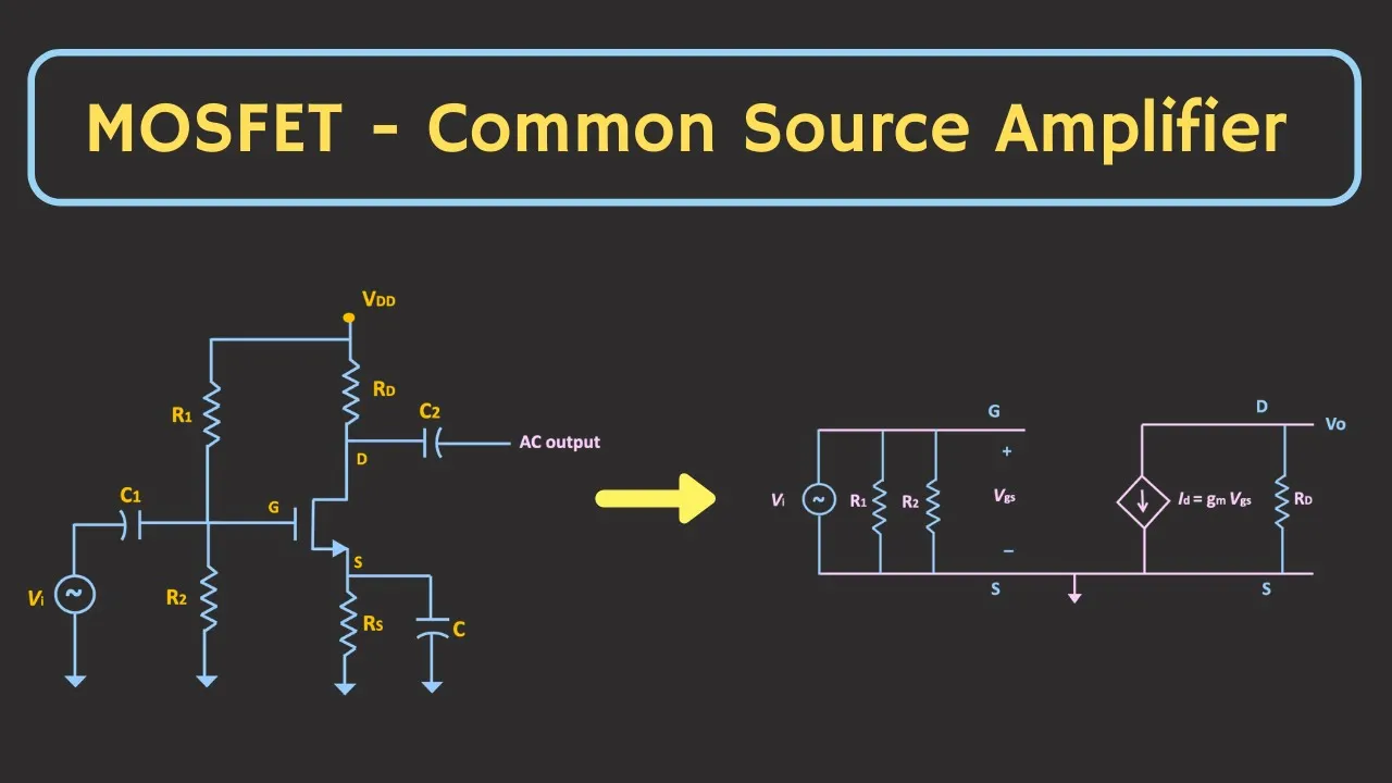







A MOSFET (Metal-Oxide-Semiconductor Field-Effect Transistor) is a four-terminal device consisting of a gate, source, drain, and substrate, where a voltage applied to the gate controls the formation of a conductive electron channel in the p-type substrate, thereby controlling the current flow between source and drain; this voltage-controlled resistance behavior makes MOSFETs essential components for building amplifiers and digital circuits.
Intro to MOSFETs: Structure, Operation, and Amplifier Applications
Added:Basic semiconductor physics, including p-type and n-type silicon, doping, and the behavior of P-N junctions.
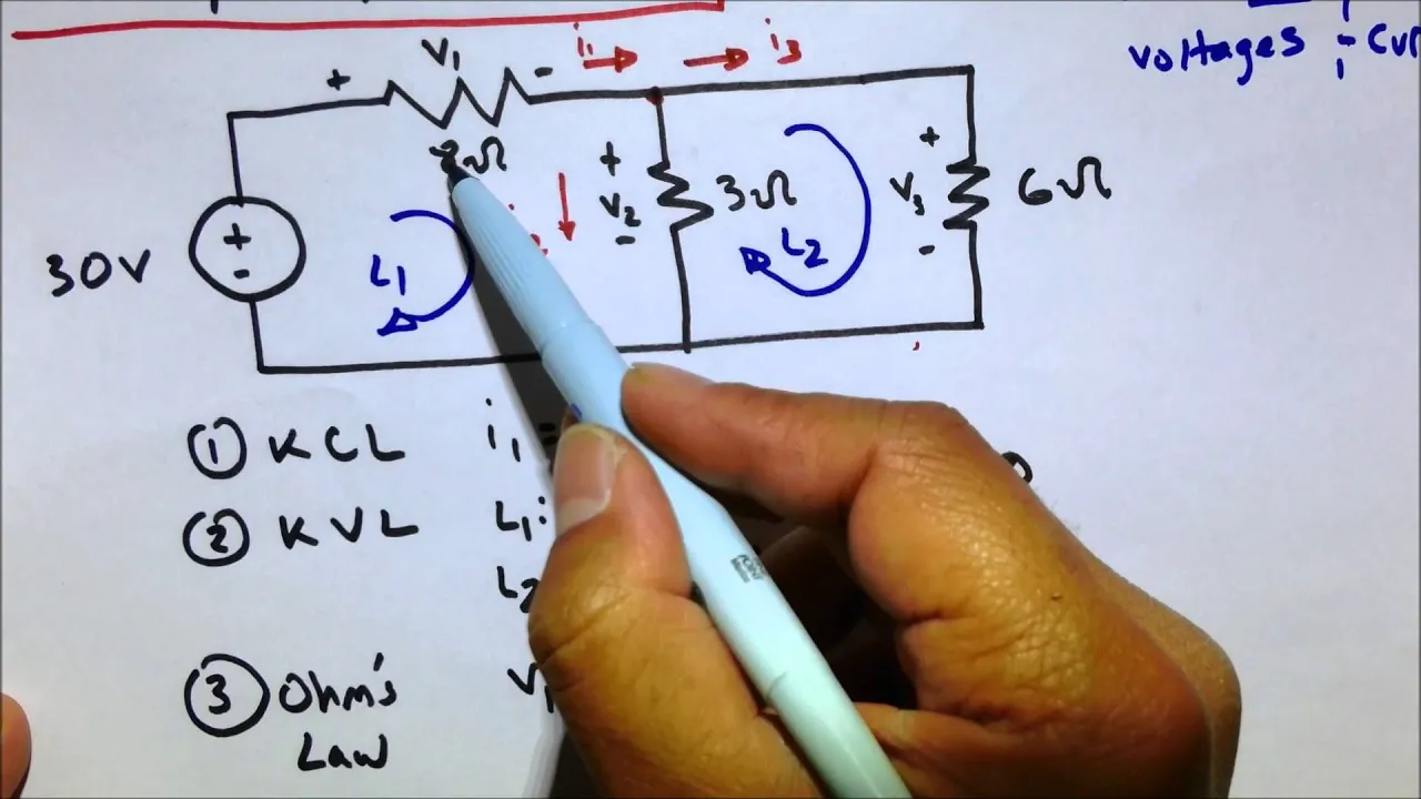
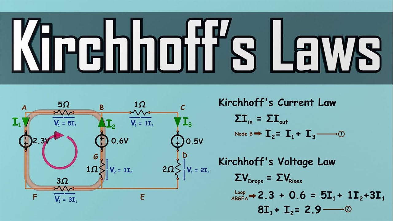
Fundamental circuit analysis concepts, specifically Ohm's Law, Kirchhoff's Voltage and Current Laws (KVL/KCL), and voltage dividers.
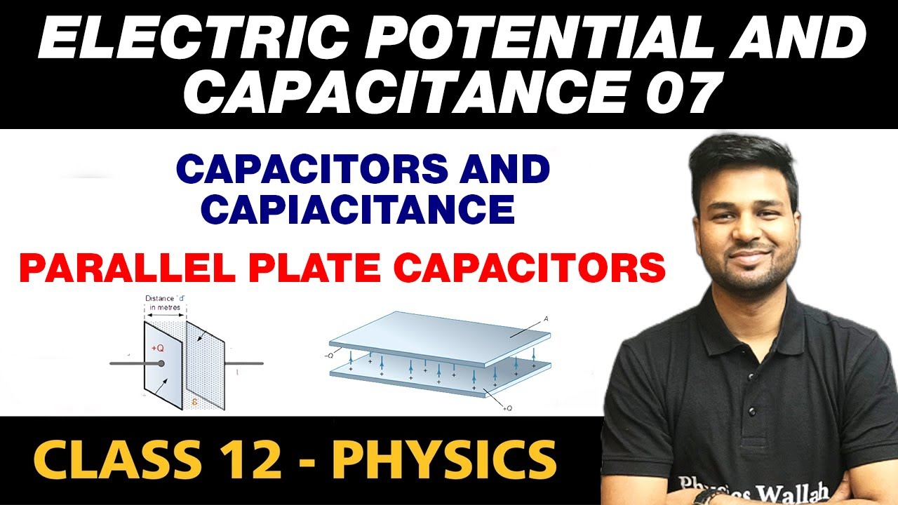
The concept of capacitance and electric fields, as the metal-oxide-semiconductor structure behaves like a parallel-plate capacitor.
An introductory understanding of diodes and basic transistor concepts (such as the difference between passive and active electronic components).
Mathematical modeling of the three main operating regions of a MOSFET: Cutoff, Triode (Linear), and Saturation.
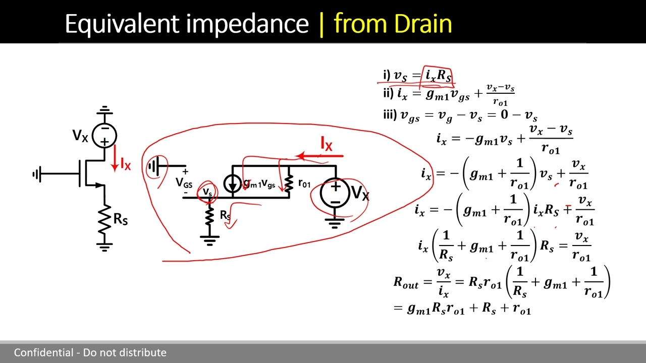
Small-signal analysis and modeling of MOSFET amplifiers (Common-Source, Common-Drain, and Common-Gate configurations).
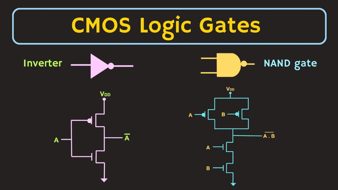
Complementary Metal-Oxide-Semiconductor (CMOS) technology and its application in digital logic gate design.
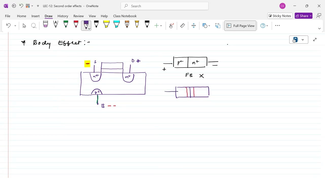
Non-ideal effects in practical MOSFETs, such as channel-length modulation (the Early effect), body effect, and subthreshold conduction.
335.2K views3.6Klikes1:04:50Original Release: 2014-11-11
[Music] Heat. Heat.
[Music] Heat. Heat.
[Music] [Music] Heat. Heat.
Heat. Heat.
[Music] [Music] [Music] [Music] Greetings. Welcome to electronic circuits one. I am Bzad Roavi and this is lecture number 29. Today we will begin our new adventure into CMOS devices and circuits. uh following our previous studies in uh diodes and other devices. Now I have designed these lectures so that you can avoid or you can skip the bipolar device and circuits lectures and directly come to this lecture and start learning about MOS devices. Uh so if you have skipped those lectures on bipolar devices and circuits, it's fine. you can start here without the need for those lectures. On the other hand, because of this, sometimes we have some repetition for those of you who have watched the bipolar device and circuits lectures. Uh but sometimes repetition is not that bad. It will also teach you some of the concepts again. So today we will uh start as follows. We'll take a look at the structure of the MOSFET. Uh see what it is. It's a new type of uh device a transistor and uh then we will go into its operation a little to just qualitatively understand how it works.
Uh our ultimate objective is to be able to derive current and voltage relationships for the device so that we can look at it as an electrical device not as some abstract physical device. In other words, we are hoping to build a circuit model for the transistor so that we can use it in the analysis and design of circuits, but it will take a while and we'll just go there step by step.
[Music] Uh this is a plot uh published by Gordon Moore who is one of the founders of Intel uh back in 1960s and in 1960s this is what he had observed. He said that it seems from a handful of data points that he had plotted here, the number of transistors per chip, per integrated circuit was doubling approximately every 18 months, every one and a half years.
And he said, well, this might continue.
this might go unstoppably and uh uh that was known eventually as Moore's law. Now what's amazing is that this trend never stopped. This trend started from early 1960s and has continued even today.
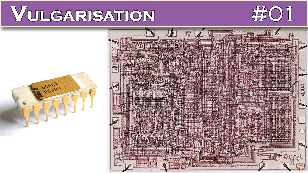
Uh so what we can see today is for example uh something like this where the number of transistors uh per chip for example in a microprocessor has gone from 2,300 in 1971 for the microprocessor 404 it was also from Intel to something on the order of billion transistors in most recent microprocessors.
Okay. So in a matter of 40 years 1971 to 2011 we have uh increased the number of transistors per chip uh from 2000 to let's say two billion. Okay. This is a phenomenal increase phenomenal uh progress in this technology and is unmatched by any other technology developed by human beings and that's why it has been uh responsible for such an explosive growth of semiconductors in our daily lives.
All right. Now uh when we build these chips we built them on a wafer. So this wafer is quite large today. And uh you can actually barely see the chips here.
So these are these are the chips. We build them on this wafer and then we dice it up and we collect the little chips and then we use them where whatever they are. They're microprocessors or there's something for your uh cell phone or something for your laptop etc. And uh this what is incredible about this technology is that this microprocessor here or this RF chip here has to have the same characteristics as this RF chip down here even though they are apart by something like 30 cm. the uniformity of this technology uh the ability to build transistors over here and transistors over here that are so close in characteristics is astonishing and that's the result of decades of progress in this domain.
[Music] So uh before we jump into the lecture I would like to pose one question or one suggestion. So, here's the first thing we want to do. Let's build an amplifier.
Okay. Why? Well, uh because we need later. How? Well, I will show you. Uh let's go and buy a voltage dependent current source. So here's a voltage balance current source that we have seen in basic circuit theory. In circuit theory, you typically denoted dependent sources by a diamond and independent sources by a circle. We don't make that distinction here. We just know from the context what they are. So uh this current source depends on this voltage between these two. Let's call this V_sub_1. And uh this current source is proportional to this voltage. So something times V_sub_1. Obviously, we need a coefficient here because we're going from voltage to current. So we'll just call that K.
All right. So we bought this.
And I'm hoping that I can build an amplifier using this voltage current voltage dependent current source. How did I do that? Well, here's a voltage that I would like to amplify.
We call VN.
Where does it come from? Well, maybe it's the sound coming from a microphone from this microphone that I'm wearing.
Or it's coming from an imager in the uh camera. For example, the camera that's capturing this image right now receives the light and based on that generates some voltage. So, uh this could be something, right? some signal I would like to amplify it.
Okay. Uh so what if I do this? What if I allow this current to flow through a resistor call it RL and I go ahead and measure the voltage across that resistor and I call it V out.
All right. And I'm hoping that from here to here I have an amplifier.
What do we mean by amplifier? We mean it generates an output that is hopefully larger than the input. Right? So if the input is a sinosoid like this, we should have a larger sinosoid at the output.
So let's see if that could happen. Well, uh we just need to solve this very simple circuit from basic circuit theory. We write a KCL right at this node.
Knowing that this voltage is called V out. So if the voltage across this resistor is called V out, the current through the resistor maybe I'll draw it like this. The current iss V out over RL. That's Ohm's law.
And now we can write a KCL at this node.
The this currents going out of the node equal to KV1.
This currents going out of the node equal to V out RL. They have to add up to zero. So we write k vub1 plus v out over rl equals z.
How much is v_sub_1?
Well, v_sub_1 happens to be vin in this particular implementation.
So I can say v out over rl equals minus k v in.
And that means V out is equal to minus K RL * V in.
Okay, we see that the output voltage the output sinosoid maybe is proportional to the input sinosoid obviously uh and this factor is some value. Maybe I can choose K RL to be a respectable number. maybe five, maybe 10. So I can build an amplifier that amplifies the signal at the input by a factor of 10.
Of course, uh there's a negative sign here which just came out of the equations. What does that mean? It just means that the output signal is flipped, right? Not a big deal. So if I have a sinosoid like this and I have some uh amplification factor of five, then it's five times bigger, but it's also flipped. So because it's flipped, it goes like this.
It's shifted by 180°. So that is the output voltage that we get when we apply this type of input voltage.
So the point of this exercise is to say that if we have a voltage dependent current source, we can build an amplifier.
And as we will see a MOSFET, a MOSS device can operate as a voltage dependent current source and can give us amplification. And amplification is essential to pretty much any electronic circuits that we build.
All right, so far so good.
Now before we introduce the MOS device itself, let's go and look at something much simpler just to get our feet wet and then we go to the MOS device. So here I would like to make a simple observation.
All right, we know how to build capacitors, right? We take a plate, a conductive plate, another conductive plate and that forms a capacitor and in between we have something could be air or it could be some other insulators.
Sometimes insulators are called dialectrics. So we can build a capacitor. So let's go ahead and do that. We build a capacitor.
Here's a conductive plate. So we say this is a conductive plate maybe made of metal or something and then uh you need other plate. Now for the other plate I will not use metal. I will use a piece of semiconductor maybe ptype semiconductor and I'll make it a little thicker just for illustration purposes. So this is a ptype piece of semiconductor.
I'm allowed to do that, right? This has some conductivity. It's not that bad.
It's not that great, but it's not that bad. So, this is a conductor and there's a conductor. So, we have a capacitor between them. And then in between, I will fill up with some sort of insulator.
So, this is insulator.
uh insulator uh sometimes we call it the dialectric dialectric okay so we have a capacitor right let's go ahead and apply voltage to this capacitor see what happens so here's a plate I make a contact here and I bring it to a voltage and then I make a contact to the bottom of this plate here and bring it to this voltage And I'll call this V1.
So we know that for example if we apply a positive voltage here, negative voltage here, then we will place some positive charge on this plate and some negative charge on this plate. Right?
That has to happen for a capacitor. So we'll uh change our color to red and place our charge positive here and negative here.
Okay. So what we see is that when the positive terminal of the battery is connected here and the negative terminal here, this positive terminal attracts some negative charge to this surface right here. What kind of charge is that?
Well, remember the ptype device, the ptype material has some electrons in it, some free electrons, right? Not a whole lot, but some. So it might be that we have a lot we have we get some of those electrons right here. They are free.
They are charge carriers. So we get some electrons here. And we'll have a name for these electrons. We will call these electrons channel the channel of the device. And we'll see why. So we have formed a channel in the device by applying a voltage between these two.
So far it just looks like a regular capacitor. Nothing exciting about it.
But the interesting thing is that we have some electrons here in this ptype material that are attracted to the closest uh possible surface to the other plate. They of course they need to come up all the way to this point.
Okay. All right. Uh so let me just uh make a couple of observations about this before we play with it. Uh what we know is that the charge that is stored on a capacitor is given by C * V right C * V1. So the capacitance of the structure times the voltage that we have applied from outside. So that is the amount of charge that we have positive charge on the top plate negative charge on the bottom plate.
Okay.
All right. Now, what happens if V1 increases? So, let's say B1 is a volt.
Now, it becomes 1.5 volts.
Well, we have more charge, right? So, we see that uh if V1 increases, Q increases.
If Q increases me means we have more positive charge here and more negative charge here. So the electron density here increases.
So electron density increases.
So I'll call this point A.
So far so good. All right, one more point which is less obvious but as interesting. So point the next point.
What happens if we bring these two plates closer to each other? We make this insulator thinner.
So I'll give it this a name. So let's just call this T for now for thickness.
If we reduce the thickness of this dialectric meaning the the gap if we reduce the gap what happens? So if t goes down what happens to the capacitance?
Well we know that if you have two plates and bring them closer to each other the capacitance of the structure increases.
So if t decreases and the voltage remains constant the capacitance increases.
Well it doesn't matter to what the voltage does anyway. So uh what we can say is that the capacitance increases.
If the capacitance increases and the voltage is constant what happens to Q? Q also increases.
So Q increases and that means that the electron density increases.
So electron density in the channel also increases.
So uh the interesting point here is that uh we have the ability to change the density of these electrons by changing this voltage. But also if you are interested in uh maximizing the electron density in the channel by construction we would like to minimize this thickness.
All right. So these are two little points that we need to remember for our later work.
Okay. So now let's go to the next step.
And the next step in addition to this voltage that I have applied between the two plates of the capacitor I come along and add another voltage source. Now here you have to be very careful not to get confused. So let me go ahead and do that. And let me change the color of my pen to avoid confusion.
So so this time the voltage I'm applying is from here to here.
Okay. So, I'll put a contact on this point. Bring a wire out. Put a contact on this point. Bring a wire out. And then apply a voltage source between these two terminals.
Positive here, negative here. We'll call this V2.
So, then what happens?
Well, we have some free electrons here and we have applied a voltage difference between this side and this side. So, the electrons start moving. They move away from the negative side and towards the positive side. So, electrons begin to flow this way through the battery and back. Right? So, we have a flow of current like so in electrons or the conventional positive current would be going this way.
Okay, that's not particularly exciting, but there's something interesting that we can observe. Okay, so we say that if V2 is applied, current flows from A to B.
A is here and B is here.
Okay. And by current I mean positive current. So positive current flows this way. Right?
Okay. So that's fine. But here comes the important point.
Let's suppose that we have set this up and everything's going uh there's some current flowing let's say 1 milliamp and now I come along and I increase V1 what happens? What happens to the current? If I increase V1 the electron density in the channel goes up. If the electron density goes up, uh the we have more electrons, we have less resistance between these two points. So the current that has to flow increases.
So that's the key idea here. If V1 increases, okay, my pen started acting up again.
If v_sub_1 increases then we know from previous uh analysis that the electron density increases. So electron density increases which means the resistance between a and b decreases. Right? And if you have more charge carriers, you have less resistance between two two points. So we have a resistance between A and B decreases which means current the current that's flowing increases.
So what's interesting is that a voltage connected between this plate and this plate V1 can control the current that flows from here to here or the electrons that go from here to here.
So it seems that we have something close to a voltage dependent current source, right? There's a current flowing from here to here and it depends on this voltage. There's a voltage between here and here and there's a current between here and here. So maybe it's a voltage dependent current source and maybe we can use it to build amplifiers and many other functions. So that is the first step towards learning how a MOSFET operates.
Okay. Now, uh let's go and look at the MOS structure.
Uh let me see if there's anything else that I need to mention. Okay.
All right. Well, we have we would like to build this structure. We're hoping that this will serve as a voltage dependent current source. But uh if you want to build this on that wafer that the guy was holding that wide thin wafer, we have some issues.
uh on a wafer we can only make connections to the devices from top of the wafer like so we can't go from the sides we don't have access to the sides of all these millions and billions of devices we can only attach from top so this contact is okay but then how about these two how about this one we can't go from the sides so we sort of have to stretch stretch this device so that these contacts can be made from the top of the wafer and that gives us the actual MOSFET structure. So let's go ahead and try to do that.
So we'll talk about the MOSS which stands for metal oxide semi conductor structure.
Okay. All right. So well we have the top plate here. Let's just draw it but draw it in three dimensions to make it clearer. So here's the top plate.
Uh it has some thickness.
We said this is a conductive plate, right? Like a capacitor.
So we call this uh uh the gate.
We will see why later. This is called the gate of the device. And the material is usually poly silicon.
Polysilicon is not an excellent conductor but it's a reasonable conductor. So we we use it as a conductive plate. In fact the name metal oxide semiconductor. This metal came about because a long time ago this was made of metal but now it's made of polyilicon. Although in future generations we may go back to metal. We don't know yet. But that's what we have.
Okay. So we built the top plate using polysilicon. Now we need an insulator.
So we will build some insulator underneath.
So this insulator is made of uh what we call oxide.
So this is really called this is really silicon dioxide but we just shorten it to oxide. We call it oxide. All right.
So we see the correspondence between this and this so far. We need a some sort of contact here to bring contact to the gate to bring a wire out. So put the contact here. Although in practice it may not be exactly here, but that's our contact. We have a wire connected to the gate.
Okay. Now we go to these points A and B.
So again we cannot contact from the sides. So we have to sort of stretch these so that we can access them from top. So let's stretch them. Why don't we do this? We stretch them like this.
We draw a line here and uh these will be these two points and then uh the rest of this bulk of this is under here.
So again if I try to draw it in three dimensions it looks like this.
Okay.
All right. So each of these have names has a name.
Uh this terminal which we call for example B now uh would have again a little contact to bring a wire out. This is called the source.
And in fact uh if this substrate this is called P substrate remember the ptype material that we had here we call it a P substrate and uh if this is Ptype substrate uh this area or which corresponds to for example B will made of N plus heavily doped N type material.
So why is it heavily doped and why is the end type? Well, it's heavily doped because we want to have a good contact between this wire that comes down and this part of the silicon.
If this is not N plus, you may get a some sort of diode or rectifying junction or something. So we don't we want to avoid that. That's why this is an M plus. Uh similarly, this one is N plus. And then again we have a little contact here and bring the wire out and call that the drain of the device.
So device so far has a gate, this big plate here, a source and a drain like these two except that they are moved up here, here and here. And uh then we have the contact down here. So again, we can't make a contact on the bottom. We have to bring it all the way up. So we put another little contact point here.
That's the contact that goes to the substrate. And uh to have a good connection between this wire and this P substrate, we place a P+ connection here, P+ doping here. And uh that is called the substrate.
A substrate connection.
All right. So a a few quick observations. Uh, number one, the MOSS FET.
By the way, FET stands for so MOS FET stands for field effect transistor.
field effect.
A transistor has four terminals, right? We have a gate, you have a source, a drain, and a subscript.
Sometimes the sub is called body, sometimes called bulk. Usually we call it the substrate.
Okay. So that presents some interesting uh challenges to us. Uh if we have studied only diodes which have only two terminals and resistors and capacitors and so on. Suddenly we come across a four terminal device. It seems much more complicated than before. For a two terminal device we had one current one voltage. That was it. Here we have four terminals. So we may have a current from here to here. We have voltage from here to here. all sorts of combinations. So we should not get scared. We'll just move forward and analyze it step by step.
All right. The second point that we can see is that uh moss structure is symmetric.
And by that we mean symmetric with respect to source and drain. Here's the source. Here's the drain. If you don't worry about the substrate for now, you can see that it's symmetric, right? You cannot tell which one is the source, which one is the drain.
And whether the substrate is over here or over here doesn't make any difference because we're just trying to make a connect wire connection to this big bulk here. Right? So that doesn't affect the symmetry that much.
Uh so the fact that the MOS structure is symmetric is sometimes actually very useful in circuit design.
All right. If you have watched the bipolar lectures, you might remember that a bipolar structure was not symmetric. So that's a point of contrast between the two.
Okay.
All right. So remember this t the the thickness of this insulator.
Well, that's this thickness here, right?
This thickness of this dialectric which we called oxide. So sometimes we denote this by T and then we add ox to be specific and that's from here to here we say t ox.
Now what we said was if T ox becomes smaller right it becomes thinner because the capacitance of structure goes up we have a greater electron density for a given voltage right and that's a very useful property that we have here so in technologies that have followed since more predicted what happens in 1960s until now this oxide thickness has been going down and down and down because we want to have a stronger control for this voltage upon this charge the mobile charge. You can intuitively feel that if this is a very thin layer then this voltage has a stronger effect on this uh this charge here. Right? So that's what has happened today. The oxide thickness is on the order of 15 to 18 anstroms.
A with a little circle on top. One angstrom is 10 the minus 10 m.
All right. Uh now a few other perspectives on this device. Because we don't want to draw all of this every time, we might draw just a two-dimensional view. So here's a two dimensional view. We draw it quickly. We have to get used to it. So here's our oxide. Here's our gate.
And here our source and drain. So N plus N plus source and drain.
And this is the P substrate.
In fact in many cases we may not even draw the substrate and in fact we may not even draw the substrate connection.
As we will see the substrate connection usually is some well- definfined voltage and we don't worry about it too much.
But you should always remember that a MOSFET fundamentally has four terminals even though we often don't draw this fourth terminal in our schematics or circuits etc. Okay. Now we also need some sort of circuit symbol because we don't want to draw this in every schematic. So the circuit symbol is like this. Uh you can see that this is the gate. So here's the gate and we have a an insulator. So we separate these by an insulator and then we put a line here and line here representing the source and the drain. We put an arrow on one of them and this forms our symbol.
Why do I have an arrow on one of them?
To indicate that that's the source. But I just said source and drain are indistinguishable. Well, yes and no.
Sometimes they are, sometimes they're not. The device is symmetric, meaning that sometimes they can be the source, sometimes this can be the drain. If we know what we mean by source and drain anyway, right? But for now, we'll just keep an arrow on this. In some other textbooks or some other classes, you might see that they don't draw an arrow here. They just draw don't draw anything here. And that's just a line here, a line here, and two lines to indicate the source and drain. But we usually draw the arrow and this arrow is pointing outward because this is a P substrate and these are N.
Okay. So this is what we call an N MOSFET. N type MOSFET and of course this is the gate. This is the source. This is the drain. What happened to the substrate connection? I don't didn't show it. If we insist on showing it because in some cases might be important then typically we draw a dashed line like so and that becomes the substrate connection. But in most cases in in this course we will not draw this.
We just have these three terminals.
All right. So that is the structure of the MOSFET and its symbol.
Okay. Now our job is to take this structure or this and play with it. We have a bit of idea how this works. We said that if we apply a voltage uh between these two terminals, between here and here, right? between here and here between A and B and we already have a channel of electrons a channel of electrons here or here then we may get a current right because uh the electrons prefer to go through this battery. So if we connect a voltage between this guy and this guy between source and drain we made get a current through source and drain the current will flow and what's interesting and important to us is that that current can be controlled by the gate voltage this voltage this voltage.
So if this voltage goes up and down of course with respect to here if this voltage goes up and down we control the density of electrons here. So if this voltage goes up and down. So there's a voltage source tied between here and for example here substrate right as this voltage goes up and down we adjust the density of electrons here meaning we reduce the resistance or we increase the resistance and that means that the current that will flow through source and drain and the channel through source and drain and the channel would be controlled by that voltage.
So these are some vague ideas that we have right now. we want to go in there and solidify these ideas step by step.
Okay. So let's go and add a page and start uh jump looking into the details of the circuit.
[Music] All right. So what I will do is u start.
So I would like to talk about MOSS operation here and uh I will draw the MOSS device uh for explain this operation. So what we will do for a while is that we draw the actual two-dimensional MOS device and apply some voltages around it and then we also draw the symbol for the MOS device and apply the same voltages around it and gradually we get used to looking at the symbol and understanding what the device is doing and eventually we don't draw the actual device structure anymore. We just draw the symbol just the way we did for P and junctions, right? We first we drew the whole P and junction and everything depletion region, but eventually we just drew the diode symbol for it. All right, so here's the structure. We have uh our gate and our oxide.
Uh then we have the source and drain areas and plus and plus and uh we have our gate and source and drain.
Okay. In the first experiment, we will connect the source to ground, the drain to ground, and we just apply one voltage source between the gate and the ground. So, we call this VG.
So, if I draw the symbol, that's what it looks like. Here's the symbol.
The source is grounded. The drain is grounded. And I have just applied a voltage between gate and ground. Right? VG.
We just want to see what's going on as this voltage varies. Maybe uh the device is not particularly useful right now, but at least we have we can see some of the operation.
Okay. All right. Well, let's start with uh uh choosing this VG slightly positive.
So, we make this gate more positive than all of these by some amount. Maybe 2 volts, maybe.3 volts, something along those lines. So, VG equals.2 volts.
Okay. So, what exactly happens? Well, let me just erase this because I need the space here. I will write that over here. So, VG equals.2 volts.
Well, remember the substrate here. In fact, what I have not shown is that the substrate is also connected to ground.
So, if you want to be careful, we draw a P+ for the substrate and we also connect that to ground. This is a P substrate material device.
All right. So this voltage is becoming more positive and we still recognize that we have a capacitor between this plate and this plate like what the the like the simplified structure I showed you earlier.
So as this voltage becomes more positive, it wants to repel positive charge here.
Do we have positive charge? Yeah, we have some holes. This is a ptype material, right? You have some holes.
So, the holes go away from this interface. This interface between the oxide and the silicon, the substrate.
And when the holes go away, what do they leave behind? Ions. Negative ions. So, we expose some negative ions here.
Okay. All over the place.
So I'll draw maybe another row here.
So these are negative ions.
This is reminiscent of what happened in a P and junction on the reverse bias in particular. Right? Remember that when we increase the reverse bias, we exposed more ions on each side, the depletion region became wider. So that's what we are thinking. If we apply 02 volts, uh we repel the holes. The holes go away.
They leave behind negative ions. And that's good. As far as this capacitor is concerned, this capacitor wants to have positive charge on this plate because we have a positive side of the battery. and then negative charge on this plate and that's negative charge.
So the capacitor is happy.
Okay. Uh so we have negative ions and we keep increasing this voltage and what we are thinking is that this these negative ions become more and more in population and we might actually call this a depletion region because it is depleted of free charge carriers. So we call this the depletion region.
Okay. All right. So, does this mean that if we just keep increasing this voltage, this dep region becomes wider and nothing else happens? No. That would be a really boring situation. That's not that interesting. What really happens is the following.
After a certain amount has reached for VG something else happens above and beyond form in the depletion region. So once VG reaches a threshold so a VTH which we called which we call the threshold voltage.
So once VG reaches a threshold voltage uh something else happens in addition to these ions being exposed. All of a sudden we will get some electrons right here.
So the capacitor is still happy because as we are increasing this gate voltage, we are hoping to place more positive charge here and more negative charge here. And previously the negative charge was coming only from negative ions. But now it's coming in addition from some electrons, some free electrons. Where these come from? Well, they can come from different sources. They can come from the substrate. Remember the substrate has some electrons or they can come from here. We don't worry about that at this point. But there will be some free electrons.
And so this is what we call the threshold voltage. The voltage at which we begin to introduce electrons here instead of these negative ions.
Okay. So now we begin to see some resemblance between this structure and the structure that we saw at the beginning. We saw that here. I said when this we apply a positive voltage here to the top terminal and negative voltage down here. We put some positive charge here and some electrons here and that's what we call the channel because it is capable of carrying a carrying a current right these electrons can move and they can conduct current. So what this means is that now that we have now that we have these electrons here, we have a channel of electrons. So they can conduct current just the way we did before.
So we call these the channel.
How much is the threshold voltage today?
about.3 volts maybe 4 volts maybe 2 volts depending on the technology that we are dealing with but something in that range.
Uh now of course one puzzling thing here is that uh how did we decide how did the device decide to stop exposing negative ions and instead bring free electrons.
Okay, that's beyond the scope of this course. For that you have to take some semiconductor physics understand how this works. But for now we'll just accept that as given and that's what happens. Below the threshold voltage if gate voltage the gate voltage is less than that we don't have electrons.
So we won't get any current from source of drain. But once the gate voltage passes the threshold we have some free electrons and the free electrons are capable of conducting current.
All right. So this is just the first step towards understanding how MOSFET works. We have a lot of things to cover but for now that's that's what we have.
All right. Let me look at my notes here.
Okay.
So now what happens as the gate voltage goes beyond the threshold voltage.
So what we see is that as uh VG increases just like the simple structure we saw before electron density the electron density in the channel density uh let me do this the electron density in the channel increases.
If the electron density increases, it is like we have a smaller resistance between these two, right? The channel is a better conductor, so we have less resistance.
Uh so uh it means that the resistance between the source which we denote by S and the drain which you denote by D is goes down.
Now that's a very interesting and useful device. What do we have here? We have a device like this. It's a resistor between source and drain. Right?
Here's source. Here's drain.
This is a resistor because we have some channel of conduction.
But this is a variable resistor. So it's it has a third terminal which we call the gate. And this gate can alter can vary the resistance between the source and drain. If the gate voltage is low, we don't have that many electrons. The resistance is high. If the gate voltage is high, we have lots of electrons. The resistance is low.
So that's a very useful device. This is called a voltage controlled resistor or voltage dependent resistor. A little different from a voltage controlled current source, but we'll get there.
Don't worry.
Okay.
All right. So we um we now can go and play with the device a little more. All right, the MOSFET has three terminals for now. We don't worry about the substrate that much. So we have three terminals and that means that we can apply a voltage here, apply voltage there, measure current here, measure current there. Right? It's a little more complicated than a simple diode.
All right, no problem. So why don't we do this? Let's go one step further and uh not assume that the source and drain have the same voltage.
We keep the source at ground but then we raise the voltage at the drain to see what happens.
All right. So uh assume vd the drain voltage is greater than vs the source voltage which is zero.
All right. So in cases like this we probably want to draw both the structure of the device and the symbol. We just do this for a while even though it might be tedious because we really want to get used to both of them and understand how they work. So here here it goes. We have our device with source and drain source grounded drain not grounded.
So drain is connected to some sort of voltage source VD and the gate is also connected to some voltage source which we call VG.
the substrate the substrate in case your curators is also grounded. Okay, so that's our structure and then at the circuit level this is what we have. We have our our MOSFET and the ground the source is grounded.
The drain is connected to a voltage source VD and the gate is connected to another voltage source VG.
We can do that.
Okay. So now what I need to do is vary VG.
See what happens. Vary VD. We see what happens. And to avoid confusion, we vary only one of them. So we keep one of them constant at the reasonable value and we vary the other one to see what happens.
For example, previously we assumed that VD was zero and we varied VG and saw that a channel begins to form and we exceed the threshold voltage and the resistance keeps going down and so on.
Now we have two voltages. So I I have the freedom I can select this to be variable and this to be constant or the other way around. And we have to do this very patiently to get used to all the characteristics.
Okay. So let's go ahead and first assume that VD is constant and we vary VG.
So case number one, VD is constant.
Uh for example, uh 3 volts.
Okay, just as an example. And we begin to vary VG. and we would like to see what happens. So I will draw that again and this time I'll play a trick on you.
I will turn this device counterclockwise by 90°.
So I will draw it like this VG and because the drain voltage is constant I will denote it by a battery.
So here's a battery and its value is.3 volts.
That's VD.
And I'm varying VG and I would like to see what happens. Now when I say what happens, what do I exactly mean? What am I looking for? Well, we're looking for any sort of current that flow can flow anywhere. Uh maybe see how those currents change. Remember for a diode we apply the voltage and measure the current. As the voltage went from let's say 0 to.8 volts we saw that the current started from zero and went up exponentially.
So maybe we have something similar here.
We would be good to test that.
Okay. So in this test uh we need to look at some currents. Let's look at the current that flows this way. This way here. Remember in the previous structure when we had a voltage difference between A and B and we had some electrons here.
We got a current going from this side to this side from A to B. So a same thing the same thing can happen here.
Uh and that's the current that flows here. It flows through this. We'll call this the drain current because it goes through the drain terminal. So we'll denote this by ID.
Uh so this is ID and this is ID.
This is called the drain current.
So I would like to plot ID as a function of VG.
VD is constant.3 volts. We don't touch it. We're just changing VG. So what do we expect? Here's VG.
Here's ID.
Okay, let's start with VG0 equal to zero.
When VG is equal to zero, uh this voltage is zero.
Well, VG is less than one threshold.
If VG is less than one threshold, we do not have electrons. We do not have free electrons. We don't have a channel. We don't have conduction. So, the current through the device is zero. No current can flow from here to here. No electrons can go from here to here. No positive current can go from here to here. So we say that ID is zero.
All right. So we keep increasing VG and we reach a threshold. So once we reach the threshold voltage VTH then we have electrons formed here. So we have some electrons and these electrons can conduct current.
So we begin to see a current flowing this way. your current flowing this way starts from the drain goes through the device through the channel goes to the source goes back to ground.
So we begin to see some current and as VG increases this current increases.
Why? Because as VG increases the resistance between the source and drain decreases.
So if I have a constant voltage here, if I have a constant voltage here and the resistance between the source and drain decreases, this current has to increase.
So this current increases.
Now we don't exactly know in what shape and form. Is it linear, nonlinear, etc. But at least we know it has to increase.
We'll just put some dots here because we don't exactly know what shape we will have.
So that's the called the drain current as a function of the gate voltage. In fact, we often call it as a as a function of the gate source voltage. So we look at as a voltage difference between the gate and the source between the gate and the source. You see this is connected between the gate and the source.
Okay. Now uh is there any other current device that we have to worry about?
Well, we have a current through the source you can call it is but as you can see the drain current and the source current are equal because if uh a current enters here it has nowhere else to go. It just goes all the way to the source and comes out. So the drain current and the source current are equal. So we rarely talk about the source current. We just talk about the drain current. If you're coming from the bipolar world, we don't have that defect of beta here. Meaning the collector current and the mirror current were not exactly equal here. The drain current and the source current are exactly equal.
Okay. Any other current sources? Any other currents that can flow? Can a current flow this way to the gate?
Well, if you go back to structure, we see that the gate uh plate, which is a conductive plate, is sitting on top of an insulator. After all, we're trying to build a capacitor. So, we don't expect any DC current at least to flow through this capacitor because we know for DC currents, capacitors are open. So, to the first order, we can say that the gate current is zero regardless of what's going on around the device. So, we will write that here. and we'll just remember it that IG is equal to zero.
Now in modern devices that's not exactly true. There's a bit of gate current but in this course we don't worry about it.
Okay let's go to case number two.
In case number two I will keep the gate voltage constant and reasonable. What's reasonable? uh maybe more than the threshold to keep the device uh to to have a channel. So we say VG is constant uh EG uh 1 volt.
So we want uh to have a a channel of electrons in the device. And now we vary uh the drain voltage. So I would redraw the circuit and I put a variable sorry I put a constant voltage source here a battery.
So here's a battery of value 1 volt and then I apply a variable voltage to the drain between the drain and the source really. So that's VD and again I would like to see what happens and by that we mean how does the current of the device change. We have only really a drain current. So that's what we're going to plot as a function of VD.
So we plot ID as a function of VD okay when VD is zero how much current do we have? Well, uh, if we have zero voltage across a resistor, we have zero current. Doesn't matter what the resistor is, right? The resistor can be high or low, but we have zero current.
So, no current here.
Uh, but so again, in your mind, you can place the resistor between these two points. When the channel is on, we said it looks like a resistor, right? There's a resistor between source and drain. And uh, as this voltage increases, this current wants to increase. So, this current begins to increase.
right away. There's no concept of threshold on this side, right? Because if the gate has a sufficiently positive voltage on it, there is already a channel of electrons here. And all we need to do is increase this voltage to increase that current. So we get something like that. And again, we don't know where it goes, etc. But that's the general shape of it.
All right. So this is called the ID VD characteristic. This is called the ID VG characteristic and they are distinctly different and they have mean they mean different things and we always play with these characteristics for a given device to understand its properties.
All right, our time is up. In the next lecture we will pick up from here and dive into the physics of the MOS device.
I will see you next time.
[Music]
Up Next

55:00
The Advanced Engineering Behind ASML's EUV Lithography Machines
@veritasium
18.2M views•2025-12-31
30:32
Ultrasonic Transducers: Resonant Frequency Measurement and Horn Design
@imajeenyus42
229.9K views•2017-02-22
54:16
Polymer Environmental Degradation: Mechanisms & Stabilization
@iit
1.8K views•2012-07-10
33:39
How a Student's Question Saved a NYC Skyscraper from Collapse
@veritasium
22.8M views•2025-04-26
Related Study Plans & Knowledge Roadmaps
Structured learning paths in Engineering
engineering
Building Acoustic Levitators: Physics & Arduino
01The Physics of Sound and Standing Waves
02Piezoelectric Transducers and H-Bridge Drivers
03Arduino Programming: Generating 40 kHz Signals
+ 2 more learning modules
14h5 modules
Explore Roadmap
engineering
Building Peltier Cloud Chambers: Particle Tracks
01Cosmic Rays & Cloud Chamber Physics
02Thermoelectric Cooling (TEC) Fundamentals
03Custom Liquid-Cooling Loop Design
+ 2 more learning modules
18h5 modules
Explore Roadmap
engineering
Yagi-Uda Antennas: Modeling, Build & VNA Test
01Introduction to RF and Antenna Fundamentals
02Yagi-Uda Antenna Design Principles
03Antenna Modeling and Simulation in 4NEC2
+ 2 more learning modules
18h5 modules
Explore Roadmap
engineering
ECG Monitor Design: Op-Amps, Filters & Noise
01Electronics & Breadboard Basics
02Op-Amps and Instrumentation Amplifiers
03Bioelectricity and ECG Fundamentals
+ 2 more learning modules
18h5 modules
Explore Roadmap