
























Barrier potential (or built-in potential) is the voltage difference that develops across a PN junction when no external bias is applied, created by the diffusion of charge carriers and the resulting separation of immobile ions in the depletion layer; it can be calculated using the formula V_B = VT × ln(NA × ND / ni²), where VT is the thermal voltage (approximately 0.026 V at room temperature), NA and ND are the acceptor and donor concentrations respectively, and ni is the intrinsic carrier density, with typical values of approximately 0.7 V for silicon and 0.3 V for germanium PN junctions at room temperature.
Barrier Potential & Built-in Potential in PN Junction Diode
Added:Basic semiconductor physics, including intrinsic and extrinsic (n-type and p-type) semiconductors and carrier concentration.
The physical mechanism of PN junction formation, specifically the diffusion and drift of charge carriers.
Concept of the depletion region (space charge region) and the creation of uncompensated immobile ions.
Fundamental electrostatic principles, such as electric fields, potential difference, and how charge separation relates to voltage.
Analysis of PN junctions under external biasing conditions (Forward Bias and Reverse Bias) and their effect on the depletion width.
The derivation and application of the Shockley Diode Equation (I-V characteristics) using thermal voltage.
Understanding junction capacitance (depletion and diffusion capacitance) and its frequency response.
The temperature dependence of diode characteristics, specifically how temperature affects thermal voltage and the built-in potential.
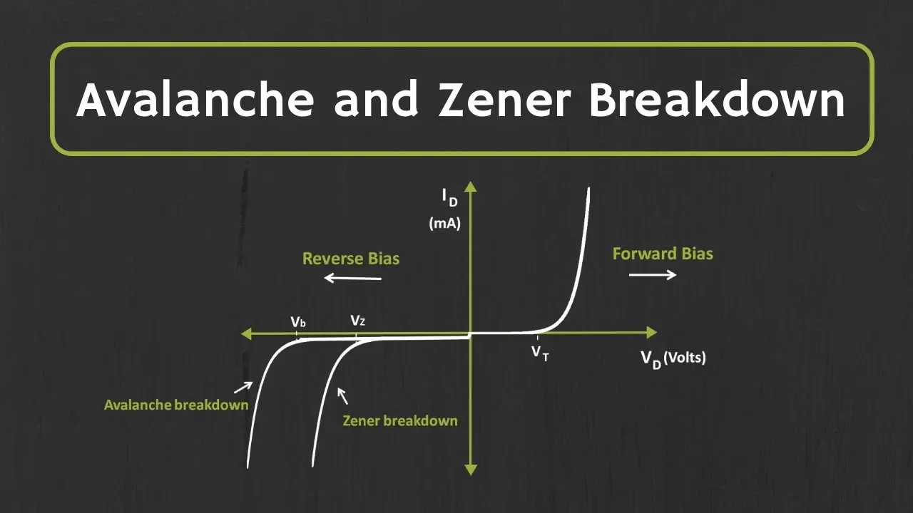
Exploration of breakdown mechanisms in diodes, such as Zener and Avalanche breakdown.
487.3K views5.2Klikes14:41Original Release: 2016-03-23
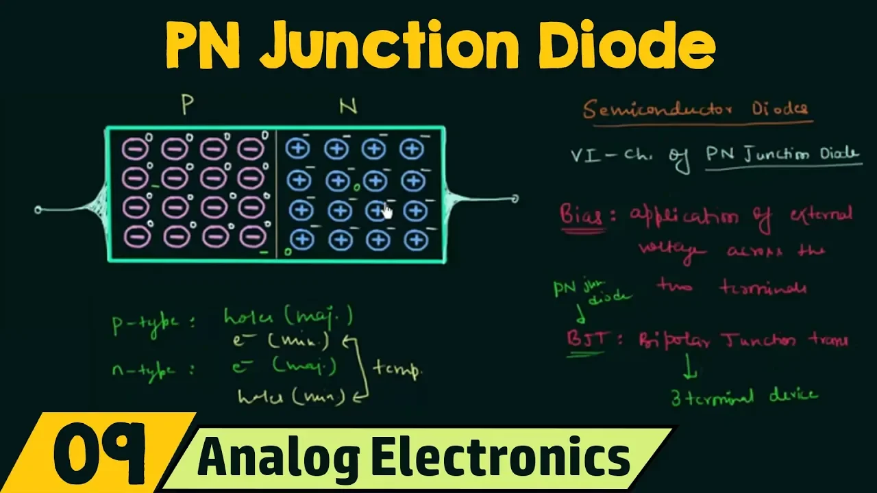
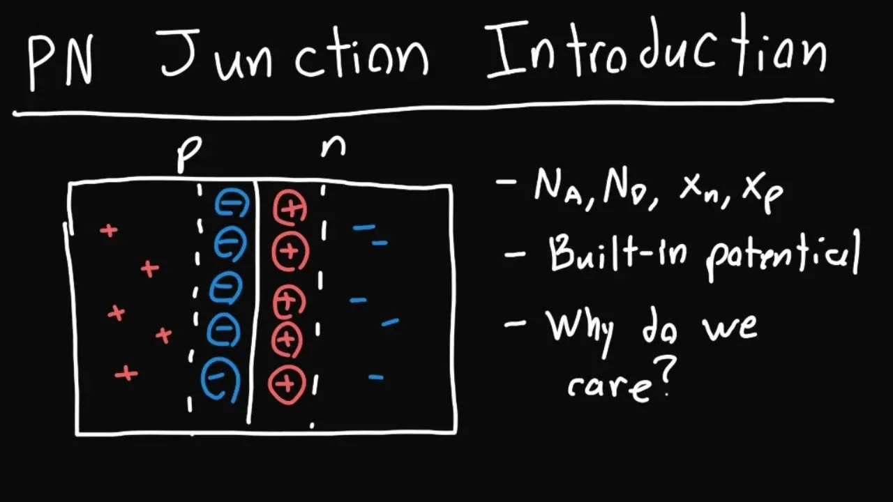
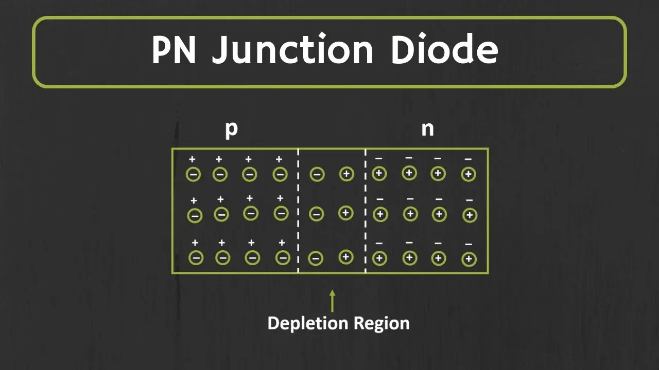
in the last lecture we completed PN Junction diode with no applied bias I explained by air potential in the same lecture and it is also called as built-in potential built-in potential in case of no applied bias we do not apply any external voltage source across these two terminals and because of diffusion we have depletion layer because of diffusion we have depletion layer now what is diffusion diffusion is the process in which free charge carriers or mobile charge carriers recombine with each other for example for example if we have immobile ion with hole and if this hole combines with electron then we have immobile ion with negative charge on the other hand if we have immobile ion with electron and if this electron combines with hole we have immobile ion with positive charge now why this immobile ion is having negative charge on it whereas this immobile ion is having positive charge on it because hole this hole is positively charged and this immobile ion is losing one hole so it will have one negative charge on it on the other hand electron is negatively charged and this immobile ion is losing one electron so it will have positive charge on it and if you see this if you see the depletion layer you will find on P side on P side we have layer of negative immobile ions because whole combined with electrons and on the N side we have layer of positively charged immobile ions because electrons combine with holes so this is how we get the depletion layer and it is called as depletion layer because it is depleted of free charge carriers we do not have mobile charge carriers in this reason we only have fixed immobile ions this whole process is also called as uncovering of immobile ions because when we have immobile ion and hole the charge neutrality is maintained when we have mobile ion and electron then also charged neutrality is maintained but when whole combines with electron or electron combines with whole the uncovering of charge carriers takes place and we have negatively charged immobile ion and positively charged a mobile ion and you can see the layer of negative immobilize and layer of positive immobilize act as the potential difference and this potential difference is called as barrier potential now why we are calling it barrier potential because it is acting as the barrier for the further movement of charge this positive layer here will repel the holes and this negative layer here will repel the electrons and because of this there is no further movement of charge therefore we call it barrier potential it is also called as built-in potential and in this lecture we will see the expression for building potential and we will also solve one numerical problem on it so if I draw the built-in potential or barrier potential then initially it is zero initially it is zero then it increases like this and the value the value is given by V subscript B V subscript B is barrier potential and we have to find out the expression for barrier potential V subscript B and it is equal to KT by E natural log in bracket we have na and D upon ni square so this is the expression for barrier potential and the derivation is not important in this course you only have to remember this formula we will use this formula to find out barrier potential this term this term KT by E is VT VT is the thermal voltage this is thermal voltage or you can call it voltage world age equivalent of temperature and V T is equal to K T by E we can easily calculate the value of VT and in numerical problems we will use the value of VT directly now what is K K is Boltzmann constant Boltzmann's constant and it is equal to one point one point three eight zero double six multiplied by 10 raised to power minus 23 joules per Kelvin so this is the value of Boltzmann constant and capital T here capital T here is absolute temperature absolute temperature and it is in Kelvin the unit for absolute temperature is Kelvin and if you have temperature in degree Celsius if you have temperature in degree Celsius and you want to calculate the absolute temperature then you can easily do it so this is how you can find the absolute temperature T dash is the temperature in degree Celsius and you have to add 273 to it and you will have your temperature in Kelvin this is a very basic thing to know for example for example if temperature is 27 degree Celsius it means T prime or T dash is equal to 27 degree Celsius to find out absolute temperature to find out absolute temperature it means capital T it is equal to 273 plus 27 and this will give us 300 Kelvin so in this way you can find out absolute temperature the next thing is small e small a small e is the charge of one electron charge of electron and it is equal to it is equal to 1.6 into 10 raised to power minus 19 coulomb so we are done with the terms involved in the volts equivalent of temperature or thermal voltage now we will see what we have inside this bracket and a and a is the exception acceptor concentration and D is donor donor concentration and Ni and I is intrinsic intrinsic carrier density so if we have all these things we can easily calculate the value for VB that is the barrier potential we will first calculate the value of V T the thermal voltage because we will use it directly in numerical problems it will save our time so first we will calculate V T so let's do it quickly VT is equal to KT by E and let's say the temperature T - it means the temperature in degree Celsius is equal to 27 degree Celsius this is the room temperature this is the room temperature and as we are performing the calculations at room temperature the value of VT is also valid for room temperature only K is equal to one point three eight zero double 6 multiplied by 10 raised to power minus 23 absolute temperature capital T is equal to 273 plus 27 and it is equal to 300 Kelvin so we have 300 here and the charge on one electron is 1.6 into 10 raised to power minus 19 and when you solve this you will get zero point zero two six volts so the value of VT is zero point zero two six and we will use this directly in numerical problem but there is one important thing this value of VT is valid for room temperature only this is valid room temperature only because when you change the temperature when you change the temperature this number here will change and the value of VT will also change but generally you will get questions in which the temperature is 27 degree Celsius or in question it will be given calculate the barrier potential at room temperature in that case we will take VT equals to zero point zero two six volts I will generalize this I will generalize this for any temperature T dash we will generalize this T is equal to 273 plus T dash and this is in Kelvin VT is equal to K KT by E T is equal to 273 plus T dash so we have 273 plus T dash I can write this as e by K 273 plus T dash e by K is 1 point 6 into 10 raised to power minus 19 divided by one point three eight zero six six multiplied by 10 raise to power minus 23 and when you solve this when you solve this you will get 273 plus T dash divided by one one six double zero so this is the generalized form of VT and if it is not the room temperature you can easily put the value of temperature here in degree Celsius and you will have the value of VT so I will modify the expression I will modify the expression this expression and V B is equal to VT natural log in bracket we have n a and D upon ni square so this is the formula we will use while solving the numerical problems let's move to the numerical problem and this problem we have to consider a silicon PN Junction a silicon PN Junction at room temperature now we have room temperature so we can say that value of VT is equal to zero point zero two six volts and it is doped at na equals to 10 raised to power 16 per centimeter cube value of n is equal to 10 raised to power 16 per centimeter cube and value of nd the donor concentration is equal to 10 raised to power 17 per centimeter cube an intrinsic carrier density it means ni is equal to 1.5 this is 1 point 5 into 10 raised to power 10 per centimeter cube so n I is equal to 1 point 5 into 10 raised to power 10 per centimeter cube and we have to calculate the built-in potential it means we have to calculate we beam this is very easy problem we only have to put the values in the formula so we'll do it quickly VB is equal to VT natural log in bracket we have n a nd by ni square VT is equal to zero point zero two six natural log n a is equal to 10 raised to power 16 so we have 10 raised to power 16 multiplied by 10 raised to power 17 and is equal to 10 raised to power 17 and I is 1 point 5 into 10 raised to power 10 so we have 1 point 5 into 10 raised to power 10 whole square 0.026 natural log 10 raised to power 16 multiplied by 10 raised to power 17 is 10 raised to power 33 1 point 5 square is to point to 5 into 10 raised to power 20 right or we can write it as we can write it as 0.026 natural log 10 raised to power 13 10 raise to power 33 divided by 10 raised to power 20 is equal to 10 raised to power 13 2.25 0.026 when you solve this when you solve this you will get twenty nine point one two three after multiplication we have zero point seven five seven volts and this is our answer so the barrier potential or built-in potential is equal to is equal to zero point seven five seven and this is for silicon PN Junction at room temperature and in coming presentations also I will use barrier potential for silicon equal to 0.7 volts and barrier potential for germanium equals to zero point three volts this is very important because we will use this a lot this is important and this is calculated at room temperature so this is all for this lecture in the next lecture we will discuss width of depletion region we will solve one numerical problem on width of depletion region so this is also in the next one
Up Next

27:08
Black Holes Explained: Structure, Detection, and Mysteries
@domainofscience
597.5K views•2021-08-22

12:53
21cm Hyperfine Transition in Neutral Hydrogen: Radio Astronomy Basics
@AaronRobertParsons
12.4K views•2011-10-13
15:55
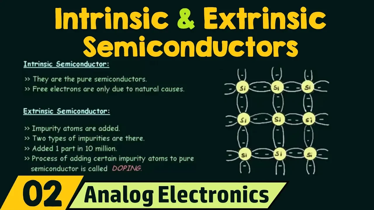
Intrinsic vs Extrinsic Semiconductors - Analog Electronics
@nesoacademy
746.1K views•2015-05-27

27:14
Entropy and the Second Law of Thermodynamics Explained
@veritasium
27.5M views•2023-07-01
Related Study Plans & Knowledge Roadmaps
Structured learning paths in Physics
physics
Nuclear Physics (Decay, Fission & Reactors)
01Atomic Structure and the Binding Force
02Radioactive Decay and Half-Life
03Nuclear Fission Mechanics and Chain Reactions
+ 2 more learning modules
12h5 modules
Explore Roadmap
physics
Soft Matter (Polymers, Colloids & Rheology)
01Foundations of Soft Matter & Thermal Forces
02Polymer Physics and Macromolecules
03Colloids, Surfactants, and Self-Assembly
+ 2 more learning modules
38h5 modules
Explore Roadmap
physics
Analytical Mechanics: Lagrangian & Hamiltonian
01Mathematical Foundations: Calculus of Variations
02From Newtonian Mechanics to Constraint Dynamics
03The Principle of Least Action & Lagrangian Mechanics
+ 3 more learning modules
28h6 modules
Explore Roadmap
physics
General Relativity (Spacetime & Cosmology)
01Foundations of Relativity: Special Relativity
02The Geometry of Spacetime: Equivalence Principle & Curvature
03Einstein's Field Equations: The Mathematics of Gravity
+ 2 more learning modules
55h5 modules
Explore Roadmap