Semiconductors like silicon have limited conductivity in their pure form but become highly conductive when doped with impurities: doping with pentavalent elements like phosphorus (5 valence electrons) creates N-type semiconductors where extra free electrons become majority charge carriers, while doping with trivalent elements like boron (3 valence electrons) creates P-type semiconductors where electron vacancies (holes) act as positive charge carriers; these two types work together in electronic devices like diodes.
N-Type vs P-Type Semiconductors Explained: 3D Animation
Added:Deep Dive
Basic atomic structure and valence electrons, specifically how outer-shell electrons dictate chemical properties and bonding.

Atomic Structure and Simple Electron Configuration Part 1
12.7K
Valence shell electrons are the electrons in the outermost energy level of an atom. These electrons are the only ones that participate in chemical bonding, while inner electrons do not participate in bonding. Elements with the same number of valence shell electrons have similar chemical properties. For example, all atoms with one valence electron have similar properties, and all atoms with two valence electrons have similar properties.
Click to watch →

C1.1 Lesson 4a Making Bonds (part1)
173
The number of electrons on the outer shell (valence electrons) determines the chemical properties of a substance. These outer shell electrons control how atoms react with each other and are responsible for chemical reactions because they are shared or transferred between atoms during bonding.
Click to watch →

MPSC Combine 2025 | SCIENCE | State Board Series | INSIDE THE ATOM | Basics to Advanced
6.8K
The valence shell is the outermost electron shell of an atom. Electrons in the valence shell are called valence electrons. The number of valence electrons determines an element's chemical properties and bonding behavior. For example, carbon has 4 valence electrons.
Click to watch →

Mole and Atomic structure : Chemistry | Theory with MCQs | NDA Crash Course
108.2K
Valence electrons are the electrons in the outermost shell of an atom that participate in chemical bonding. The number of valence electrons determines an element's chemical properties and bonding behavior. For example, nitrogen has 5 valence electrons in its outermost shell.
Click to watch →

Structure of Atom One Shot | ETT Cadre Science | By Kajal Ma’am
611
The valence shell is the outermost shell of an atom. Valence electrons are the electrons present in the valence shell. These electrons determine the chemical properties of the atom and participate in chemical bonding.
Click to watch →
Deep Dive
The crystal lattice structure of Silicon (or Germanium) and how these tetravalent atoms form covalent bonds.

JEE & NEET | Physics | Semiconductor | L02 | Devendra Kumar
1.5K
Silicon and germanium are tetravalent elements with four valence electrons. In their crystal structure, each atom forms four covalent bonds with neighboring atoms in a tetrahedral geometry. This creates a three-dimensional lattice where each atom shares electrons with four adjacent atoms.
Click to watch →

Semicinductors 2 Electrons and Holes By Prof. Harish Shasthri
266
Silicon and germanium are tetravalent semiconductors with four valence electrons. These electrons form covalent bonds by exchanging electrons with four neighboring atoms. Each silicon atom shares one electron with each neighbor, and receives one electron in return, creating four strong covalent bonds. This electron exchange strengthens the bonds, similar to mutual help between people. The crystal structure is continuous and extends throughout the material, with each atom having four neighbors.
Click to watch →

Semiconductors | Class 12th Physics | Farzana Parveen
9.2K
Silicon and germanium are Group IV elements with four valence electrons. They form covalent bonds by sharing electrons with neighboring atoms, creating a crystal lattice structure. This tetrahedral arrangement is fundamental to their semiconductor properties.
Click to watch →
12 Phy L14V2 | p-टाइप अर्धचालक, n-टाइप अर्धचालक | P-type semiconductor, N-type semiconductor
61K
Germanium and Silicon have 4 valence electrons each. In their crystal structure, each atom forms covalent bonds with 4 neighboring atoms, creating a stable lattice structure where all electrons are bound and no free electrons exist at absolute zero temperature.
Click to watch →

فيزياء السادس الاعدادي / الاستاذ كاظم العنكوشي / الفصل السابع / فيزياء الحالة الصلبة / المحاضرة 3
1.2K
Silicon and germanium atoms are tetravalent, meaning they have four valence electrons. To achieve stability, each atom must form four covalent bonds with neighboring atoms, sharing one electron with each neighbor. This sharing of electrons creates a stable crystal structure where each atom is bonded to four neighboring atoms through covalent bonds.
Click to watch →
Deep Dive
The fundamental classification of materials into conductors, insulators, and intrinsic (pure) semiconductors based on electrical conductivity.

Semiconductor easiest way|Class12Physics|intrinsic|extrinsic|#easyconcepts #exampreparation#12th
179
Materials are classified into three categories based on electrical conductivity: conductors (metals like copper, silver, aluminum) with high conductivity (~10^8 S/m) due to free electrons; insulators (rubber, glass, mica) with high resistivity (~10^8 Ω/m) and negligible free electrons; and semiconductors (silicon, germanium) with moderate conductivity between conductors and insulators. Intrinsic semiconductors are pure materials that show conductivity due to their own intrinsic charges without impurities. They have a diamond-like crystal structure where each atom forms four covalent bonds with neighboring atoms.
Click to watch →

MODERN PHYSICS L-4: MATTER WAVE AND ELECTRONICS
238
Materials are classified by electrical conductivity: conductors (high conductivity, e.g., silver, copper), insulators (very low conductivity, e.g., rubber, glass), and semiconductors (intermediate conductivity). In conductors, charge carriers are free electrons. In insulators, almost no free carriers exist. In semiconductors, charge carriers include both electrons and holes. Common semiconductors include silicon, germanium, and compound semiconductors like gallium arsenide. Intrinsic semiconductors are pure materials with low conductivity at room temperature. Extrinsic semiconductors are created by adding impurities (doping) to increase conductivity. This classification is fundamental to understanding electronic materials and devices.
Click to watch →
Lec 1-Ch1-Basics of Semiconductor-Semi-Conductor Physics-FE-SEM 2-MU-Admission Guruji
2.7K
Materials are classified into three categories based on their electrical conductivity. Conductors allow electrons to pass through easily, enabling current flow (e.g., gold, silver, copper). Insulators prevent electron movement, blocking current (e.g., rubber, plastic, glass). Semiconductors occupy the middle ground, with conductivity between conductors and insulators. Their conductivity depends on conditions like temperature, light, and impurity concentration. This classification is fundamental to understanding electronic materials and their applications in modern technology.
Click to watch →
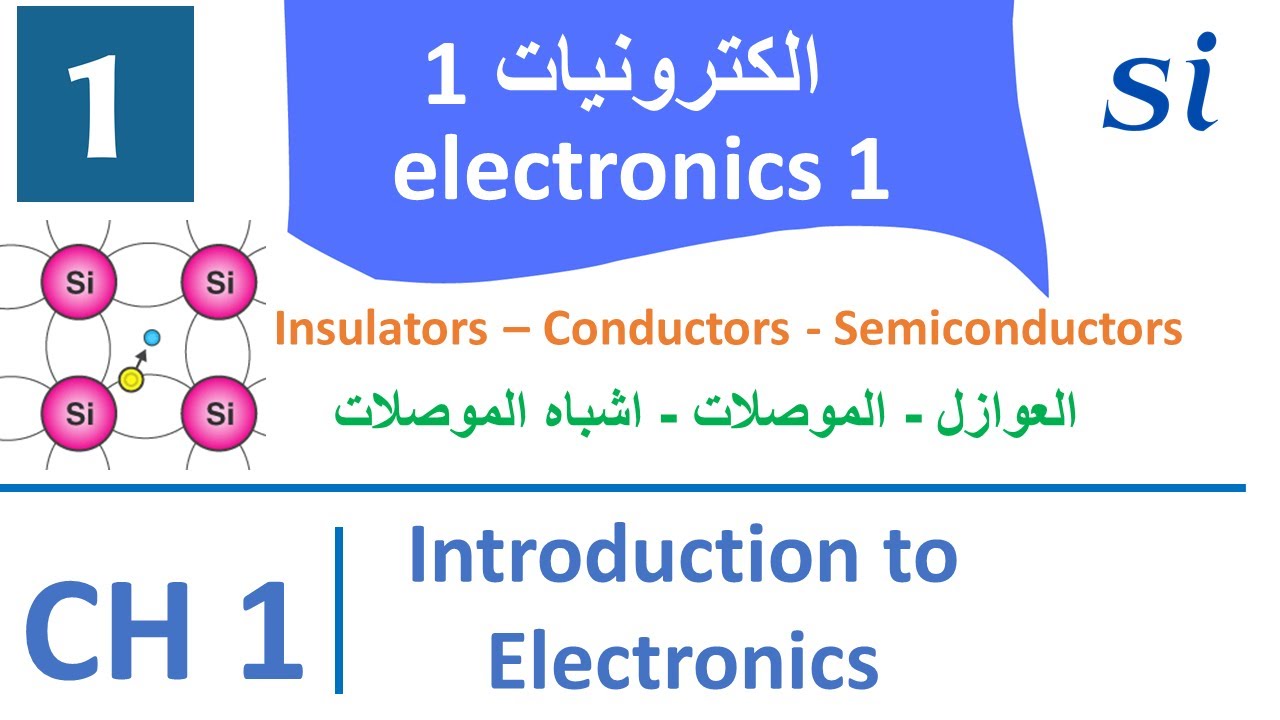
Part 4 | Insulators, Conductors, and Semiconductors | العوازل و الموصلات و اشباه الموصلات
7.5K
Materials are classified into three categories based on their electrical conductivity: (1) Conductors (موصلات) - materials that conduct electricity well, including metals like copper, aluminum, gold, and silver, which have one valence electron that is weakly bound and easily freed for conduction; (2) Insulators (عوازل) - materials that do not conduct electricity under normal conditions, such as rubber, plastic, glass, mica, and quartz, which have strongly bound valence electrons; (3) Semiconductors (أشباه الموصلات) - materials with conductivity between conductors and insulators, having four valence electrons, with silicon being the most commonly used semiconductor for manufacturing processors and transistors.
Click to watch →

Semiconductors
298
Materials are classified into conductors, insulators, and semiconductors based on their electrical properties. Conductors have abundant free electrons that allow easy current flow. Insulators lack free electrons and cannot conduct electricity. Semiconductors occupy the middle ground, having moderate conductivity. This classification is fundamental to understanding electronic materials. The key factor determining conductivity is the presence and mobility of free electrons, which can be influenced by temperature and material composition.
Click to watch →
Deep Dive
The basic concept of energy band theory, particularly the distinction between the valence band, conduction band, and the bandgap.

SSC JE 2023 | Basic Electronics - 01 | Semiconductor Physics - Part 01 | Electrical Engineering
38.3K
Energy band theory explains electrical properties of materials. The valence band is the highest energy band completely filled with electrons at absolute zero. The conduction band is the lowest energy band empty at absolute zero. The energy band gap is the energy difference between these bands, also called the forbidden energy gap because no electrons can exist in this region. In conductors, bands overlap (gap = 0). In semiconductors, the gap is 1.1-1.5 eV. In insulators, the gap is 10-15 eV.
Click to watch →

Energy band Diagrams I N and P type Semiconductor I Chapter 14 Semiconductor Class 12th Physics
59.5K
The valence band is the energy band formed by filled orbitals containing electrons, located at lower energy levels. The conduction band is the energy band formed by empty orbitals, located at higher energy levels where electrons can move freely. The energy gap (band gap) is the energy difference between the valence band and conduction band. This gap determines electrical properties: conductors have overlapping bands, semiconductors have small gaps (~1 eV), and insulators have large gaps (>3 eV). Electrons must gain sufficient energy to jump from the valence band to the conduction band for electrical conduction to occur.
Click to watch →
BCS12th-#183 NCERT ऊर्जा बैंड सिध्दांत | ENERGY BAND THEORY |
37.2K
When atoms are brought close together, their energy levels split into two distinct bands. The lower energy band is called the valence band, and the higher energy band is called the conduction band. The band gap is the energy difference between these two bands. The valence band is closer to the nucleus, while the conduction band is farther away. The band gap represents the minimum energy required for an electron to jump from the valence band to the conduction band.
Click to watch →
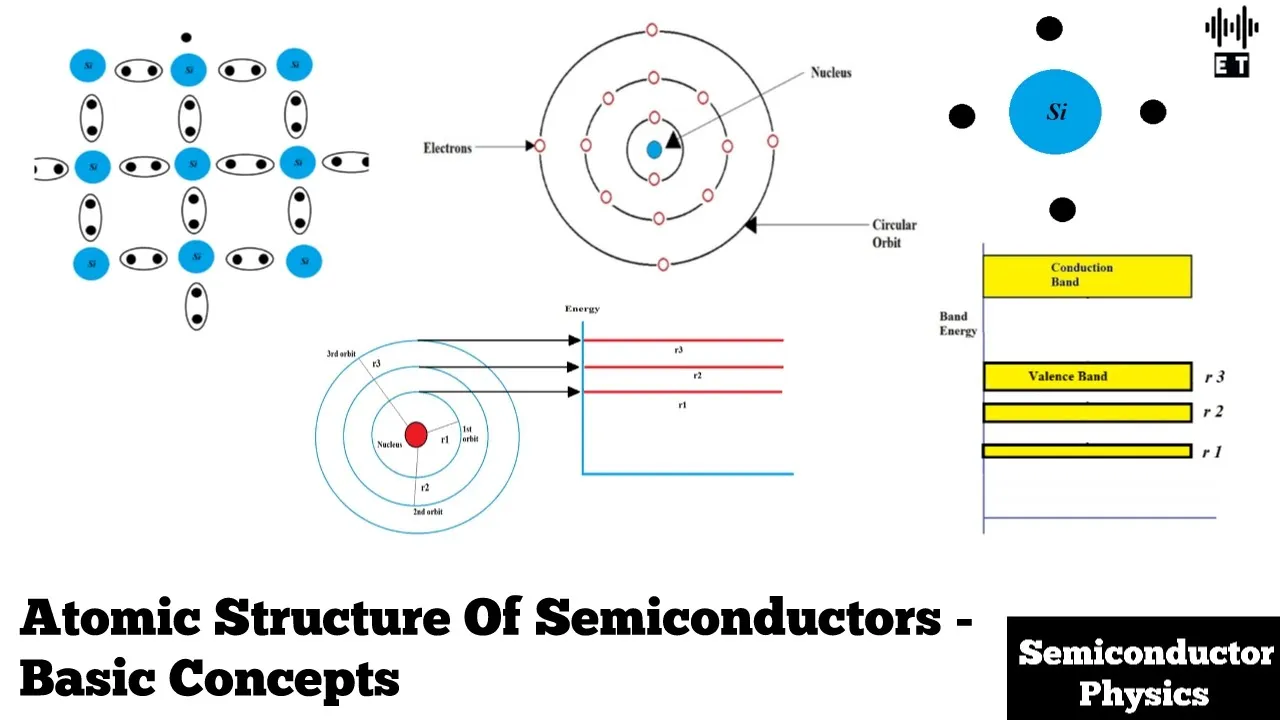
Atomic Structure Of Semiconductors | Basic Concepts | Semiconductor Physics
1.9K
Energy band theory describes three key components: the valence band (highest energy level occupied by valence electrons), the conduction band (energy range of free electrons that have escaped atomic bonds), and the forbidden energy gap (minimum energy required for electrons to transition between bands). These concepts explain how materials conduct electricity based on the energy barriers electrons must overcome.
Click to watch →
Energy band theory by systematic way to Physics
741
The valence band is the highest energy band that contains electrons at absolute zero temperature; it represents the energy level where valence electrons are located. The conduction band is the energy band above the valence band where electrons can move freely and contribute to electrical conductivity. The energy difference between these two bands is called the band gap. In conductors, the valence and conduction bands overlap, allowing electrons to move freely. In insulators, there is a large band gap that prevents electron flow. In semiconductors, the band gap is small enough that some electrons can gain sufficient energy to jump from the valence band to the conduction band.
Click to watch →
Prerequisite Knowledge
- Concept 01Basic atomic structure and valence electrons, specifically how outer-shell electrons dictate chemical properties and bonding.
- Concept 02The crystal lattice structure of Silicon (or Germanium) and how these tetravalent atoms form covalent bonds.
- Concept 03The fundamental classification of materials into conductors, insulators, and intrinsic (pure) semiconductors based on electrical conductivity.
- Concept 04The basic concept of energy band theory, particularly the distinction between the valence band, conduction band, and the bandgap.
Subsequent Learning
- Step 01The formation and physics of a P-N junction, including the depletion region and built-in potential barrier.
- Step 02The behavior of P-N junctions under forward and reverse biasing, leading to the operation of a semiconductor diode.
- Step 03The working principles of transistors (such as BJTs and MOSFETs) which stack N-type and P-type materials to amplify or switch electronic signals.
- Step 04The application of electron-hole dynamics in optoelectronic devices, such as Light Emitting Diodes (LEDs) and photovoltaic solar cells.
Core concept
N-type doping
P-type doping
Working together
Core concept
0:00Playing Section
- 1
Semiconductors form the basis of modern electronics.
- 2
They conduct electricity only under specific conditions.
Junctionless and Dopant-Free Transistors
While the traditional semiconductor paradigm relies on creating distinct, chemically doped N-type and P-type regions to form junctions, modern nanotechnology introduces 'junctionless' and 'dopant-free' electronics. At nanoscale dimensions, traditional chemical doping suffers from random dopant fluctuation, which causes severe performance variability and leakage. To overcome these physical limits, researchers have developed junctionless transistors that use a single, uniformly doped channel, eliminating PN junctions entirely. Additionally, 'electrostatic doping' uses external gate voltages to dynamically induce electron or hole channels in intrinsic (undoped) semiconductors only when needed. This alternative approach challenges the classical reliance on permanent chemical N-type and P-type doping, providing a more precise and scalable method for manufacturing next-generation microchips.
Deep Dive
The formation and physics of a P-N junction, including the depletion region and built-in potential barrier.

Semiconductors, One shot video for Class 12 Physics NCERT for CBSE 2024 Subscribe @ArvindAcademy
109.8K
A P-N junction is formed by joining p-type and n-type semiconductors in a single crystal. The junction is the boundary between the p-type and n-type regions. When a P-N junction is formed, majority carriers diffuse across the junction: electrons from n-side diffuse to p-side, and holes from p-side diffuse to n-side. This diffusion creates a region depleted of free charge carriers called the depletion region. The depletion region contains only immobile ions: positive ions on the n-side and negative ions on the p-side. This region has no free charge carriers to conduct current. The immobile ions create an electric field called the built-in electric field, pointing from the n-side (positive ions) to the p-side (negative ions). The potential difference across the P-N junction is called the barrier potential (Vb), approximately 0.7 V for silicon and 0.3 V for germanium at equilibrium. This barrier potential prevents majority carriers from diffusing across the junction and is responsible for the rectifying behavior of P-N junctions.
Click to watch →

فيزياء سادس علمي | الفصل السابع | الكترونيات الحالة الصلبة | الثنائي pn
84.7K
This section details the formation of the depletion region at the PN junction. When the diode is in equilibrium, electrons from the N-type region diffuse across the junction into the P-type region, leaving behind positively charged ions. Similarly, holes from the P-type region diffuse into the N-type region, leaving behind negatively charged ions. This creates a region depleted of free charge carriers on both sides of the junction. The separation of positive and negative ions creates a built-in electric field that points from N to P, and a corresponding built-in potential barrier that prevents further diffusion of charge carriers.
Click to watch →

فيزياء السادس العلمي /الفصل السابع / المحاضرة 5 / الكترونيات الحاله الصلبة#الفيزيا_تبقى_حلوة
21.1K
A P-N junction is formed by joining P-type and N-type semiconductor regions. The P-type region is doped with trivalent impurities (like boron) creating holes as majority carriers, while the N-type region is doped with pentavalent impurities (like antimony) creating electrons as majority carriers. The junction interface is coated with metallic material for electrical connections. The depletion region forms when majority carriers diffuse across the junction: holes from P-type diffuse into N-type, leaving positively charged acceptor ions, while electrons from N-type diffuse into P-type, leaving negatively charged donor ions. This creates a charge-depleted region on both sides. The separation of positive and negative ions generates an electric field directed from P to N, creating a built-in potential barrier. The barrier potential depends on the semiconductor material (silicon: ~0.7V, germanium: ~0.3V at room temperature), dopant concentration, and temperature. This potential barrier prevents further diffusion of majority carriers and is fundamental to the rectifying behavior of P-N junctions.
Click to watch →

Semiconductor (अर्द्धचालक) | Agniveer Airforce Physics Class #43, Navy SSR Physics Class
31.1K
A PN junction forms when P-type and N-type semiconductors are joined. Majority carriers diffuse across the junction: holes from P-side move to N-side, and electrons from N-side move to P-side. This creates a depletion region depleted of mobile carriers with a built-in potential barrier. The barrier potential opposes further carrier diffusion and is fundamental to diode operation.
Click to watch →
Semiconductor | Physics For CUET 2025 | CUET SAFAL 3.0🔥
192.7K
A P-N junction forms when P-type and N-type semiconductors are joined. Electrons diffuse from N to P while holes diffuse from P to N, creating a depletion layer depleted of mobile charge carriers. Fixed ions remain: positive in N-type and negative in P-type regions, creating an electric field opposing further diffusion. The barrier potential is 0.7V for silicon and 0.3V for germanium. Forward bias (positive to P, negative to N) reduces barrier potential and depletion width, allowing current flow. Reverse bias (positive to N, negative to P) increases barrier potential and depletion width, blocking majority carrier flow. Donors donate electrons, acceptors accept electrons, creating the fixed charges.
Click to watch →
Deep Dive
The behavior of P-N junctions under forward and reverse biasing, leading to the operation of a semiconductor diode.
P - N JUNCTION FORWARD & REVERSE BIAS, ACTION OF P - N JUNCTION SEMICONDUCTOR DIODE. 07
280
A P-N junction diode conducts current in forward bias when the positive terminal of a battery is connected to the P-side and negative to the N-side, reducing the potential barrier and allowing charge carriers to diffuse across the junction; in reverse bias, the connection is reversed, increasing the potential barrier and preventing current flow, making the diode act as a one-way switch. The potential barrier for silicon is approximately 0.6-0.7V and for germanium is 0.3-0.35V.
Click to watch →

Electronics | इलेक्ट्रॉनिकी | L12 | Complete Unit 09 | MPPSC 2021/22 | Shubham Gupta
79.1K
A PN junction forms when P-type and N-type semiconductors join. At the junction, a depletion region forms where charge carriers are depleted. Forward biasing (positive to P-type, negative to N-type) allows current flow. Reverse biasing (connections reversed) prevents current flow. This one-way valve behavior is essential for diode operation and forms the basis of all semiconductor devices.
Click to watch →

Electronics_EP.4-Semiconductor and Introduction diode
118
When P-type and N-type semiconductors are joined, a P-N junction forms with a depletion region containing few charge carriers. Forward bias (positive on P-side, negative on N-side) narrows the depletion region and allows current flow. Reverse bias widens the depletion region and blocks current. This asymmetric behavior enables diodes to control current direction. Silicon diodes require 0.7V forward voltage to conduct, while germanium diodes require only 0.3V.
Click to watch →

P N Junction Diode in Hindi
213
This section explains the operation of PN junctions under forward and reverse bias conditions. In forward bias, the P-type region connects to the positive terminal and N-type to the negative terminal, reducing the barrier potential. When the applied voltage equals the built-in potential, the barrier is eliminated, allowing majority carriers to diffuse across the junction easily. The current increases exponentially with applied voltage, following the diode equation I = I_s(e^(V/V_T) - 1). For silicon diodes, the forward voltage drop is approximately 0.7V. In reverse bias, the P-type connects to the negative terminal and N-type to the positive terminal, increasing the barrier potential and widening the depletion region, preventing majority carrier flow. This asymmetric behavior enables PN junctions to function as diodes in electronic circuits, allowing current to flow in one direction while blocking it in the opposite direction.
Click to watch →

Class 12 Physics Chapter 14 One Shot| Ardhchalak One Shot| Ardhchalak Class 12 Physics Imp Questions
32.5K
A PN junction diode operates in two modes: (1) Forward bias - P-type connected to positive terminal, N-type to negative terminal. This reduces barrier potential, narrows depletion region, and allows current to flow easily (milliampere range) due to majority carriers crossing the junction. (2) Reverse bias - P-type connected to negative terminal, N-type to positive terminal. This increases barrier potential, widens depletion region, and blocks current flow (microampere range) due to minority carriers. The VI characteristic curve shows current increasing rapidly in forward bias and remaining small in reverse bias until breakdown voltage is reached.
Click to watch →
Deep Dive
The working principles of transistors (such as BJTs and MOSFETs) which stack N-type and P-type materials to amplify or switch electronic signals.

Fonctionnement des transistors MOSFET et BJT
2.4K
When N-type and P-type materials join, a depletion zone forms with a 0.5-0.7V potential barrier. Forward bias reduces this barrier, allowing current flow; reverse bias widens it, blocking current. BJTs use this principle: NPN transistors have emitter-base-collector regions where a small base current controls a larger collector current through electron diffusion across the base region.
Click to watch →
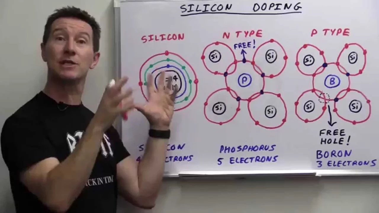
EEVblog #748 - How Do Transistors Work?
298.8K
Transistors function as electronic switches or amplifiers through semiconductor physics: BJTs use current-controlled operation where a small base current enables a large collector-emitter current via electron-hole recombination in doped silicon layers, while MOSFETs use voltage-controlled operation where an electric field across an insulating gate creates a conductive channel without gate current flow; both types rely on doping silicon with impurities (phosphorus for n-type, boron for p-type) to create charge carriers (electrons and holes) that enable current flow when appropriate voltages are applied.
Click to watch →
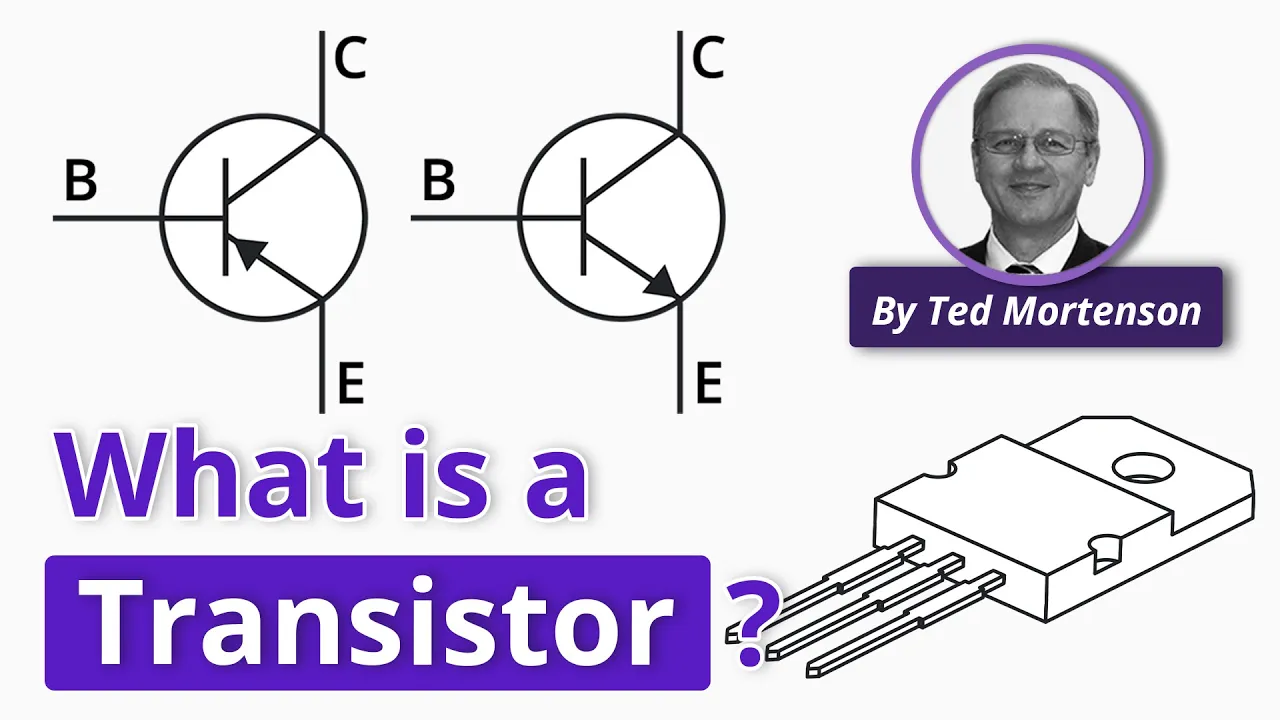
What is a Transistor | Working Principles
281.5K
A transistor is an electronic component used to amplify or switch electronic signals and electrical power. The name derives from combining 'transfer' and 'resistor.' Transistors are found in virtually all modern electronics, with phones containing hundreds of thousands and computers containing millions. The bipolar junction transistor (BJT) is the most common type, consisting of three semiconductor layers. Silicon is the primary material, with germanium being an alternative. The manufacturing process involves doping—introducing impurities to create P-type (positive) and N-type (negative) regions. BJTs come in two configurations: NPN and PNP, each with distinct electronic symbols featuring an arrow indicating the emitter-base connection direction.
Click to watch →
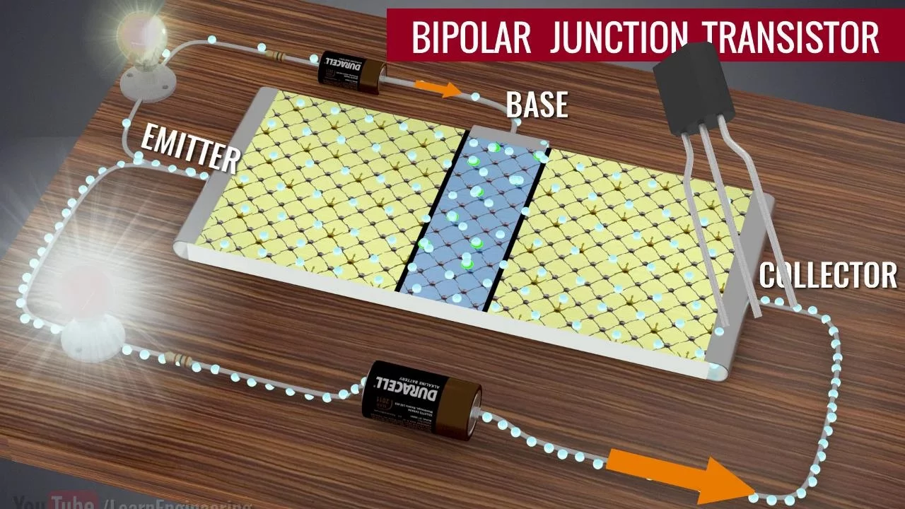
Transistors, How do they work?
9.5M
A Bipolar Junction Transistor (BJT) is a three-layer semiconductor device (NPN or PNP) that functions as both an amplifier and a switch by controlling the flow of electrons between its emitter and collector through a small base current; the BJT operates based on the principle of doping silicon with impurities to create N-type (excess electrons) and P-type (electron-deficient holes) regions, where applying forward bias to the base-emitter junction allows a small base current to control a much larger collector current, enabling signal amplification and binary switching operations essential for modern electronics.
Click to watch →

🔥FEEE || एकदम शुरू से || 2ND SEMESTER || ONE SHOT || BY-RAHUL SIR
106.9K
A Bipolar Junction Transistor (BJT) is a three-terminal device (Emitter, Base, Collector) that controls current flow and amplifies signals. NPN has two N-type layers with P-type in between; PNP has two P-type layers with N-type in between. The base current controls a larger collector current (Collector Current = Beta × Base Current). A Field Effect Transistor (FET) is a voltage-controlled three-terminal device (Source, Drain, Gate) that controls current flow using voltage. MOSFET (Metal Oxide Semiconductor FET) has an insulating oxide layer between gate and channel, providing very high input impedance. FETs are used in amplifiers, switching circuits, and digital electronics.
Click to watch →
Deep Dive
The application of electron-hole dynamics in optoelectronic devices, such as Light Emitting Diodes (LEDs) and photovoltaic solar cells.
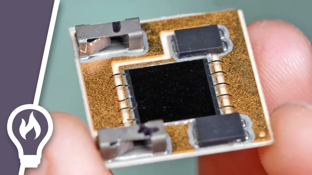
How diodes, LEDs and solar panels work
855.5K
This section explores how diodes enable light emission and energy conversion. LEDs emit light when electrons fall into holes, releasing energy as photons whose wavelength depends on the band gap energy. Solar cells reverse this process: photons eject electrons, creating electron-hole pairs separated by the depletion zone's electric field to generate voltage. Material selection determines output: silicon produces infrared, gallium arsenide phosphide creates visible colors, and gallium nitride enables blue light due to its larger band gap requiring more energetic photons.
Click to watch →

AYT FİZİK KAMPI-30 (MODERN FİZİĞİN TEKNOLOJİDEKİ UYGULAMALARI, YARIİLETKEN, LASER)
71.9K
Transistors are three-terminal semiconductor devices (emitter, base, collector) that can amplify signals or act as electronic switches. A small current at the base controls a larger current between emitter and collector, making transistors fundamental to computers and amplifiers. Transistors come in NPN and PNP types, with current flowing in opposite directions. LEDs (Light Emitting Diodes) convert electrical energy directly to light through electron-hole recombination at p-n junctions, offering low power consumption and long lifespan. Solar cells (photovoltaic cells) convert light energy to electricity using semiconductor junctions - photons excite electrons, creating electron-hole pairs separated by the built-in electric field. Larger surface areas capture more light and generate more electricity.
Click to watch →

L-8, जैनर डायोड एवं ऑप्टोइलेक्ट्रॉनिक डिवाइस | Zener Diode & Optoelectronic Devices | अध्याय-14
23.1K
Optoelectronic devices work with light, either detecting or emitting it. Photodiodes detect light through the photovoltaic effect. When light falls on the p-n junction, photons break covalent bonds, generating electron-hole pairs. Under reverse bias, the built-in electric field separates these carriers, causing them to flow through the external circuit. The generated current is proportional to light intensity. The V-I curve is plotted in the third quadrant. Higher light intensity produces higher current, allowing photodiodes to detect and measure light intensity. LEDs (Light Emitting Diodes) convert electrical current to light in forward bias. When current flows, electrons from the conduction band recombine with holes in the valence band, releasing energy as photons. The color depends on the band gap energy. LEDs cannot be made from silicon or germanium because these produce infrared light. For visible light (350-700 nm), band gap must be 1.8-3.0 eV. LEDs are made from gallium arsenide phosphide (GaAsP) with different arsenic-phosphorus ratios producing different colors. For red light, the ratio is approximately 0.6 arsenic to 0.4 phosphorus. LEDs have advantages over traditional bulbs: lower cost, longer lifespan, lower operating voltage, higher reliability, and energy efficiency. Solar cells are made from silicon with a p-type base and thin n-type layer. The n-type layer is very thin to allow light to reach the p-n junction. A metal plate contacts the p-type base, and a finger-like structure contacts the n-type layer. Solar cells work in three steps: (1) Generation - light generates electron-hole pairs, (2) Separation - built-in electric field separates carriers, (3) Collection - separated carriers are collected by external contacts. The V-I curve is plotted in the fourth quadrant. When the circuit is open, voltage is maximum (open-circuit voltage). When shorted, current is maximum (short-circuit current). Solar cells have a maximum power point where the product of voltage and current is maximum. They are used in calculators, solar panels, space satellites, and various renewable energy applications.
Click to watch →
Semiconductor - Optoelectronic Junction Devices | JEE/NEET 2021 | JEE/NEET Physics | Aman Singh
11.4K
Optoelectronic junction devices are semiconductor devices that interact with light, including photo diodes (detect light in reverse bias by generating electron-hole pairs), LEDs (emit light in forward bias through electron-hole recombination with band gap 1.8-3.1 eV for visible light), and solar cells (convert light to electricity through electron-hole pair generation in the depletion region). Photo diodes operate in reverse bias where light intensity increases the reverse current, while LEDs require compound semiconductors (like gallium arsenide) rather than silicon to produce visible light. Solar cells function as self-powered sources where light generates electron-hole pairs separated by the depletion region's electric field, producing current that flows from n-side to p-side through external circuits.
Click to watch →
How solar panels work in Hindi ☀️ सोलर पैनल कैसे काम करता है? #solarenergy #solarpanel #solarpanels
206.1K
When photons with sufficient energy strike the depletion layer of a photovoltaic cell, they break covalent bonds and create electron-hole pairs. The internal electric field of the depletion layer immediately separates these carriers: electrons are pushed to the N-type region and holes are pushed to the P-type region. This separation creates a voltage difference between the two terminals. The voltage is approximately 0.5V for a single cell. The current depends on the intensity of light falling on the cell.
Click to watch →
Core concept
N-type doping
P-type doping
Working together
Core concept
0:00- 1
Semiconductors form the basis of modern electronics.
- 2
They conduct electricity only under specific conditions.
Junctionless and Dopant-Free Transistors
While the traditional semiconductor paradigm relies on creating distinct, chemically doped N-type and P-type regions to form junctions, modern nanotechnology introduces 'junctionless' and 'dopant-free' electronics. At nanoscale dimensions, traditional chemical doping suffers from random dopant fluctuation, which causes severe performance variability and leakage. To overcome these physical limits, researchers have developed junctionless transistors that use a single, uniformly doped channel, eliminating PN junctions entirely. Additionally, 'electrostatic doping' uses external gate voltages to dynamically induce electron or hole channels in intrinsic (undoped) semiconductors only when needed. This alternative approach challenges the classical reliance on permanent chemical N-type and P-type doping, providing a more precise and scalable method for manufacturing next-generation microchips.
Basic atomic structure and valence electrons, specifically how outer-shell electrons dictate chemical properties and bonding.
The crystal lattice structure of Silicon (or Germanium) and how these tetravalent atoms form covalent bonds.
The fundamental classification of materials into conductors, insulators, and intrinsic (pure) semiconductors based on electrical conductivity.
The basic concept of energy band theory, particularly the distinction between the valence band, conduction band, and the bandgap.
The formation and physics of a P-N junction, including the depletion region and built-in potential barrier.
The behavior of P-N junctions under forward and reverse biasing, leading to the operation of a semiconductor diode.
The working principles of transistors (such as BJTs and MOSFETs) which stack N-type and P-type materials to amplify or switch electronic signals.
The application of electron-hole dynamics in optoelectronic devices, such as Light Emitting Diodes (LEDs) and photovoltaic solar cells.
26.3K views546likes1:00@physicsofthingsOriginal Release: 2025-08-02
What makes semiconductors the heart of modern electronics? Semiconductors like silicon fall between conductors and insulators. They conduct electricity but only under certain conditions. In their pure form, they have limited conductivity. But when we dope silicon with phosphorus which has five veence electrons, it donates an extra free electron. This creates an end type semiconductor where negatively charged electrons move freely and carry current.
On the other hand, doping silicon with boron which has only three veence electrons creates a vacancy or hole in the crystal structure. This forms a ptype semiconductor where nearby electrons jump to fill the holes making holes act like positive charge carriers.
In n type material electrons are the majority carriers while in ptype holes dominate. These two types of semiconductors work together in devices like diodes
Up Next

6:12
Understanding Holes in Semiconductors: A Circuit Theory Intro
@hkassiri
1K views•2023-01-09

12:53
21cm Hyperfine Transition in Neutral Hydrogen: Radio Astronomy Basics
@AaronRobertParsons
12.4K views•2011-10-13

32:32
NMR Spin Physics I: Zeeman Effect, Resonance Condition & Larmor Frequency
@nptel-indianinstituteofsci8064
2.3K views•2024-01-17

27:14
Entropy and the Second Law of Thermodynamics Explained
@veritasium
27.5M views•2023-07-01
Related Study Plans & Knowledge Roadmaps
Structured learning paths in Physics
physics
Nuclear Physics (Decay, Fission & Reactors)
01Atomic Structure and the Binding Force
02Radioactive Decay and Half-Life
03Nuclear Fission Mechanics and Chain Reactions
+ 2 more learning modules
12h5 modules
Explore Roadmap
physics
Soft Matter (Polymers, Colloids & Rheology)
01Foundations of Soft Matter & Thermal Forces
02Polymer Physics and Macromolecules
03Colloids, Surfactants, and Self-Assembly
+ 2 more learning modules
38h5 modules
Explore Roadmap
physics
Analytical Mechanics: Lagrangian & Hamiltonian
01Mathematical Foundations: Calculus of Variations
02From Newtonian Mechanics to Constraint Dynamics
03The Principle of Least Action & Lagrangian Mechanics
+ 3 more learning modules
28h6 modules
Explore Roadmap
physics
General Relativity (Spacetime & Cosmology)
01Foundations of Relativity: Special Relativity
02The Geometry of Spacetime: Equivalence Principle & Curvature
03Einstein's Field Equations: The Mathematics of Gravity
+ 2 more learning modules
55h5 modules
Explore Roadmap