

















In semiconductor physics, a hole is a conceptual void created when an electron gains enough thermal energy to break free from its atomic bond in a silicon crystal, leaving behind an empty space that can be filled by another electron; holes are not physical particles but serve as a useful abstraction for explaining current flow, as they appear to move in the opposite direction to electrons, and their movement follows a slower trap-and-release mechanism compared to free electrons, with the fundamental relationship that in intrinsic semiconductors, the product of electron density (n) and hole density (p) equals the square of the intrinsic carrier concentration (ni²).
Understanding Holes in Semiconductors: A Circuit Theory Intro
Added:Basic atomic structure, specifically the concept of valence electrons and covalent bonding in silicon crystals.
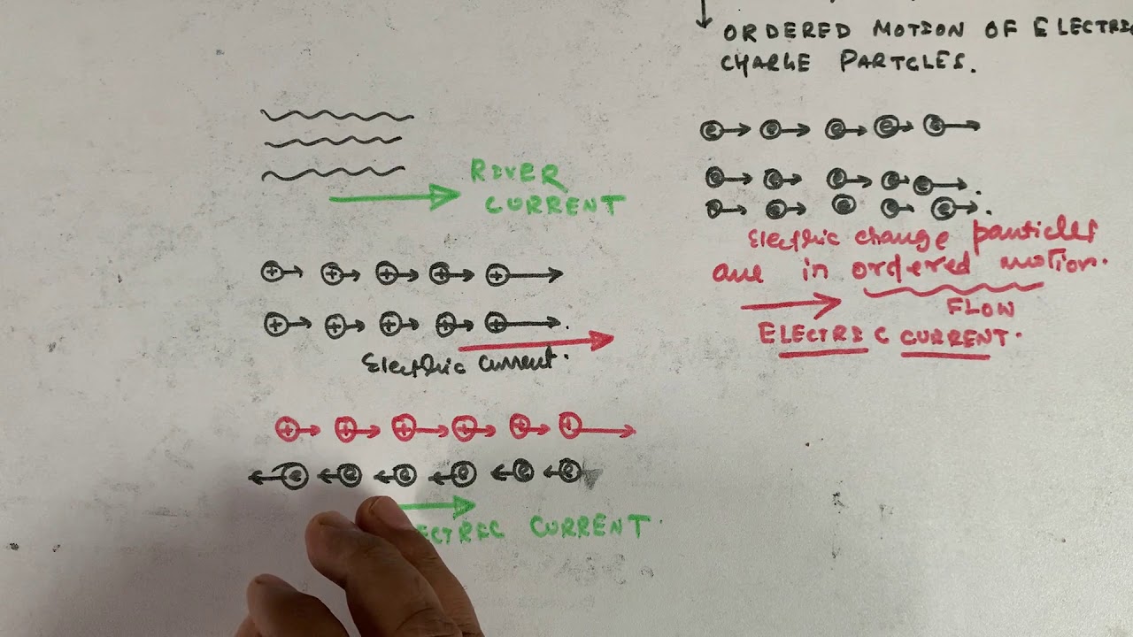
The fundamental definition of electric current as the flow of electric charge.
The distinction between conductors, insulators, and semiconductors in terms of electrical conductivity.
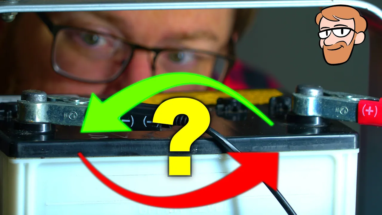
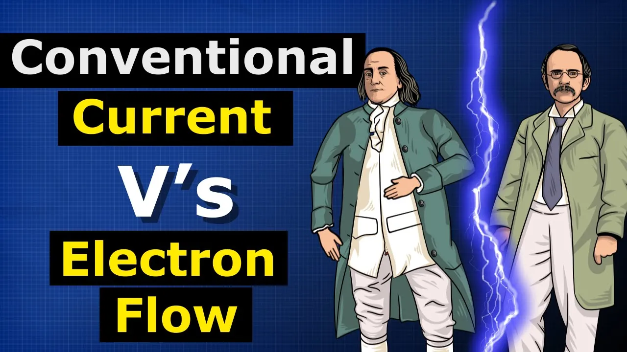
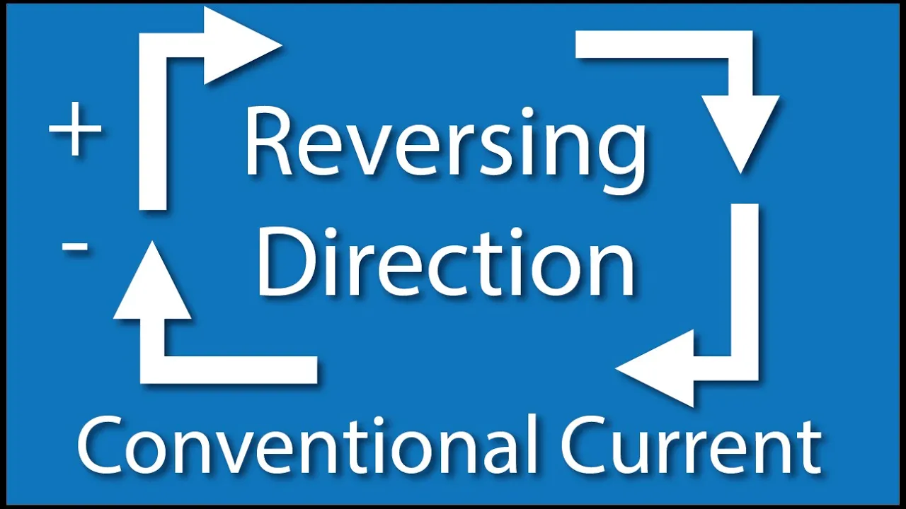
The concept of conventional current flow versus electron flow in basic electric circuits.
The process of doping semiconductors to create P-type (positive hole-rich) and N-type (negative electron-rich) materials.
The physics and behavior of P-N junctions, which form the basis of diodes and rectification.
The operation of transistors (such as BJTs and MOSFETs) as electronic switches and amplifiers.
Energy Band Theory, including the valence band, conduction band, and bandgap energy in solid-state physics.
1K views4likes6:12Original Release: 2023-01-09
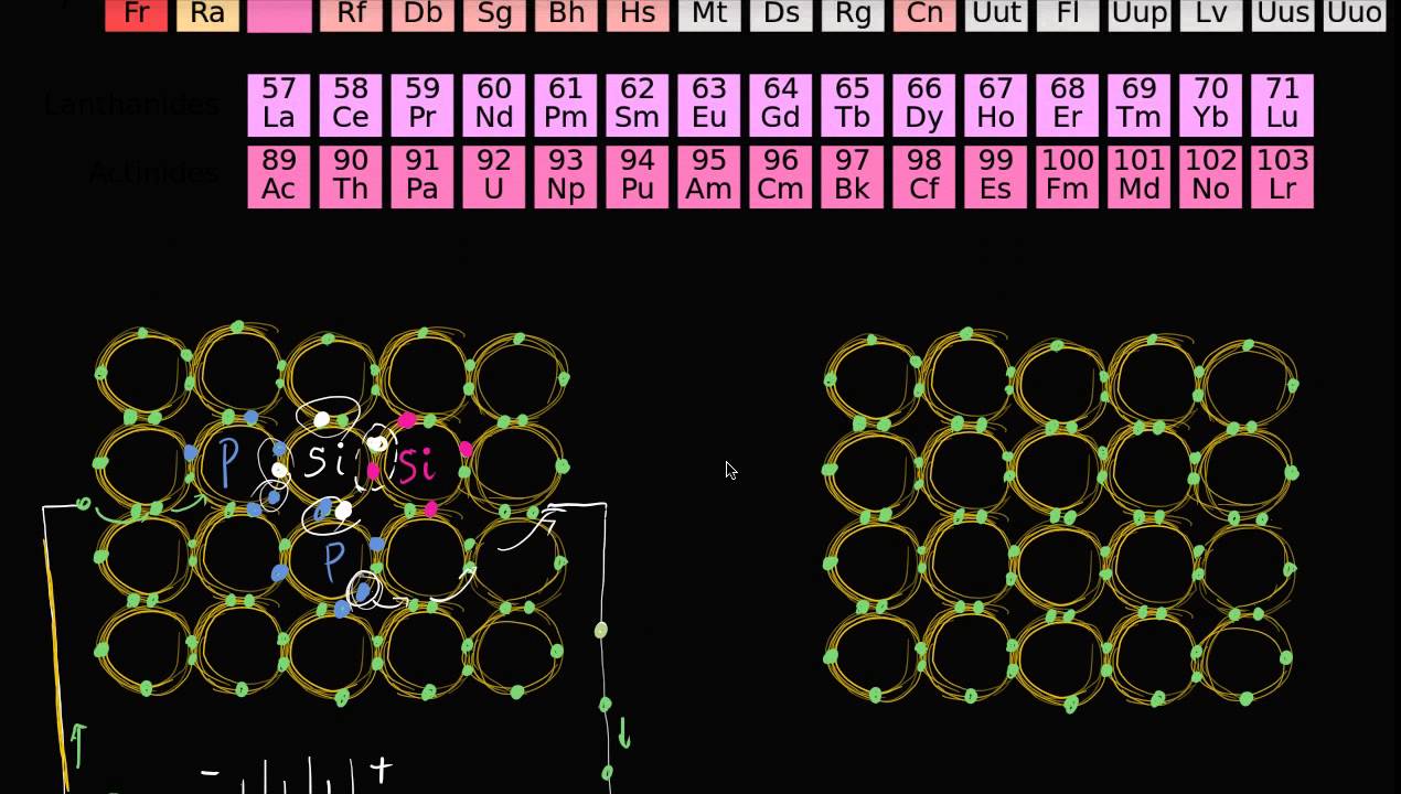
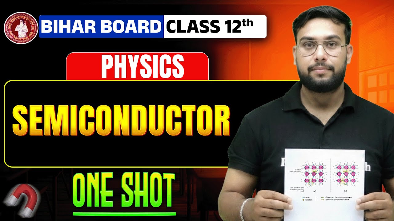
so before talking about the better way of making semiconductor we need to actually uh talk about something called host or the concept of holes okay so then we talked about a silicon crystal and we said that well if I heat this up I'm going to have these electrons are going to basically absorb some thermal energy and they're going to basically break away from their bonds right so when an electron actually leaves the bond it leaves a void behind it right we're going to call that void a hole this void is basically uh well a free space for an electron to come in so that the valence shell of this silicon atom is going to be completed right so we're going to call those voids uh holes and uh if you think about it let's say that I have this hole at t equal to T1 I have this hole at this location right few moments later at t equal to T2 this electron here um let me yeah so this electron breaks away and the electron actually come comes and basically fills up that previous hole now my hole is actually moved from here to here right and at t equal to T three the hole actually moves from here to there right so if you think about it in reality it's the electron that is moving from right to left but if you look at this from a like a visual perspective it's actually easier to see that the hole is actually moving from left to right right so this is actually so the hole is like the absence of electron it's not really a an object or like it's not something physical that you can actually uh touch it or like basically feel it or well not that the electron is but anyway you know what I mean so the the holes don't exist physically but they're actually pretty useful for us to actually express some sort of a current to see how sometimes to to actually explain how the current is actually generated or in which direction the current is moving um expressing it in terms of holes has actually become um quite interesting and it it it actually makes our lives much easier uh you will see that in the future slides of this lecture this week's lecture [Music] um uh in more details Okay so one thing we will notice later is that the holes are actually moving if uh when we when people measure the movement of holes the holes are actually moving slower than electrons and you might think that well didn't you just said that electrons and holes movement are pretty much the same thing it's just different perspective uh yes and no so electrons could actually move freely without getting trapped by these holes right so we have two different mechanisms for electron movement so when an electron is basically is broken away from a bond it can actually move freely across the crystal so if you apply a voltage across the crystal that voltage is going to cause an electric field and that electric field is going to move the electron from one uh from one end to the other end right and if the electron is not trapped into any of these holes it's just going to move freely and at the different speed right but then with holes it only happens like basically they only move when an electron is actually trapped and then released and then then trapped and then released right so they are slower because electrons the holes only move or the hose movement is based on a trap and release mechanism so you can even think about it that way that like basically holes are those electrons that get trapped and then they they get released and then trapped again and then released again and trapped again and then we have the different category of electrons that just that they're just moving right so uh they don't get trapped so like they can actually move freely they're gonna move it they're gonna move much faster than those electrons that get trapped and released that's why holes are actually uh are slower in general uh than electrons right the other question that we might have is that well how many holes do I have inside the silicon crystal well if you think about it we only have holes when we have an electron that is broken away right so the number of holes or the density of holes is going to be equal to the density of electrons so if I uh show the density of holes as p and density of electrons is n and by electrons I mean the free electrons right they're going to be equal to each other equal to ni right so for Pure silicon crystal um I can say that P is equal to n is equal to ni right another thing that they can say from this equation which is very simple kind of a deduction mathematically but very important in terms of semiconductor physics is that n times p is going to be equal to ni squared right so we're going to see that well mathematically this is very simple like n is equal to P is equal to ni so n times B of course it's ni squared right but we're going to see that not only this is correct for Pure silicon crystals we're going to see later that even in extrinsic semiconductors uh meaning that for semiconductors that are made of different types of elements different types of material this equation is still valid and it's going to actually help us a lot in terms of calculating the density of holes and density of electrons
Up Next

10:36
The PN Junction Explained: How Diodes Work | Semiconductor Physics
@fmgomezcampos
1.2M views•2013-05-04

12:53
21cm Hyperfine Transition in Neutral Hydrogen: Radio Astronomy Basics
@AaronRobertParsons
12.4K views•2011-10-13

32:32
NMR Spin Physics I: Zeeman Effect, Resonance Condition & Larmor Frequency
@nptel-indianinstituteofsci8064
2.3K views•2024-01-17

27:14
Entropy and the Second Law of Thermodynamics Explained
@veritasium
27.5M views•2023-07-01
Related Study Plans & Knowledge Roadmaps
Structured learning paths in Physics
physics
Nuclear Physics (Decay, Fission & Reactors)
01Atomic Structure and the Binding Force
02Radioactive Decay and Half-Life
03Nuclear Fission Mechanics and Chain Reactions
+ 2 more learning modules
12h5 modules
Explore Roadmap
physics
Soft Matter (Polymers, Colloids & Rheology)
01Foundations of Soft Matter & Thermal Forces
02Polymer Physics and Macromolecules
03Colloids, Surfactants, and Self-Assembly
+ 2 more learning modules
38h5 modules
Explore Roadmap
physics
Analytical Mechanics: Lagrangian & Hamiltonian
01Mathematical Foundations: Calculus of Variations
02From Newtonian Mechanics to Constraint Dynamics
03The Principle of Least Action & Lagrangian Mechanics
+ 3 more learning modules
28h6 modules
Explore Roadmap
physics
General Relativity (Spacetime & Cosmology)
01Foundations of Relativity: Special Relativity
02The Geometry of Spacetime: Equivalence Principle & Curvature
03Einstein's Field Equations: The Mathematics of Gravity
+ 2 more learning modules
55h5 modules
Explore Roadmap