





![[25년 2회 전기산업기사 CBT 복원] 회로이론](https://i.ytimg.com/vi/jSbO2GSS3W8/maxresdefault.jpg)



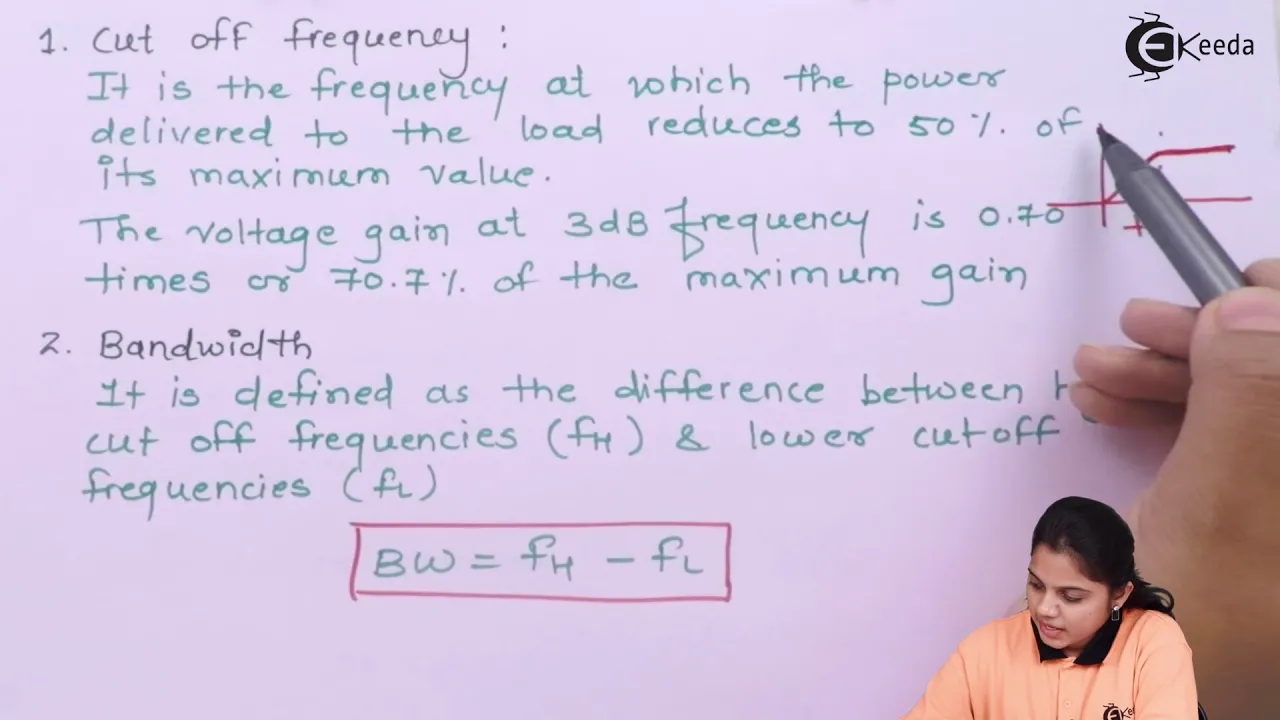
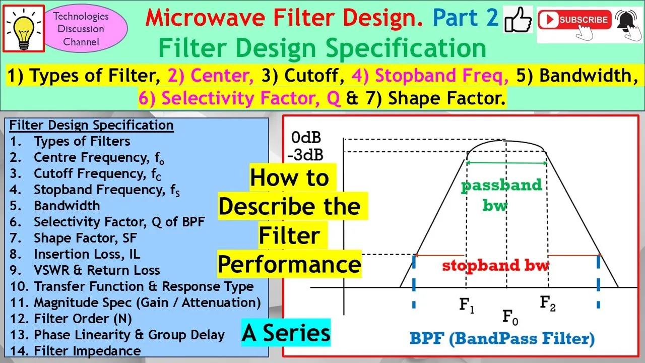








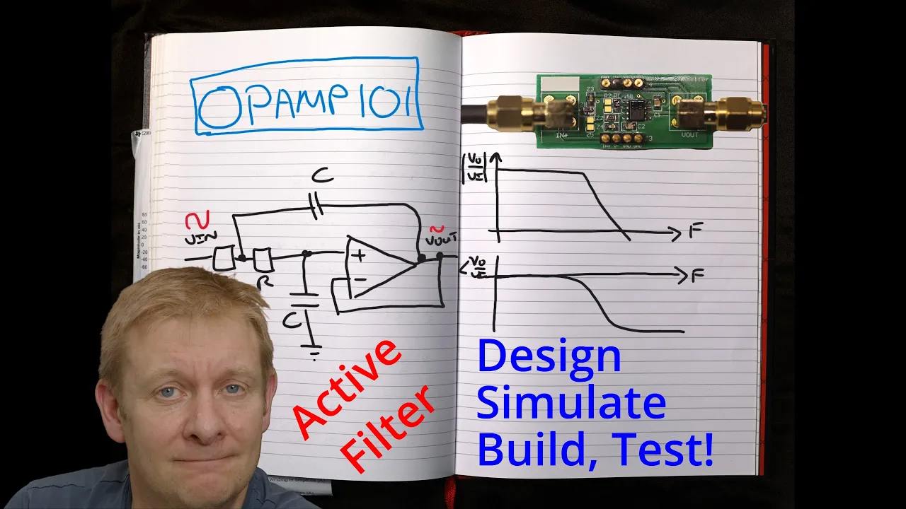






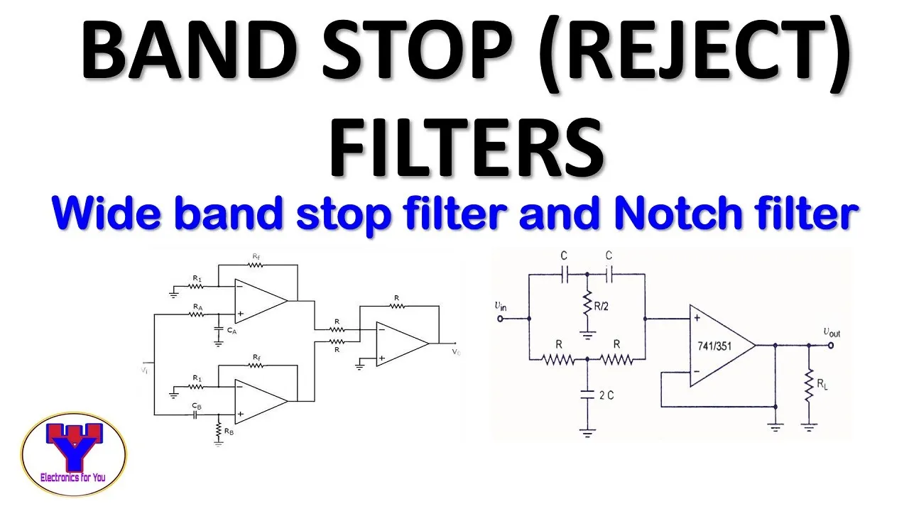

This lecture covers the analysis and design of second-order active KRC band pass and notch filters using operational amplifiers. For the band pass filter, the resonant frequency is derived as f₀ = √(2)/(2πRC) and the quality factor as Q = √(2)/(4-K), where K = 1 + RA/RB. The design process involves selecting equal component values (R1=R2=R3=R, C1=C2=C) and calculating RA and RB based on desired specifications. For the notch filter (band reject filter), also called twin-T network, the notch frequency is f₀ = 1/(2πRC) and quality factor Q = 1/(4-2K). Both filter types are verified using LTspice simulations to ensure practical implementation accuracy.
Second Order KRC Band Pass & Notch Filter Design Using Opamp
Added:Fundamental operational amplifier (op-amp) theory, including inverting/non-inverting configurations and the concept of virtual ground.
Basic AC circuit analysis, s-domain (Laplace transform) representation of components, and transfer functions.
Fundamentals of first-order active filters and the interpretation of frequency response using Bode plots.
Core filter performance parameters, including center/cutoff frequency, quality factor (Q), and bandwidth.
Basic familiarity with schematic entry and AC sweep analysis in simulation tools like LTspice.
Design of higher-order active filters by cascading second-order stages using Butterworth, Chebyshev, or Bessel approximations.
Comparison of KRC (Sallen-Key) topologies with alternative active architectures like Multiple Feedback (MFB) and State-Variable (Biquad) filters.
Analysis of non-ideal op-amp limitations, such as finite Gain-Bandwidth Product (GBP) and slew rate, on filter behavior at high frequencies.
Sensitivity analysis of active filters to evaluate how component tolerances affect the filter's Q-factor and center frequency.
Practical applications of notch filters in noise rejection, such as removing 50/60 Hz power-line hum in biomedical (ECG) and audio signal processing.
1.1K views9likes36:53Original Release: 2020-12-06
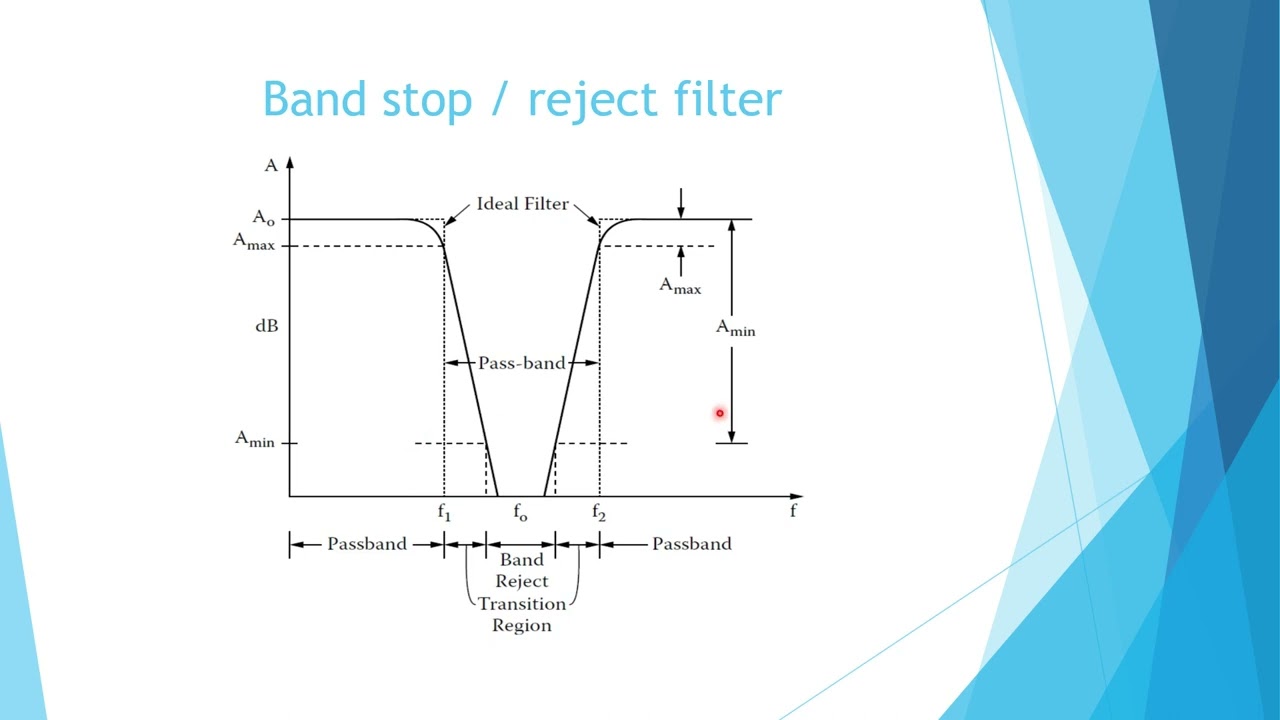
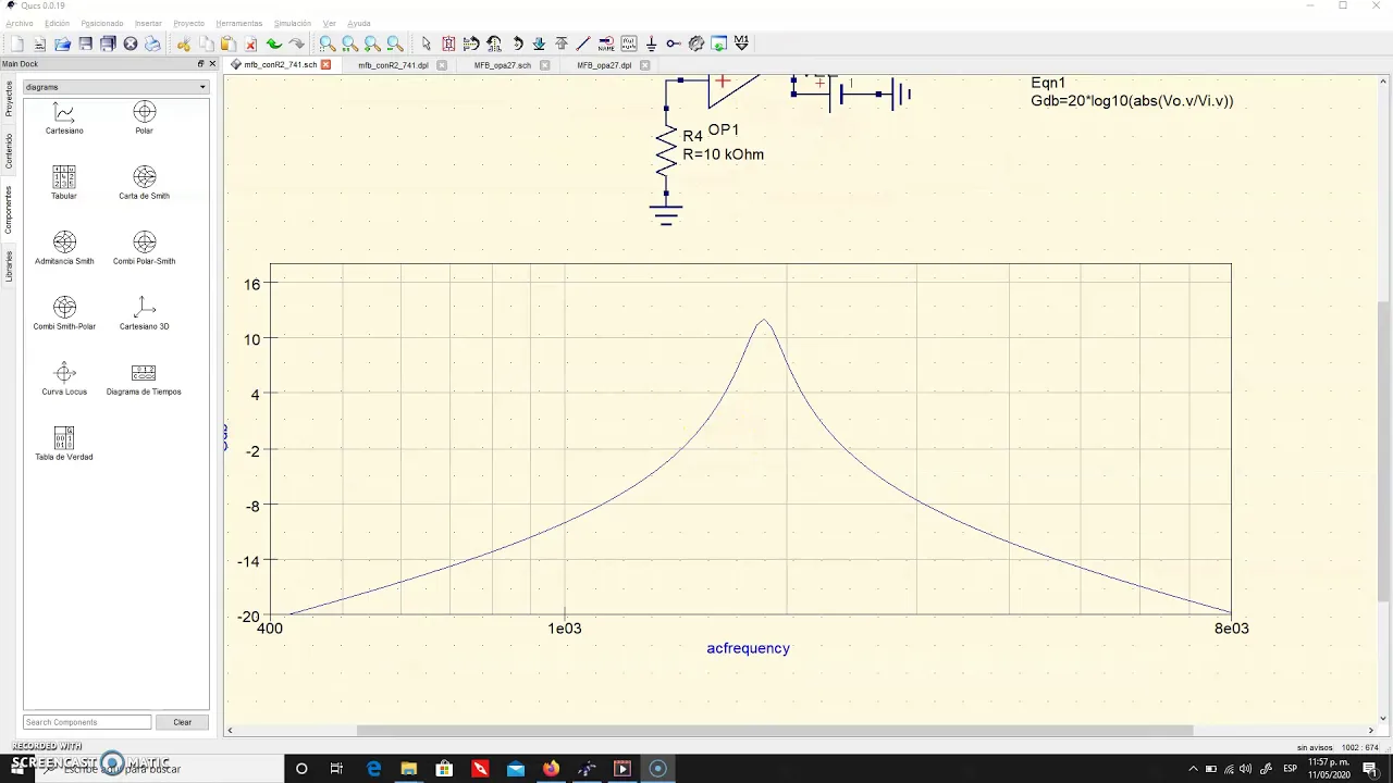
okay hello everyone welcome to LCD lecture 41g there are four topics which we will which we will be discussing today first one is second order active KC band pass filter we'll analyze the circuit see its frequency response and we'll verify some values with ltpy simulation then we'll see the generalized transfer function from there we'll derive the cut off frequency F not and the quality factor for the same then we will see one more design of uh you know the second order active KC P pass filter and next we'll go to the band reject KC filter or a notch filter we'll analyze the circuit and its operation and also build up its frequency response lastly we will design a notch filter which will include the design steps as well as the LT spice verification of the design values okay so let us begin with the lecture so let me put this in a full screen mode okay yeah so this is my second order band pass filter the circuit is exactly more or less similar only thing is that the RNC components are are uh inversely placed over here so in case of your It's a combination of uh you know the low pass and high pass response basically okay so here we have only additional AR element which is present from the output to this terminal okay and here the first capacitor is grounded and the second R2 resistor is also grounded so that's the difference between the earlier filters which we have discussed that is low pass and high pass it also consisting of two RC elements but here additionally there is a R3 resistor which is present over here okay so here we have RB as usual so this is again the opam non-inverting configuration input is been applied to the resistor R1 C1 combination followed by R2 C2 which is connected to the noninverting input terminal of the opam and R3 is the additional registor which is necessary for a band pass KC filter okay so the observations are the about circuit consist of an RC stage followed by a CR stage to uh get a band pass response and a gain block to provide a positive feedback via R3 register okay thises feedback is designed uh to to improve the response near Omega by Omega not which is equal to one okay so this is my frequency response for my band pass second order band pass filter as you can see very clearly the band of frequencies between Omega L and Omega H are passed whereas all other frequencies that is frequencies below Omega L and the frequencies above Omega H are rejected where H BP over here is my resonant gain or my uh you can say the band pass gain and Omega not is the peak order resonant frequency okay so this point is clear so all the frequencies below Omega L and above Omega are rejected at the rate of 20 DB per decade and my bandwidth of this uh band pass filter is given by Omega H minus Omega L now let us see that derivation for this so uh actually I will just be describing I'll will not be deriving entire steps I'll be just keeping it static for 5 seconds you can dot it down in your notebook you can pause the video and you can try it out yourself because the more important thing that is a design is focus over here so for the derivation for f not and and quality Factor we will use admittances so your various capacitors and registers are used as admittances and your we can apply the KCl and uh KCl at V1 and vs2 and then we'll find the relation between V 0 and V1 okay here the output voltage is given by V out is equal to 1 + ra upon RB into V2 because it the V2 is the input to the Inver non-inverting terminal so this amplifier this circuit is waving as a non-inverting amplifier basically in terms of V2 being the input so here K is 1 + ra upon RB so V 0 will be K into V2 now we have to determine the relation between v0 and v in so for that we apply KCl at V1 so you can have a look at it okay I'm not describing it so you can have a look at the diagram as well as this so I will describe only the first step rest of the steps we can follow it up so KCl at V1 gives us all our outgoing currents so V1 minus V into y1 V1 minus V2 into Y2 V1 into Y3 + V1 - V 0 into y5 so you get this used expression over here we substitute uh instead of V2 uh in terms of v0 so we get equation number one in equation number one we also have V1 present so next step we have to apply the KCl at V2 so KCl at V2 gives us V2 - V1 into Y2 then V2 into Y2 y4 is equal to Z so that's what we get V2 - V1 into Y2 V + V2 y4 is equal to Z so from here we get the relation of V1 in terms of V 0 we substitute that in equation number one okay and we rearrange this term such that the transfer function will only contain v 0 and V so h of s that is equation number three is my transfer function generalized transfer function in terms of admittances now for a band pass filter we substitute these values in terms of component so y1 will be 1 upon R1 Y2 will be S C2 Y3 will be SC C1 y4 will be 1 upon R2 and y5 will be 1 upon R3 you can check it out cross check these values with the actual diagram so with this diagram as well as this diagram you can compare it you will get those numbers we will get those results and in this if we if we consider the equal component design to simplify the mathematics so what we will do is we substitute uh R1 = to R2 = to r3al to R and C1 equal to C2 = to C so then your admittances y1 y4 and y5 will be same equal to 1 upon R and Y2 and Y3 will also be same which will be S into uh C so if you substitute that in the general expression given in equation number three you will get the following result okay so H ofs will be this huge term so here we'll divide and multiply by R square finally after after slight multiply after slight uh simplification you will get H of s as K by2 into SRC / s² r² c² ID 2 plus SRC into 4 - k / 2 + 1 so we substitute s = to G Omega so that we find the transfer function in frequency domain so h of G Omega will be K by2 into G Omega RC divided by 1 - Omega s r² c² / 2 + J Omega r c into to 4 - k / 2 so this is our equation number four so this equation number four we compare with the standard form of band pass filter let us check the standard form so these are standard second order responses uh let us check the band pass response this is high pass respon this is band pass response as you can see over here we have in the expression hobp so hobp is a resonant gain and uh over here right so h o BP into J Omega upon Omega into Q divided by 1 - Omega upon Omega squ plus J Omega upon Omega divided Q so that's the standard form of band pass filter okay the standard form of all band pass second order band pass filter is H of G Omega so this is your h of G Omega which is given by so hence we write compare this uh equation number four which we got over here equation number four if it is compared with equation number five we can get this terms 1 upon Omega Square so let me just reduce it okay so over here 1 upon Omega Square will be given by R sare c² by 2 so Omega not will be Omega Square will be 2 upon RC squ so Omega will be square < TK of 2 divided RC so F will be square otk of 2 divided by 2i RC so this is the resonant or the center frequency of the second order band path filter similarly if you do the further comparison you will get 1 upon Omega 0 Q will be equal to rc into 4 minus K divided two so let us compare this yeah this term if you compare G Omega is present so 1 upon Omega Q will be equal to rc into 4 - k / 2 that's what we get over here so over here if you write Q in terms of Omega not so it will be two if you simplify this further you will get Q is equal to 2 * divided RC into 4 - K into Omega and Omega is sare root of 2 into RC so over here we get the quality factor for a and pass filter which is given by the equation square root of 2 ID 4 - K now one more term is there so we need to determine the value of you know HP so from the standard form HP into uh J Omega upon Omega Q will be equal to K by2 J Omega RC so that's the value which we are getting so H VP divided Omega into Q will be equal to K by2 RC so we substitute the values of Omega and Q over here and after simplification your passband gain or the resonant gain the band pass filter is given by HP will be equal to k / 4 minus K okay so for a band pass filter your quality factor is given by Omega upon bandwidth so your quality Factor over here is given by F divided by bandd which is Omega H minus Omega now let let us see the design now so we'll design a second order band pass filter with a cut off frequency of 1 khz and a bandwidth of 100 HZ okay and also find the resonant gain so this is the design statement given we will adopt a equal component approach so in the equal component design approach R1 will be equal to R2 will be equal to R and C1 will be equal to C2 will be equal to C so over here and ra and RV values are also to be found out so all the unknown values of resistors and capacitors we have to find in this design so the formulas are as given as follows h of VP is K upon 4 minus k Omega not is < tk2 / RC Q is < tk2 / 4 - K okay so now uh let us go proceed further so for a band pass filter the frequency is cut of frequency resurant frequency is < tk2 ided 2 pi RC which is equal to 1 Kil Herz given so let us consider the value of CS 10 nanar so C1 will be equal to C2 will be equal to 10 nanopar then we can find the value of r as run2 divided 2 pi f f is given as 1K and C is 10 nano so you'll get a number close to 22.5 you can take a standard value 24 kilms standard now we know the quality factor is given by the formula f divided by bandwidth here the bandwidth is given as 100 Hertz and F not is 1K so q q will be 1 khz divided by 100 Herz which will be 10 so once Q is 10 we can easily find reverse calculate K so K will be given by Q is given by < tk2 * < tk2 / 4 - K which is equal to 10 so K will be given by 4- < tk2 upon Q so you substitute over here you'll get the value of k k as 3.85 8 so D are the values of K which you get so K over here is 3.85 so K will be equal to 1 plus ra upon RB so ra upon RB will be 2.85 so that means ra will be 2.85 * RB so let the value of RB as 10K so value of RA will be 28.58 kils so we can substitute the standard value close to around 27 Kil standard value okay now the last thing is we need to also find the resident gain so the passband gain so resident gain is given by K upon 4 minus k k is 3.85 which we have evaluated over here yeah so the passband gain will be k ided 4 minus K that will come out to be 27.2 that number will be 27.2 okay so here is my design circuit with all the values R3 R A RB C2 C1 R1 R2 okay so this is designed for a b band pass second order band pass filter for a cut of what a resonant frequency of 1 khz and bandwidth of 100 HZ okay so let us check out that this design in LT spice now okay let me open the LD spice window and let me close this and open the band pass filter design okay band pass filter equal component design okay here is the circuit so we have taken the exact value of resistors over here [Music] okay so here we have it ra was 28.58 KS our V is 10 KMS then uh the value of R was 22.5 KS and all the RS R1 R2 and R3 and the value of all the capacitors were 10 10 nanofarad so here it is so I taken the exact values because we have the flexibility in LT spice to do so so now let's check out the frequency response so this is my circuit I have built up in LT spice so you all can also similarly build up and check the response I have used opam op07 so we'll go to simulate click on run and let's check the output yeah so here we have it so here I have my band pass response right second order band pass response as we have discussed in the theory it will exactly look like this let me show it to you yeah here it is see this is what we have discussed and this is what we are getting over here exactly the same now let's check everything over here one by one let us go back to the design values okay so D set the design values so first of all the uh cut off frequency we'll check the resonant frequency is designed for around uh how much is the value of the cut of frequency 1 khz Okay so it's designed for 1 khz and uh let's substitute the values as per the design so let's say I have 24K I think it is 27k over here yeah let us check it out as let us substitute as 27k standard values and check here it will be 24K here also it will be 24K and finally here also 24K okay now let's check out with the design we have taken the standard value of resistance and I think it won't matter that much let me just undo all the values so what I was trying to do was I was checking whether the cut of frequency range is properly coming or no so over here the highest frequency will be my resonant gain so at khz I'm getting over here so it's slly less but it's nevertheless let's check that number once okay it's definitely behaving as a band pass filter as you can see very clearly some frequencies are getting uh you know as you can see it's a range of frequencies and the range will be 100 HZ basically so the highest value over here which we are getting 1K we are getting over here you know one kilo Kilz we are getting over but we should get that at the maximum value that is over here that's fine that not a problem not a problem so we can check the value now okay so the highest value of the h BP will be 27.2 so we can take 20 log to the base 10 20 7.28 okay so that's fine that we will check it later but uh the nature of the response is quite same maybe the cut off frequency the the the resurant frequency is not coming at the peak it's coming little bit aside so that's fine and we have to go 3db down and check out the values for the for the for the range of bandwidth okay so it is providing a it should provide a cut off frequency of 1 khz and a band we of 100 HZ but I think it's providing a bandwidth slightly different than that that's okay but the nature of the response is absolutely correct fine so here was the the frequency response of a KC band pass filter and this was the design equal component design equal component design will always give some shift in the you know slight shift in the frequency because there are so many resistors and capacitors connected so they're bound to happen some frequency change so 1 khz is coming over here okay at around minus 3 DB uh you are getting around 1 Point 01 okay highest value over here is uh 1.3 so if you come 3db down you will get this range of frequencies it's fine I think the nature of the response is correct we should not bother too much about the cut off frequency okay now let's go to the next topic so the next topic is the ban reject KC filter or it is also called as active twin filter or Notch filter so Notch filters are used when it is necessary to remove a signal single frequency from a signal okay so this is our band twint Network or a your opam is connected in a non-inverting mode basically and uh it it has a twint so you can see c c and this R by2 forms a t Network and this r r and 2C forms the inverted T Network so that's why it is called as a twin t Network and the positive feedback is given via this part and a negative feedback is given via this part so opam is working in the non-inverting mode with input as v+ okay and the gain as 1 plus ra upon RB that's that's definite so how thises 20 circuit works so the opam is in the uh let me reduce this slightly prop is in a non-inverting mode that's why output is given by 1 + ra upon RB into v+ which will be K * v+ so output will be K * v+ actually now this is the frequency response of a notch filter so as you can see it's removing only one frequency whereas the bandw is quite low so it has one stop band and two start uh two passbands so h n is my stop band gain uh basically and this is my Notch frequency so you will remove only one frequency from all the frequencies okay so this is the typical response frequency response of a notch filter and this F is called as the notch frequency okay so how does the working goes I think I have to open one more PDF of this let me do that quickly okay I'll paste one PDF over here and I have to open it because uh the circuit diagram is required for explanation will be required actually okay I can place this over here and second PDF I will open it over here okay that's fine now so we have got both the PDFs same PDFs only but for explanation I have to keep one PDF open for the diagram purpose okay I'll quickly go to the 20 Network okay so this is my circuit diagram so we'll concentrate on this circuit diagram and limit answers to this okay and on the left hand side I'll describe the theory behind it okay so let's see the working so the ciruit will consist of twin t Network and a gain block to provide the positive feedback via the top capacitance 2C so the TNT Network provides alternate forward paths through which the V can reach the amplifier input okay so uh we have a low frequency part given by RR and we have a high frequency part given by CC okay so let's consider this at low frequencies the reactance offered by the capacitance is high cor because XC reactant and the frequency are inversely proportional if the frequency is very very low the reactant is very very high so so the capacitors will behave as a open circuit so all the capacitors will behave as a open circuit but input will reach the amplifier via RNR by via this network RNR because resistor have no effect on the frequency now at higher frequencies the reactance offered by the capacitances becomes very low capacitors behaves as a short circuit so the input reaches the amplifier now we know that if you have a resistor and a short circuit the short circuit part will be preferred because the current always refers the least resistance part so at a higher frequency uh this capacitors will behave as a short circuit and the input signal will reach to the input terminal of your op Pam via this Capac two capacitors C and C at intermitted frequencies uh maybe at some particular intermediate frequency the two parts provide opposite face angle okay so it might happen that this part and this part face angle will cancel out so indicating the tendency that the two forward signals cancel out each other at the amplifier input so in that particular case no amplifier input will reach the input terminal of your opam okay so that means it will reject the not frequency that is the intermediate frequency so we does anticipate a not response as observed in the frequency response of Notch filter so that's why we get this kind of a notch response wherein this response will indicate that it will remove the notch frequency from the circuit okay so if we analyze uh AC analysis of the circuit gives the transfer function in the following form we have not derived it one can derive on the similar manner on the lines of low high pass and band pass response so here I'm directly writing the result so this is the standard not response equation I'll show it to you Notch filter so here we have a notch response H into 1 - Omega upon Omega s divided 1 - Omega upon Omega Square plus J Omega upon Omega into Q so that's the equations which we are getting and while deriving when you derive it you will get the values of h n as K which is the actually it's a stop band gain we can call ah it is a passband gain sorry and Omega not is the not frequency which is 1 upon RC Q is given by 1 upon 4 minus 2 Q or 2 k q is given by 1 / 4 - 2K where F not will be 1 upon 2 pi RC over here the K value is 1 + r upon RB and also the quality factor is also given by the formula f upon bandwidth so from the frequency response it is clear that now where is the frequency response over here yeah here so from the frequency response it is clear that uh that uh the circuit will reject the frequency around uh FAL to FN basically or Omega equal to Omega not with a maximum atation okay whereas it will pass all of the frequencies with the maximum passband gain so that is very very clear okay so let's go to the final design for for this online session online lecture so design a not filter having FN as 60 htz and a bandwidth of 5 Herz okay so the very first thing is the quality factors so quality factor is given by F not divided by bandwidth so F not is basically a not frequency over here it is 60 divided by bandw is five so quality factor is 12 now F not is also given by 1 upon 2i RC that is 60 HZ so from here let let us say that the value of C is 100 narad so 2 C will be 200 narad okay so we can calculate the value of R it comes out to be 26.5 26 KS we can take the nearby standard as 27 kils so the value of Q is given formula of Q is given by 1 upon 4 minus 2K so we can find the value of K from here so over here if we find the value of K that will be 4 minus I think uh let us check it out first so 2K will be equal to yeah so 2K will be 4 - 2K will be equal to 1 upon Q actually this should be the whole should be divided by two actually but that's fine I think there is some mistake in this step uh Q if I substitute the value let me put the values in the calculator and check so Q is around 12 so Q let me put the values in the calculator Q is around 12 divided by 1 / 4 - 2 into let me substitute this value now 12 is equal to so okay so uh 4 minus 2K let me open The annotation so let let just check it out now so it will be 4 minus 2 K will be equal to 1 divided by Q correct so what will be K so actually I can write it as 2K will be equal to 4 minus 1 ided Q okay yeah I am right so K will be equal to this term entire term whatever I'm getting divided by two okay so K will be equal to half of 4 minus 1 upon Q so that's the value of Q actually okay so that's the correct answer I think I made a mistake over here so we can correct it so it will be 4 minus 1 / okay 1 / 12 fine divided by two so your value of uh [Music] of K is coming out to be let me just write it over here so actually it is 40 just a second 4 divided by 1 uh 4 - 1 / 12 so that is divided by two yeah okay okay okay the formula is wrong but the calculations are correct okay so over here this is actually taken as into half only I have just that it is not written it over here so actually this is multiplied by half only so this is multiplied by.5 okay this is multiplied by 0.5 so if you put it in a calculator uh this will be 2 - 1 / 6 that will [Music] be okay so four let me just check it once more 4 - 1 / 12 and uh that multiplied by.5 yeah the answer answer is correct yeah answer is correct but only your half sign is missing so please add that half sign over here in this okay now let me close The annotation okay so K will be 1 + ra upon RB 47 upon 24 which will be equal to R RB is 23 divided 24 so let the value of RA will be 10 KS similarly the ra sorry RB will be 10 Kil so ra will come out to be 9.53 KS so let's consider the nearby value of 9.5 K standard I think 9.5 KS is not a standard you can consider 9.1 KS as a standard value so nevertheless we'll substitute the same value in LT spice actually so your design circuit will look like this okay now let's quickly simulate this because this was R and R all RS were same and this was R by2 so this will be half of this 27 kilms and this will be twice C so this will be 200 nanopar okay so let's simulate this Notch filter 60 HZ Notch filter okay let me close this and let me open a circuit for a notch filter band reject KC filter basically okay so this is the response over here let me just check the value so this is the 20 Network 2 see this will be 100 100 narad this will be 200 nanofarad this will be around 27 I told you have taken the exact values not the standard values and over here we have it as ra and RB 9.53 and 10K okay so the design is absolutely correct now let's check this value whether it's give a not response or no yeah yeah so it's giving perfectly well good results over here as as you can see clearly see it's rejecting a unique frequency now let's check what is that frequency it should be close to 60 HZ so let me magnify this a little okay so if I place this down I'm getting 63 htz okay instead of 60 htz I'm getting the notch frequency at 63 HZ that's absolutely fine and uh this is how we will get a proper you know uh response not response will be 63.9 Hertz and we have designed it for 60 HZ so that's quite close even if you tune your components a little more closer you will get a more tighter control over the frequency okay and uh the pass band game well one can check that also so over here it was around uh 47 divided by 24 20 log of that okay so somewhere close to Let's see 5.83 we were getting it but uh here the pass band gain will be 5.8 DB so instead of 5.83 we are getting 5.8 DB as the F band gain and with a notch frequency of 6309 Hertz okay and if I come down by uh let's say 5.88 DB right so I have to come down to how much uh 2.8 [Music] DB sorry I have to come 3db down right so that's absolutely fine we can come 70.7% of the highest value down also so that will give me around uh yeah so your not frequency will be close to 63 HZ and the passband gain is 5.8 DB so that's enough to calculate this uh you know evaluate this band reject filter now band reject filter is practically used in biomedical applications to remove the 50 HZ or a 60 HZ noise signal okay so designing such a filter giving such a response is also very very important and these are analog filters so using your registor active elements as opam you can build this uh Notch filters very very easily with the correct values of R and C in the circuit so this is also called as a TN Network as you can see active 20 or band reject KC filter it has three names band reject KC filter active 20 Network or Notch filter okay so this is how we see this uh topic and we have completed we have come to an end and we have completed the notch frequency uh Notch filter also and these were the results which we have got okay so we got 63 HZ as the notch frequency and the pass band gain was 5.8 DB okay so this is how we get the ban reject filter or the notch filter frequency response I think that's it uh for today's online session next time we'll start with a multiple feedback uh you know filters low pass filters let's say okay so that's it for today uh thank you for your time until we meet again next time so till then have a good day and thank you
Up Next
10:24
DIY Electrocardiography Circuit Using Op-Amps | ECG Amplifier Design
@EngineerSarah
26.3K views•2023-11-21
30:32
Ultrasonic Transducers: Resonant Frequency Measurement and Horn Design
@imajeenyus42
229.9K views•2017-02-22
54:16
Polymer Environmental Degradation: Mechanisms & Stabilization
@iit
1.8K views•2012-07-10
33:39
How a Student's Question Saved a NYC Skyscraper from Collapse
@veritasium
22.8M views•2025-04-26
Related Study Plans & Knowledge Roadmaps
Structured learning paths in Engineering
engineering
Building Acoustic Levitators: Physics & Arduino
01The Physics of Sound and Standing Waves
02Piezoelectric Transducers and H-Bridge Drivers
03Arduino Programming: Generating 40 kHz Signals
+ 2 more learning modules
14h5 modules
Explore Roadmap
engineering
Building Peltier Cloud Chambers: Particle Tracks
01Cosmic Rays & Cloud Chamber Physics
02Thermoelectric Cooling (TEC) Fundamentals
03Custom Liquid-Cooling Loop Design
+ 2 more learning modules
18h5 modules
Explore Roadmap
engineering
Yagi-Uda Antennas: Modeling, Build & VNA Test
01Introduction to RF and Antenna Fundamentals
02Yagi-Uda Antenna Design Principles
03Antenna Modeling and Simulation in 4NEC2
+ 2 more learning modules
18h5 modules
Explore Roadmap
engineering
ECG Monitor Design: Op-Amps, Filters & Noise
01Electronics & Breadboard Basics
02Op-Amps and Instrumentation Amplifiers
03Bioelectricity and ECG Fundamentals
+ 2 more learning modules
18h5 modules
Explore Roadmap