A MEMS accelerometer measures acceleration by detecting changes in capacitance caused by the movement of a silicon microstructure (such as a center beam with comblike teeth) in response to external forces, where the ADXL05 model can measure ±5g acceleration along a single axis.
ADXL05 MEMS Accelerometer Teardown: 1996 Single-Axis IC Analysis
Added:Deep Dive
Basic principles of Micro-Electro-Mechanical Systems (MEMS), specifically how mechanical structures are integrated on a silicon substrate.

MEMS and NEMS devices
9.1K
MEMS (Micro Electromechanical Systems) are devices operating at 1-200 micrometer scales that convert electrical to mechanical energy and vice versa. They integrate micro sensors, actuators, microelectronics, and mechanical structures on silicon substrates through deposition, patterning, and etching processes. Key advantages include enhanced speed, reduced complexity, lower power consumption, smaller form factors, and superior system integration. The large surface-to-volume ratio at micro scales makes surface effects dominant, enabling unique mechanical behaviors through thin coatings. Applications span automotive (airbag accelerometers, tire pressure sensors), medical (blood pressure monitors), and consumer electronics (inkjet printers).
Click to watch →
Introduction to MEMS-Lecture 1
7.9K
MEMS (Micro Electro Mechanical Systems) integrates mechanical elements, sensors, actuators, and electronics on silicon substrates using micro fabrication. Key components include microelectronics (processing unit), micro sensors (environmental data receivers), micro actuators (device activators), and microstructures (integrated chip structures). Components range from below one micron to several hundred micrometers. Scaling laws distinguish size-dependent effects from material property effects; surface area relates to pressure, force, and heat transfer, while volume affects mass, weight, and thermal inertia. Three fundamental fabrication steps include deposition (physical vapor deposition, chemical vapor deposition, atomic layer deposition), patterning using lithography, and etching (wet etching with chemical solutions, dry etching with plasma/gas). Wafer bonding joins multiple wafers for stacked structures, requiring flat, smooth, and clean surfaces.
Click to watch →
MEMS (Micro-ElectroMechnical System) | Explain in Tamil | IC-Manufacturing Engineer must watch video
15.8K
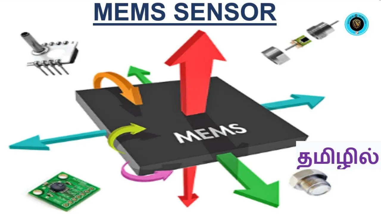
MEMS (Micro-Electro-Mechanical Systems) is a technology that integrates both active components (sensors and actuators) and passive components (electronic and mechanical systems) onto a single silicon substrate using advanced IC manufacturing techniques, enabling the fabrication of microscale devices such as sensors, transducers, gears, pumps, and switches that bridge the gap between analog physical parameters and digital electronic systems.
Click to watch →

Introduction to Micro Electro Mechanical Systems(MEMS) - Dr.M.Sangeetha
5.1K
Micro Electro Mechanical Systems (MEMS) are tiny machines (1-100 microns) that integrate electrical and mechanical components on a single chip, comprising sensors (to gather environmental information), microelectronics (to process data), actuators (to control the environment), and microstructures. MEMS applications span biomedical fields (intracranial pressure monitoring, drug delivery), automotive industries (crash sensors, airbag activation), consumer electronics (gyroscopes for mobile devices), and military systems (projectile guidance). The fabrication process involves silicon wafer preparation using Czochralski or float zone techniques, followed by micro-machining processes including surface micro-machining, bulk micro-machining, and lithography. Scaling laws dictate that reducing component size affects physical properties proportionally (e.g., volume reduces by 1000x when length is reduced by 10x).
Click to watch →

Micro Mechanical Systems (MEMS)
3.4K
Micro Mechanical Systems (MEMS) are miniaturized devices that integrate mechanical elements, sensors, actuators, and electronics on a common silicon substrate using microfabrication technology, enabling applications such as accelerometers, pressure sensors, microphones, and building management systems.
Click to watch →
Deep Dive
The physics of capacitive sensing, including how displacement changes the capacitance of a differential capacitor structure.

10 Lecture9
227
For a differential capacitive transducer with fixed plates separated by distance 2D and movable plate displaced by X, capacitances are C1 = εA/(D-X) and C2 = εA/(D+X). The differential output voltage is E2 - E1 = (V/2) × [X/(D² - X²)]. At the null position (X=0), output is zero. The sensitivity (change in output per unit displacement) is V/(2D²) at X=0. This mathematical relationship shows how displacement produces measurable electrical output, enabling precise position sensing applications.
Click to watch →
Capacitive Transducers: Principle of Working and Types
11.9K
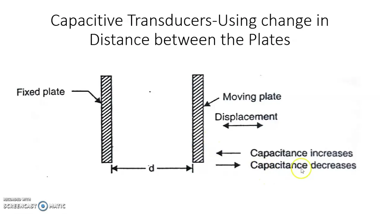
Capacitive displacement measurement using distance change exploits the inverse relationship C ∝ 1/D. As the movable plate approaches the fixed plate, reduced separation increases capacitance; moving away decreases it. The differential capacitor system employs a common central plate forming two capacitors. When displaced by X, one capacitor's distance becomes D+X while the other becomes D-X. Applying voltage yields output voltages E₁ and E₂, with their difference E₁-E₂ = E×X/D being directly proportional to displacement. This configuration provides high sensitivity and linear response for precision displacement measurements.
Click to watch →

Capacitive sensor, Theory, application and design
325.3K
Capacitive sensors detect objects by measuring capacitance changes across electrodes. Unlike the misconception that grounded fingers are required, sensors work through electromagnetic coupling. When an external conductor enters the electric field, it polarizes and allows more charge storage, increasing capacitance. Two plates are essential for detection, not one plate measuring against infinity. The system reaches equilibrium when charges balance attractive and repulsive forces, with capacitance defined as charge stored per volt.
Click to watch →

Numerical Examples
1.1K
Capacitive sensors operate on the principle that capacitance changes with physical parameters like distance, area, or dielectric material. In differential capacitive sensors with three plates (two outer plates separated by 100 mm and a movable intermediate plate), displacement causes unequal capacitance changes between the intermediate plate and each outer plate. When the intermediate plate deflects downward by x mm, the capacitance to the upper plate increases while the capacitance to the lower plate decreases. The differential voltage ΔV = V₁ - V₂ is calculated using voltage division principles: V₁ = [C₂/(C₁+C₂)] × V and V₂ = [C₁/(C₁+C₂)] × V. Substituting C₁ = ε₀A/(D+x) and C₂ = ε₀A/(D-x) yields ΔV = (x/D) × V. For D = 50 mm and x = 10 mm with V = 10 V, ΔV = 2 V.
Click to watch →

What is a Capacitive Transducer? | Operating Principle, Working, Types, Construction | KTU EC 307 S5
16.7K
The variable distance method measures displacement by changing the separation between fixed and movable plates. Since capacitance is inversely proportional to distance, moving the plate away decreases capacitance while moving it closer increases capacitance. The differential capacitor system improves measurement accuracy by using two capacitors sharing a common movable plate. When AC voltage is applied, the differential output voltage V_diff = E × (x/d) provides a linear relationship between displacement x and output signal. This configuration offers enhanced sensitivity and reduced errors compared to single-capacitor approaches, making it suitable for precision displacement measurements.
Click to watch →
Deep Dive
Fundamentals of semiconductor manufacturing, particularly photolithography, silicon maskworks, and integrated circuit (IC) packaging.
The Advanced Engineering Behind ASML's EUV Lithography Machines
18.2M
Microchip manufacturing begins with purifying silicon dioxide from sand into ultrapure silicon ingots, which are then sliced into wafers and polished. The core process involves photolithography: coating wafers with light-sensitive photoresist, exposing them through patterned masks, etching exposed areas, and depositing metals to create circuitry. This coat-expose-etch-deposit cycle repeats for 10-100 layers. The critical challenge is that as features shrink, diffraction effects become problematic, limiting how small patterns can be printed with conventional light sources.
Click to watch →
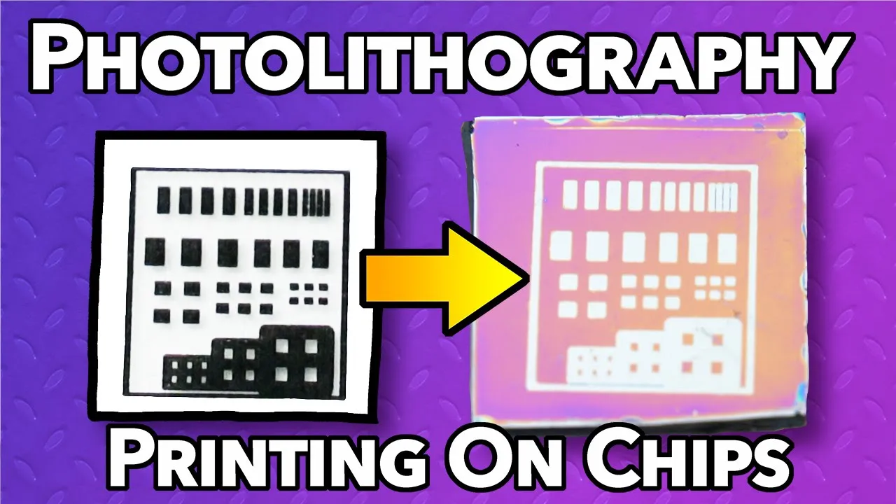
Photolithography on Silicon with PCB Chemicals
120.8K
Photolithography is the cornerstone technology enabling the miniaturization of semiconductors from individual transistors to billions on a single CPU. Developed by Jay Lathrop and James Null in 1952, this optical process uses light-sensitive chemicals called photoresist to transfer precise patterns onto semiconductor surfaces. The process involves applying photoresist, exposing it through a mask using light, developing to remove unexposed regions, and using the remaining pattern as a stencil for subsequent fabrication steps like etching or deposition. This technology enables the precision needed to create modern microprocessors that fit in our pockets while performing calculations far beyond human capability.
Click to watch →

Không có công nghệ này thì không có CPU bạn đang xài: photolithography là gì?
65.5K
Photolithography is the essential process for creating microscopic electronic circuits in semiconductor chips. The process involves coating a silicon wafer with light-sensitive photoresist, exposing it to UV light through a patterned mask, and developing the layer to reveal circuit patterns. Two main development methods exist: lift-off (removing photoresist from unexposed areas) and etching (removing both photoresist and metal in exposed areas). Modern chips require dozens of such patterning steps to create billions of transistors. The process demands extraordinary precision, with tolerances measured in nanometers, where even small errors can render chips non-functional.
Click to watch →

Как Производят и делают Процессоры? И из Чего? // #Полезные FiшКi
88.8K
Semiconductor manufacturing requires ISO class 3-4 clean rooms with strict air filtration and personnel protective gear. Design uses hardware description languages (VHDL, Verilog) and CAD systems. Photolithography transfers circuit patterns from masks to silicon wafers using light. Photoresist is light-sensitive material that becomes soluble or insoluble upon exposure. Photo masks are created using electron beam lithography with high-energy electron beams. Silicon substrates are made from monocrystalline silicon (99.999999999% purity) sliced into 300mm wafers. Steppers (ASML dominates 50%+ market) use DUV (193nm) or EUV (13.5nm) wavelengths. Three exposure methods exist: contact, proximity, and projection lithography.
Click to watch →

Leo Says Ep 66: Intel’s 5 Nodes in 4 years
29.6K
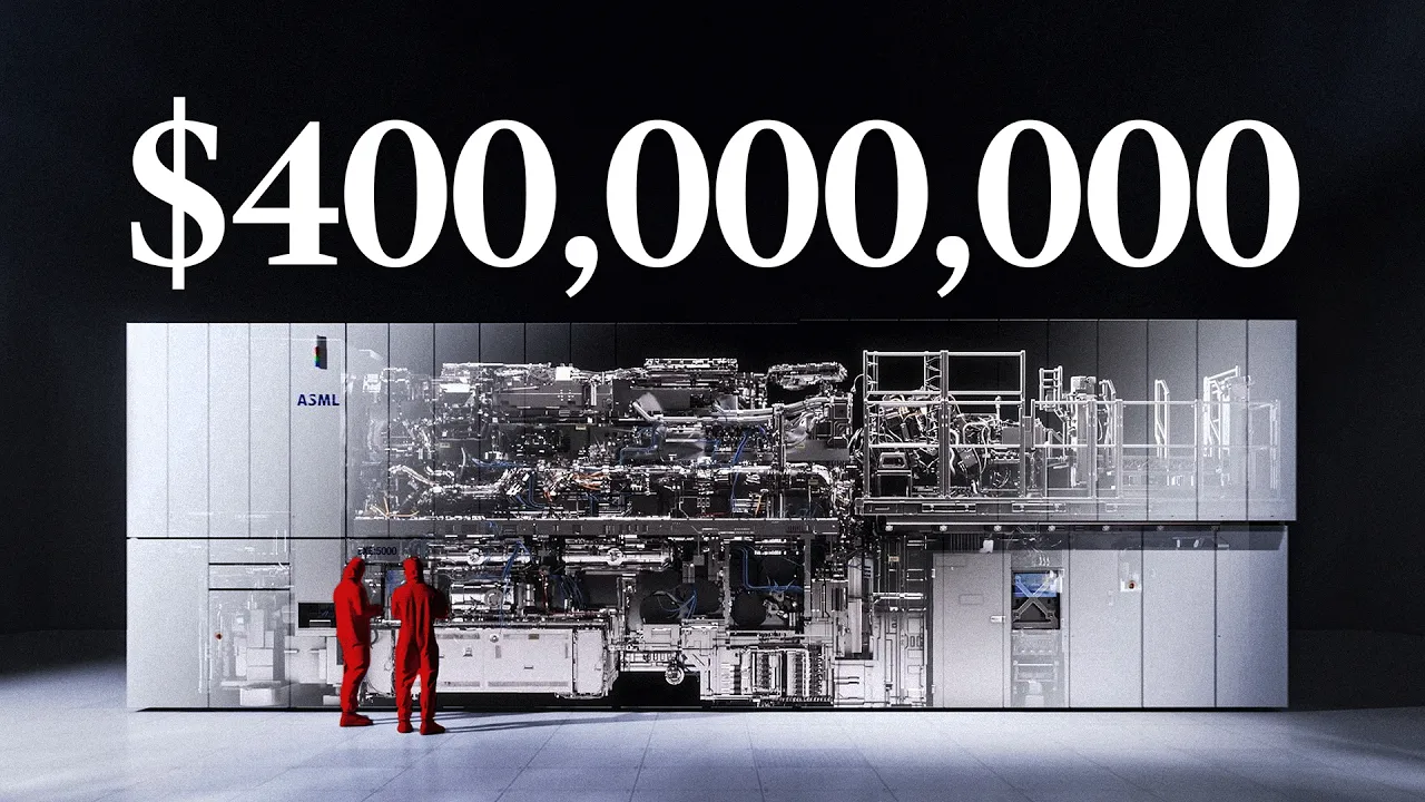
This section covers the foundational concepts of semiconductor manufacturing. The speaker explains that nanometer numbers indicate technology age (smaller = newer), but with 'FUD' (Fair Uncertainty Doubt) since adjacent numbers may not represent fundamentally different processes. Photolithography is compared to an overhead projector: light shines through a mask onto a silicon wafer with photo resists, then etching and cleaning build up processor layers. The key challenge is that light wavelength is too long for ideal precision at advanced nodes. DUV (Deep Ultraviolet) uses light too long for advanced work, while EUV (Extreme Ultraviolet) uses shorter wavelengths but costs $150-160 million per machine and is in short supply.
Click to watch →
Deep Dive
The Newtonian physics of mass-spring-damper systems and how acceleration translates to mechanical displacement.

Mass Spring Damper in SIMULINK | Modeling & Simulation Explained.
1K
The mass-spring-damper system is governed by Newton's second law: ΣF = ma. For this system, the external force F(t) is positive, while opposing forces are negative. The damping force equals the damping coefficient multiplied by velocity (c × v), and the spring force equals the spring constant multiplied by displacement (k × y). This yields the differential equation: m × y'' = F(t) - c × y' - k × y. Acceleration is obtained by integrating the acceleration equation, velocity by integrating acceleration, and position by integrating velocity. Key parameters include mass (m = 1 kg), damping coefficient (c = 5), and spring constant (k = 2).
Click to watch →

Mass-spring-damper Tutorial
147.4K
A mass-spring-damper system is a fundamental mechanical model consisting of a mass connected to a spring and a viscous damper; by applying Newton's second law and defining appropriate coordinates measured from the equilibrium position, the governing differential equation is derived as M(d²x/dt²) + C(dx/dt) + Kx = Cu + Ku, where M is mass, C is damping coefficient, K is spring constant, x is the displacement of the mass from equilibrium, and u is the road input displacement.
Click to watch →
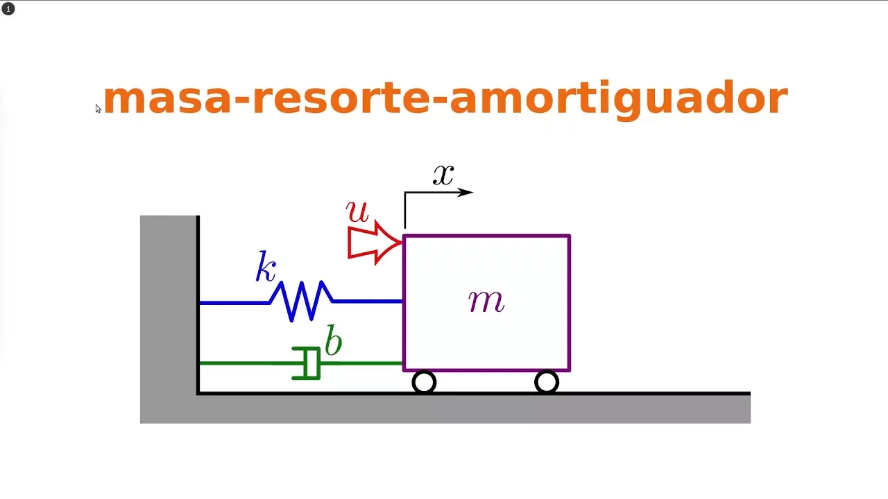
masa-resorte-amortiguador: ecuación diferencial y función de transferencia
166.9K
The mass-spring-damper system is modeled using Newton's second law, resulting in the second-order ODE: m*x'' + b*x' + k*x = F(t), where m is mass, b is damping coefficient, k is spring constant, x is displacement, and F(t) is external force; applying Laplace transform with zero initial conditions yields the transfer function G(s) = X(s)/U(s) = 1/(ms² + bs + k), representing the relationship between input force and output displacement in the s-domain.
Click to watch →

10 Physics Chapter 1🔥| SHM and Waves | Complete Chapter | 10th Physics | Oneshot | Faizan Tanveer
34.6K
In a mass-spring system, the acceleration (a) is given by a = -kx/m. This shows that acceleration is directly proportional to the displacement (x) and is always directed opposite to the displacement. Since k and m are constant, acceleration depends only on the displacement.
Click to watch →

Recap of Spring-Mass-Damper System Components
23.9K
A spring-mass-damper system consists of three fundamental components: mass (which resists acceleration according to Newton's second law F = m×a), damper (which dissipates energy proportional to velocity F = C×v), and spring (which stores potential energy proportionally to displacement F = K×x); these relationships can be analyzed in both time domain (using derivatives) and frequency domain (using Laplace transforms), with the governing equation being the sum of forces equals mass times acceleration (∑F = m×ẍ).
Click to watch →
Prerequisite Knowledge
- Concept 01Basic principles of Micro-Electro-Mechanical Systems (MEMS), specifically how mechanical structures are integrated on a silicon substrate.
- Concept 02The physics of capacitive sensing, including how displacement changes the capacitance of a differential capacitor structure.
- Concept 03Fundamentals of semiconductor manufacturing, particularly photolithography, silicon maskworks, and integrated circuit (IC) packaging.
- Concept 04The Newtonian physics of mass-spring-damper systems and how acceleration translates to mechanical displacement.
Subsequent Learning
- Step 01The evolution of MEMS design from early single-axis analog sensors to modern multi-axis (3-axis and 6-axis) digital Inertial Measurement Units (IMUs).
- Step 02Advanced semiconductor failure analysis and reverse-engineering techniques, such as Scanning Electron Microscopy (SEM) and Focused Ion Beam (FIB) circuit modification.
- Step 03Signal conditioning electronics for micro-sensors, including capacitive-to-voltage converters and on-chip amplification.
- Step 04Modern consumer and industrial applications of MEMS, ranging from smartphone screen rotation to automotive airbag deployment systems.
Part Intro
MEMS Core
Sensing Logic
Spec Limits
Part Intro
0:00Playing Section
- 1
Examines ADXL5 accelerometer in metal casing.
- 2
Uses Thor Labs opener to access internals.
The Multi-Chip Module (MCM) Integration Counter-Strategy
While the ADXL05 is celebrated as a pioneering monolithic MEMS device that integrated both the mechanical sensor and BiCMOS circuitry on a single silicon die, a major counter-perspective in semiconductor manufacturing favors the multi-chip module (MCM) approach. Critics of monolithic integration argue that combining micro-machining and advanced CMOS fabrication on a single wafer compromises both processes, leading to lower yields, higher development costs, and longer time-to-market. In contrast, the two-chip approach—housing a dedicated MEMS sensor die alongside a separate, optimized ASIC in a single package—allows for independent process optimization, better scalability, and lower overall production costs. This architectural debate shaped the evolution of the MEMS industry, with many modern high-volume sensors adopting the multi-chip strategy over the monolithic design pioneered by early devices like the ADXL05.
Deep Dive
The evolution of MEMS design from early single-axis analog sensors to modern multi-axis (3-axis and 6-axis) digital Inertial Measurement Units (IMUs).

Evolution of Bosch Inertial Measurement Units for Consumer Electronics
3.1K
Bosch Sensortec has developed three generations of Inertial Measurement Units (IMUs) for consumer electronics, demonstrating significant progress in MEMS design and technology: the BMI 055 (first generation) used a closed-loop architecture with four separate chips, the BMI 160 (first low-power IMU) introduced open-loop mode-split architecture with 40% die area reduction, and the BMI 260 (second low-power generation) achieved nearly 50% further size reduction through functional integration and dual-layer micromachining, while maintaining comparable noise performance and demonstrating key innovations like laser resealing for dual-pressure cavities and stress-insensitive sensor topologies.
Click to watch →

Inertial Measurement Unit (IMU) – A tiny sensor system with wide range of applications
693
An Inertial Measurement Unit (IMU) detects and measures movement in three-dimensional space using accelerometers, gyroscopes, and optionally magnetometers. Accelerometers measure linear acceleration along three axes (X, Y, Z), providing three degrees of freedom. Gyroscopes measure angular rotation around three axes (roll, pitch, yaw), adding three more degrees of freedom. Combined, these create six-axis IMUs; adding a magnetometer creates nine-axis IMUs for Earth magnetic field orientation. MEMS (Micro-Electro-Mechanical Systems) combines mechanical and electronic components in microscopic packages. MEMS accelerometers use suspended proof masses with polysilicon springs; acceleration causes displacement changing capacitance between electrodes. MEMS gyroscopes use the Coriolis effect: oscillating proof masses experience perpendicular forces during rotation. Structures are 100 times smaller than human hair (hundreds of nanometers to 300 micrometers), enabling fast response and mass production. Tuning fork configurations ensure angular rotation detection independent of linear acceleration.
Click to watch →
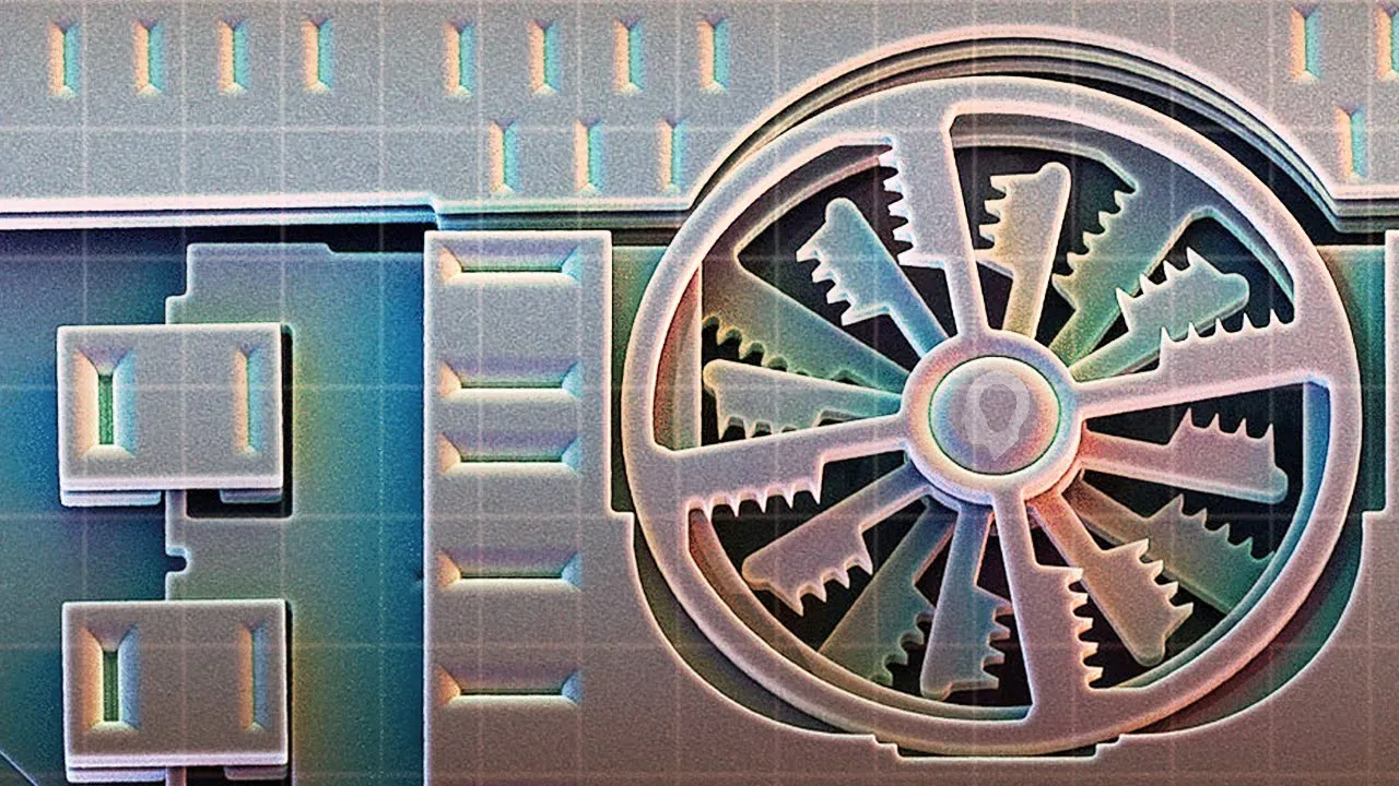
The Amazing World Of Microscopic Machines
324.1K
MEMS accelerometers measure rapid deceleration using capacitive sensing: a proof mass deflects under acceleration, creating differential capacitance that generates voltage signals processed by onboard circuitry. These devices replaced heavy mechanical ball-and-tube sensors weighing pounds and costing hundreds of dollars, with over half a billion units now in vehicle operation. Three-axis configurations suspend proof masses on microscopic springs with capacitive fingers detecting motion in all directions, enabling applications in earthquake detection, VR systems, pacemakers, and disk drives. MEMS gyroscopes exploit the Coriolis effect by suspending accelerometers on oscillating platforms—angular forces create perpendicular forces sensed by accelerometers and translated to rotational measurements. In thermal inkjet printing, resistive heaters rapidly heat ink to 100°C per microsecond, creating bubbles that eject droplets; bubble collapse creates vacuum pulling fresh ink. Piezoelectric alternatives use charged crystals vibrating to force ink out, with modern heads containing 600 nozzles achieving 1200 dpi resolution.
Click to watch →

Silicon Sensing 25-year timeline
144
This video traces the 25-year evolution of MEMS inertial sensor technology from its origins in 1998, when Silicon Sensing Systems was formed through the merger of Sumitomo Precision Products and Collins Aerospace, through key milestones including the invention of the first Coriolis vibrating structure gyroscope in 1985, the development of automotive electronic stability systems, the launch of the popular Pinpoint sensor series, and the release of industry-leading DMU sensors, demonstrating how MEMS technology has transformed navigation systems across automotive, aviation, and industrial applications worldwide.
Click to watch →

MEMS Micromachining Overview 9/9/2014
35.1K
Multi-axis accelerometers measure acceleration in multiple directions (X, Y, Z) and rotational axes (pitch, yaw, roll). Three-axis accelerometers detect linear acceleration, while six-axis versions add rotational sensing. These sensors enable sophisticated motion detection in automotive safety systems, smartphones, and drones. The integration of mechanical sensing elements with electronic readout circuits demonstrates the convergence of mechanical and electrical engineering in MEMS technology.
Click to watch →
Deep Dive
Advanced semiconductor failure analysis and reverse-engineering techniques, such as Scanning Electron Microscopy (SEM) and Focused Ion Beam (FIB) circuit modification.

FA Advanced Tech. & Techniques; Tools, Tech. & Techniques; Advanced Failure Analysis Case Studies.
409
This webinar presents five advanced failure analysis case studies demonstrating sophisticated analytical techniques for semiconductor and electronic device characterization: (1) Circuit modification using focused ion beam for reverse engineering, (2) Embedded defect analysis combining FIB, TEM, EDS, and EELS to identify oxidized nickel at layer interfaces, (3) Copper oxidation analysis employing optical microscopy, AFM, FIB, TEM, AES, XPS, and EELS to characterize oxide thickness and chemical states, (4) Surface contamination analysis using XPS survey scan and step profile to detect chromium and organic silicon contaminants, and (5) ToF-SIMS analysis for detecting surface contaminants at the parts per billion level. The presentation emphasizes that successful failure analysis requires selecting appropriate characterization techniques based on the analytical requirements, with different tools providing complementary information about elemental composition, chemical states, and structural characteristics of materials.
Click to watch →
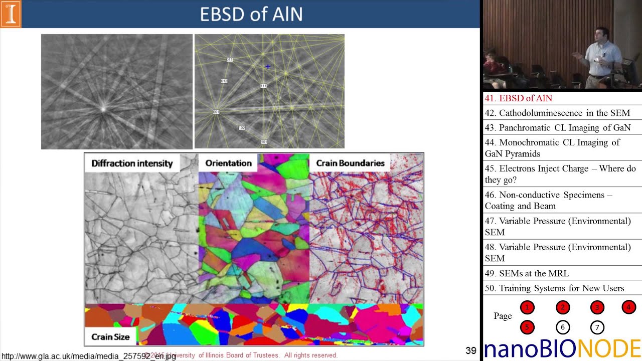
An Introduction to Scanning Electron Microscopy and Focused Ion Beam (Matthew Bresin)
79.9K
Scanning Electron Microscopy (SEM) uses a focused electron beam to image sample surfaces with 1-4 nm resolution, utilizing secondary electrons for topography, backscatter electrons for Z-contrast imaging, and characteristic X-rays for elemental analysis; the technique employs thermionic, field emission, or Schottky electron sources with electromagnetic lenses and various detectors including Everhart-Thornley, backscatter, EDS, WDS, EBSD, and cathodoluminescence systems, with resolution limited by chromatic aberration, spherical aberration, and diffraction effects that operators can partially correct through stigmator adjustments; sample charging in insulators is mitigated through coating, E2 point matching, or variable pressure/environmental SEM modes; the complementary Focused Ion Beam (FIB) technique enables precision milling, deposition, and TEM sample preparation through liquid metal ion sources with electrostatic lenses, allowing cross-sectional analysis and three-dimensional reconstruction of materials at nanoscale resolution.
Click to watch →

Microelectronics reverse engineering and market analysis (FULL VIDEO)
4.8K
Microelectronics reverse engineering involves systematically disassembling consumer electronics to analyze chips at multiple scales—from chip identification and disassembly to circuit reverse engineering and structural/materials analysis using advanced tools like scanning electron microscopes and ion beam mills, enabling detailed examination of chip layers as thin as one-thousandth of a human hair to reveal internal structures, dimensions, and materials used in semiconductor manufacturing.
Click to watch →
ASM EDFAS tutorial: SEM sample preparation for advanced semiconductor devices
107
Effective sample preparation for scanning electron microscopy (SEM) analysis of advanced semiconductor devices requires careful selection of techniques to minimize damage and preserve material integrity; mechanical polishing can cause surface damage up to three times the abrasive grit size, while focused ion beam (FIB) milling induces structural damage through atomic displacement and thermal effects, particularly problematic for thermally sensitive materials, making broad ion beam milling and automated delayering techniques essential for achieving artifact-free cross-sections and large-area layer removal with high uniformity.
Click to watch →

Failure Analysis Advanced Technologies & Techniques; - Semiconductor Failure Analysis Overview”
3.3K
Semiconductor failure analysis is a systematic process involving three main categories—electrical, physical, and material analysis—to identify root causes of device failures, utilizing various tools such as X-ray imaging, focused ion beam (FIB), and electron microscopy for defect localization and characterization.
Click to watch →
Deep Dive
Signal conditioning electronics for micro-sensors, including capacitive-to-voltage converters and on-chip amplification.

solution d'un examen module capteur pour licence 3
847
This section presents two fundamental signal conditioning circuits for sensor interfaces. The first circuit is a current-to-voltage converter that adapts a current source (equivalent to the sensor) to the measurement chain, with output voltage VM = -R × I. The second circuit is a charge amplifier that delivers voltage proportional to charge and independent of sensor capacitance, with VM = -Qc × Cf/Cc. Both circuits use operational amplifiers with virtual ground concepts to achieve precise signal conditioning. The charge amplifier's independence from sensor capacitance makes it particularly valuable for capacitive sensors where cable capacitance variations would otherwise affect measurements.
Click to watch →

Mod-05 Lec-36 Signal Conditioning Circuits and Integration of Microsystems and Microelectronics
757
Signal conditioning circuits are essential for converting raw sensor outputs into usable electrical signals. Three fundamental circuits serve different sensing modalities: (1) Wheatstone bridges amplify tiny resistance changes in piezoresistive sensors by creating unbalanced bridge conditions where output voltage V_out = (delta R/R) × V_in, enabling detection of micro-ohm-level resistance variations; (2) Switched capacitor circuits measure capacitive sensors by charging a known capacitor and transferring charge to the unknown capacitor, calculating capacitance from the resulting voltage; (3) Phase Lock Loops track frequency shifts in resonant sensors by comparing input frequency with a Voltage Controlled Oscillator, adjusting to maintain lock and detecting frequency changes indicative of applied forces or accelerations. These circuits form the bridge between physical phenomena and electronic processing in microsystems.
Click to watch →
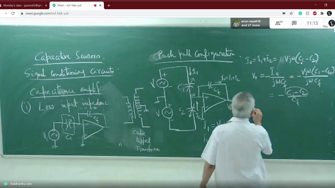
Capacitive Sensors | Signal Conditioning (1) | 19-10-2020
938
This lecture by Prof. S Sen from IIT Kharagpur's Department of Electrical Engineering covers essential signal conditioning techniques for capacitive sensors, including push-pull configurations in low-input impedance amplifiers, high-input impedance capacitance amplifiers, feedback-type capacitive amplifiers, and methods to mitigate parasitic capacitance effects in measurement systems.
Click to watch →

Lecture - 31 Interface Electronics for MEMS
8.2K
Microsensor signals exhibit defining characteristics requiring specialized interface electronics: extremely low amplitude in microvolt range, part-per-million level parameter changes, analog nature requiring ADC conversion, cross-parameter sensitivities where secondary effects (temperature) influence output, individual device output isolation needs, offset and linearity errors, and time-dependent output drift due to aging. Amplifiers serve as the primary signal conditioning block for microsensors producing DC signals in the microvolt range. Differential amplifier configurations are preferred for their ability to amplify DC signals while rejecting common-mode interference and power supply noise. However, offset voltage occurs due to component mismatch between matched pairs, with CMOS implementations showing 10-100 times worse performance than bipolar devices. Drift arises from temperature variations, aging, and mechanical stress during packaging. 1/f noise dominates at low frequencies in MOSFETs and is inversely related to frequency, making it particularly problematic for DC-coupled sensor interfaces.
Click to watch →
Introduction to Sensors (Full Lecture)
80.7K
Sensor outputs are often very tiny electrical signals requiring internal amplifiers to produce usable outputs. This amplification is one form of signal conditioning. Common sensor output formats include voltage signals (0-5V, 0-10V, -10V to +10V) and current signals (4-20mA). Signal conditioners may be external or integrated into sensors/systems.
Click to watch →
Deep Dive
Modern consumer and industrial applications of MEMS, ranging from smartphone screen rotation to automotive airbag deployment systems.

Ask The Expert: STMicroelectronics – MEMS and Predictive Maintenance | DesignSpark
32.7K
MEMS sensors evolved from simple accelerometers enabling smartphone portrait/landscape functionality to sophisticated multi-sensor systems. Early 4mm x 4mm form factors have decreased while accuracy improved, requiring careful accuracy-power trade-offs. MEMS technology converged across personal electronics, automotive (airbag deployment, electronic stability), and industrial sectors. Traditional bulky, expensive technologies were replaced by scalable MEMS solutions. Applications include Pokemon Go navigation, autonomous vehicle safe stopping requiring 20-centimeter accuracy, and biotechnology drug delivery. The technology enables capabilities previously impossible while maintaining affordable costs.
Click to watch →
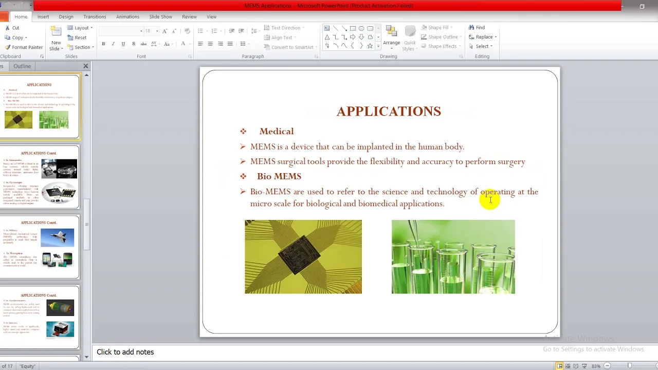
MEMS Applications (MEMS & NANO TECHNOLOGY) By Mr. Vibhu Goyal
2.1K
Micro-Electro-Mechanical Systems (MEMS) are microscopic devices that integrate mechanical elements, sensors, actuators, and electronics on a common silicon substrate, enabling revolutionary applications across diverse fields including consumer electronics (smartphones, gaming controllers), automotive systems (airbags, tire pressure monitoring), healthcare (pacemakers, diagnostic devices), environmental monitoring, and military/aerospace systems, where their miniaturization, low power consumption, and batch fabrication capabilities provide significant advantages over traditional macro-scale solutions.
Click to watch →

MEMS TECHNOLOGY – training program EUROPE - SESSION 1
224
MEMS applications span automotive (airbags, suspensions), consumer electronics (smartphones), biomedical (lab-on-chip, organ-on-chip), aerospace (gyroscopes for navigation), industrial (shock testing), and sports performance monitoring. Common MEMS devices include accelerometers, gyroscopes, pressure sensors, micro mirrors, and grippers. Silicon-based devices are common, while PDMS is preferred for soft microfluidic applications.
Click to watch →
MEMS Technology & its Applications
684
Smartphones contain multiple MEMS devices including mirrors for autofocus, display enhancement components, switches, tuners, oscillators, speakers, temperature sensors, imagers, haptic interfaces, humidity sensors, and pressure sensors for environmental sensing. In automotive applications, airbags (legally required), microphones for noise cancellation, distance detection systems for collision avoidance, airflow sensors, brake pressure sensors, tire pressure monitoring systems (TPMS), and exhaust sensors are essential. Autonomous driving requires even more sophisticated sensor suites.
Click to watch →

Kameroista 6G:hen, autoihin ja kehonmittauksiin - mikroskooppiset MEMS -laitteet (Suomi kärjessä)
1.4K
MEMS (Microelectromechanical Systems) combines electronics with microscopic mechanical structures like membranes, levers, and mirrors on a single chip. Manufacturing uses semiconductor techniques including thin film growth, lithography, and etching, but creates three-dimensional structures. The technology translates mechanical changes into electrical signals and vice versa. Originating from 1960s piezoresistive sensors, MEMS gained mass production in the 1990s with HP's inkjet cartridges, then exploded in smartphones and cars. Key applications span consumer electronics (motion sensors, microphones, speakers, VR displays), automotive systems (airbags, tire pressure monitoring, stabilization), and healthcare (wearable sensors for heart rate, temperature, breathing). Piezoelectric materials like PZT and Scandium-doped aluminum trioxide now enable more efficient sensors and actuators.
Click to watch →
Part Intro
MEMS Core
Sensing Logic
Spec Limits
Part Intro
0:00- 1
Examines ADXL5 accelerometer in metal casing.
- 2
Uses Thor Labs opener to access internals.
The Multi-Chip Module (MCM) Integration Counter-Strategy
While the ADXL05 is celebrated as a pioneering monolithic MEMS device that integrated both the mechanical sensor and BiCMOS circuitry on a single silicon die, a major counter-perspective in semiconductor manufacturing favors the multi-chip module (MCM) approach. Critics of monolithic integration argue that combining micro-machining and advanced CMOS fabrication on a single wafer compromises both processes, leading to lower yields, higher development costs, and longer time-to-market. In contrast, the two-chip approach—housing a dedicated MEMS sensor die alongside a separate, optimized ASIC in a single package—allows for independent process optimization, better scalability, and lower overall production costs. This architectural debate shaped the evolution of the MEMS industry, with many modern high-volume sensors adopting the multi-chip strategy over the monolithic design pioneered by early devices like the ADXL05.
Basic principles of Micro-Electro-Mechanical Systems (MEMS), specifically how mechanical structures are integrated on a silicon substrate.
The physics of capacitive sensing, including how displacement changes the capacitance of a differential capacitor structure.
Fundamentals of semiconductor manufacturing, particularly photolithography, silicon maskworks, and integrated circuit (IC) packaging.
The Newtonian physics of mass-spring-damper systems and how acceleration translates to mechanical displacement.
The evolution of MEMS design from early single-axis analog sensors to modern multi-axis (3-axis and 6-axis) digital Inertial Measurement Units (IMUs).
Advanced semiconductor failure analysis and reverse-engineering techniques, such as Scanning Electron Microscopy (SEM) and Focused Ion Beam (FIB) circuit modification.
Signal conditioning electronics for micro-sensors, including capacitive-to-voltage converters and on-chip amplification.
Modern consumer and industrial applications of MEMS, ranging from smartphone screen rotation to automotive airbag deployment systems.
3.7M views82.3Klikes1:09@EvilmonkeyzDesignzOriginal Release: 2025-04-18
Let's take a closer look at an accelerometer. Specifically, we'll be looking at the ADXL5 from Analog Devices. This accelerometer is unique in that it is mounted in a metal can. To open up these types of parts, I like to use the WR1 can opener from Thor Labs.
When the lid is almost separated, I pry it open manually in order not to damage the chip inside. The ADXL5 is a MEMS's device, which basically means that it has moving parts made of silicon. In this case, there's a center beam structure with comblike teeth on either side. This center structure is allowed to freely move in response to external forces, causing the teeth to move closer or further from nearby fixed teeth. This movement ultimately causes a change in capacitance, which can be sensed and interpreted as an acceleration. The data sheet has some really nice diagrams that show this in detail. This part can measure plus or minus 5g of acceleration, but only in a single axis.
If you want to measure all three axes at the same time, you need to have a total of three of these devices with each one oriented in a different sensing direction.
Up Next

1:00
MEMS Vibrating Structure Gyroscope: Inside the CRS03-01T Angular Rate Sensor.
@EvilmonkeyzDesignz
1.8M views•2024-04-08
30:32
Ultrasonic Transducers: Resonant Frequency Measurement and Horn Design
@imajeenyus42
229.9K views•2017-02-22

54:16
Polymer Environmental Degradation: Mechanisms & Stabilization
@iit
1.8K views•2012-07-10

33:39
How a Student's Question Saved a NYC Skyscraper from Collapse
@veritasium
22.8M views•2025-04-26
Related Study Plans & Knowledge Roadmaps
Structured learning paths in Engineering
engineering
Building Acoustic Levitators: Physics & Arduino
01The Physics of Sound and Standing Waves
02Piezoelectric Transducers and H-Bridge Drivers
03Arduino Programming: Generating 40 kHz Signals
+ 2 more learning modules
14h5 modules
Explore Roadmap
engineering
Building Peltier Cloud Chambers: Particle Tracks
01Cosmic Rays & Cloud Chamber Physics
02Thermoelectric Cooling (TEC) Fundamentals
03Custom Liquid-Cooling Loop Design
+ 2 more learning modules
18h5 modules
Explore Roadmap
engineering
Yagi-Uda Antennas: Modeling, Build & VNA Test
01Introduction to RF and Antenna Fundamentals
02Yagi-Uda Antenna Design Principles
03Antenna Modeling and Simulation in 4NEC2
+ 2 more learning modules
18h5 modules
Explore Roadmap
engineering
ECG Monitor Design: Op-Amps, Filters & Noise
01Electronics & Breadboard Basics
02Op-Amps and Instrumentation Amplifiers
03Bioelectricity and ECG Fundamentals
+ 2 more learning modules
18h5 modules
Explore Roadmap