













Graphene, a two-dimensional carbon material with sp2 hybridization and planar structure, exhibits exceptional electrical conductivity, mechanical strength, and thermal properties due to its unique Dirac electron behavior and zero-gap semiconductor characteristics. Chemical Vapor Deposition (CVD) on copper foil substrates, optimized by Lee in 2009 using methane gas at 1000°C under isobaric and isothermal conditions, produces high-purity monolayer graphene films that can be transferred to arbitrary substrates through chemical etching with iron nitrate and polymer coating methods. This scalable synthesis technique enables applications in electronics, sensors, energy storage, and as a growth template for other 2D materials like molybdenum disulfide and phosphorus.
Graphene Synthesis via Chemical Vapor Deposition (CVD) Techniques
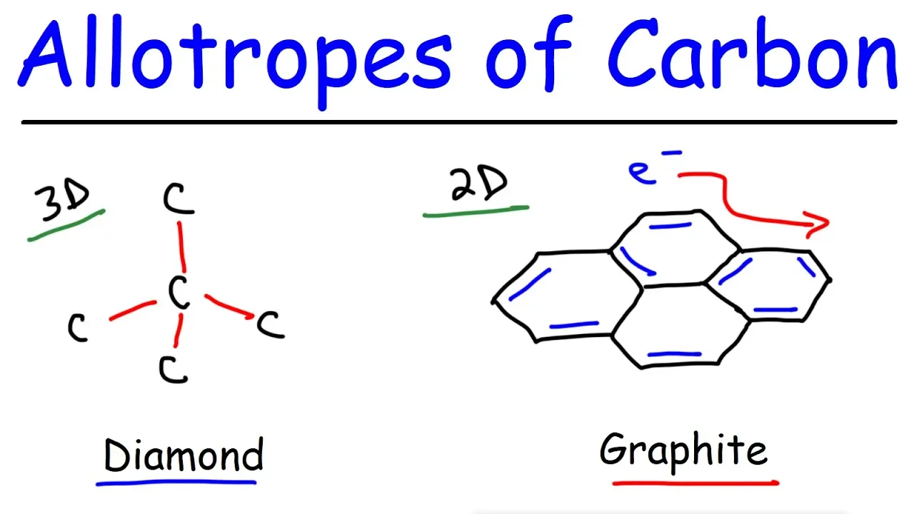
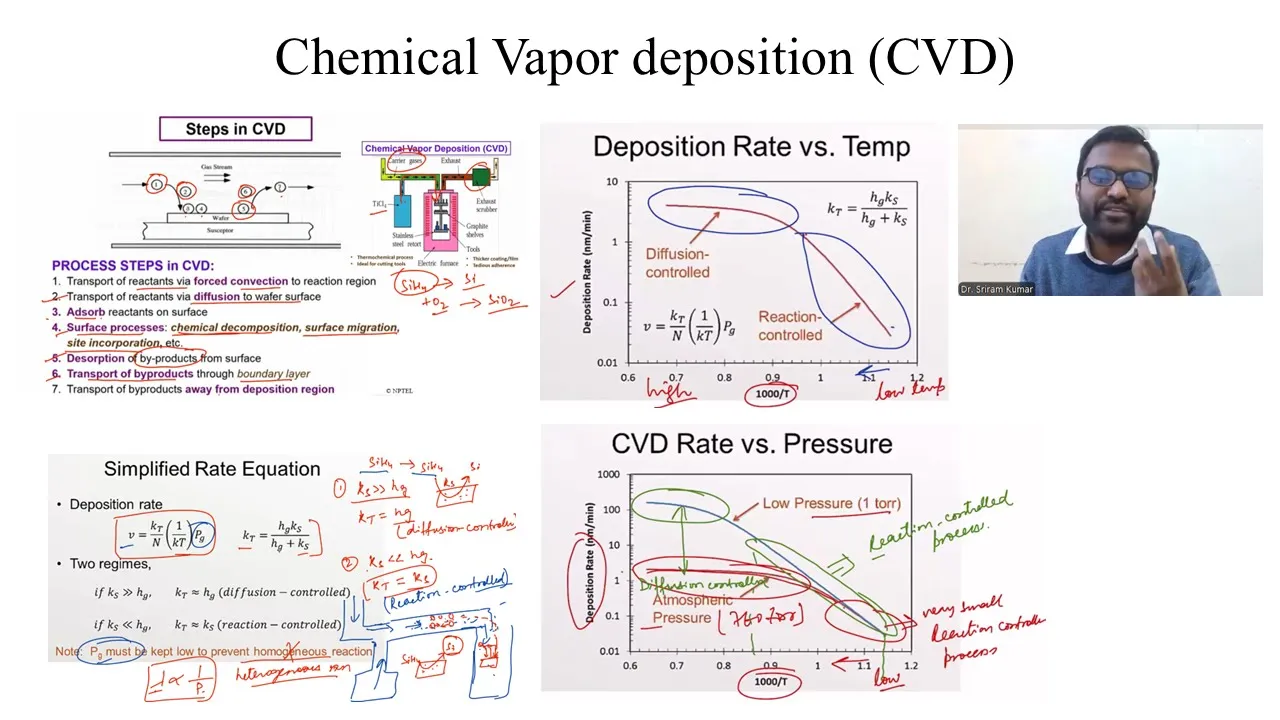
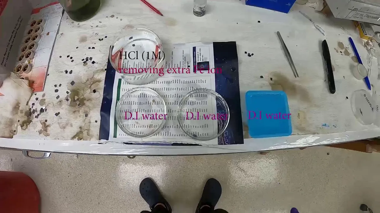
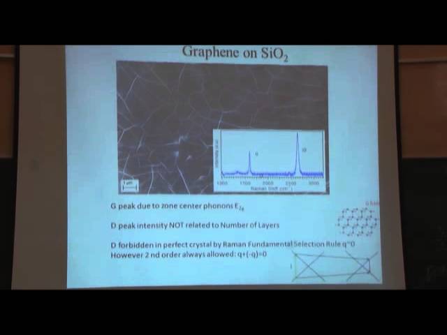
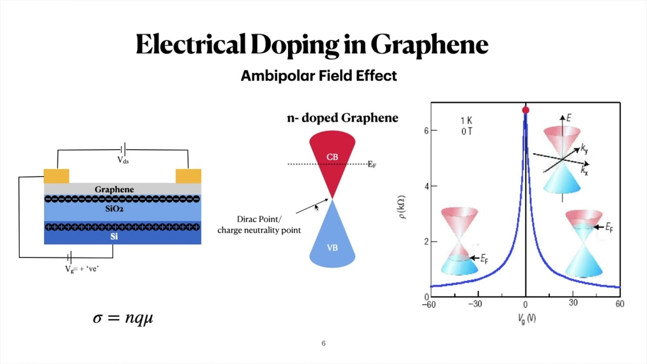
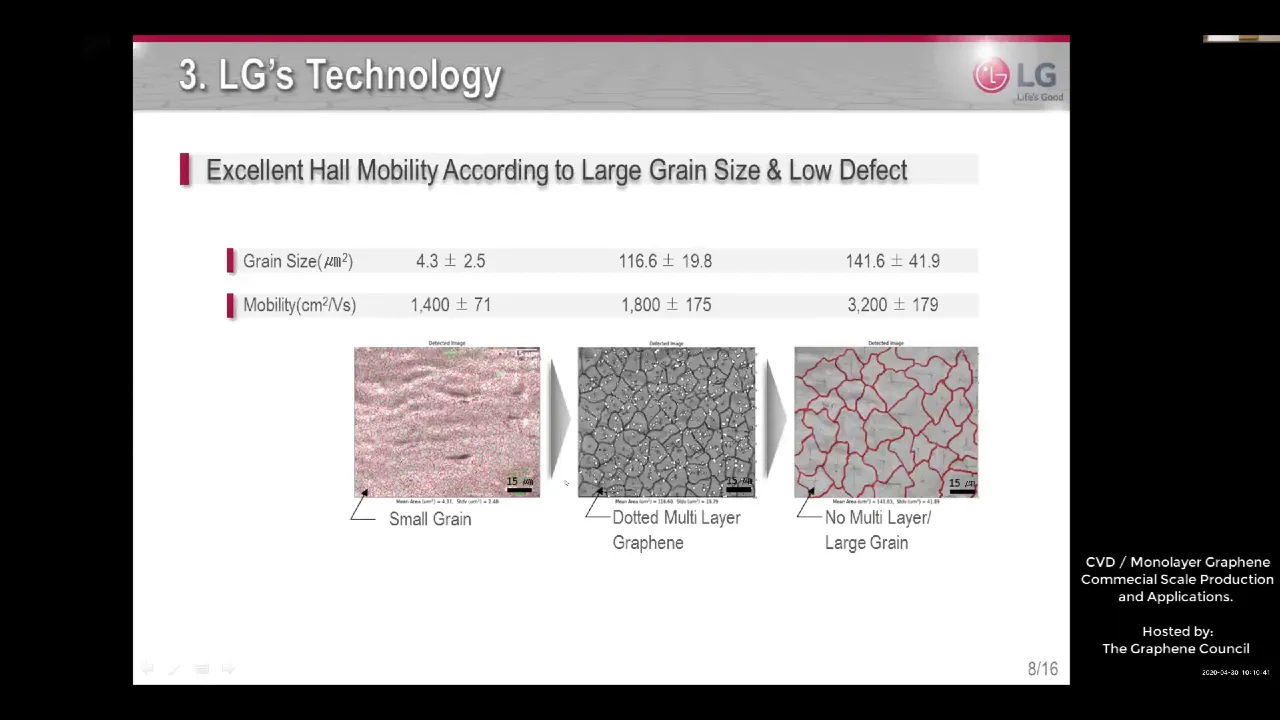
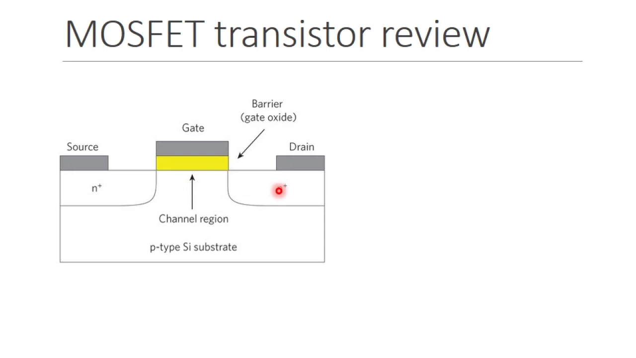
Added:hello my name is Seth Brody and for my inorganic research survey I chose the topic of graphing a survey of applied synthesis through chemical vapor deposition or CVD techniques so as an introduction in the modern endeavor of Technology the topic of scale is intrinsically limiting robust material properties nearly independent of such scale are being investigated for two-dimensional or 2d compounds such as graphene the dense sp2 hybridization and planar structure of this organic mono layer afforded superior conduction and visible absorption through surface Dirac electron behavior as well as mechanical paramount it also undergoes self repair and functionalization under conditioning these properties have been employed chiefly by the electronics industry originally discerned by micrometer scale mechanical exfoliation from natural graphitic service surfaces synthesis techniques have advanced to scalable growth methods that limit application among many such techniques chemical vapour deposition or CVD demonstrated distinct layer purity greatest area at centimeter scale as well as arbitrary substrate transfer which all contribute to effective Electronics application this CVD process was optimized by the reviewed experiment conducted by Lee in 2009 essentially using methane gas pressurized on the copper foil substrates under isobaric and isothermal conditions produced films works foliated by chemical etching with iron nitrate and then transferred through favored film foil pre coating process onto target ads orbing substrates coupled SEM and optical imaging Raman mapping and field effect transistor transistor or FEC analyses showed high monolayer purity and copper thickness independence for surface catalysis through self-limiting substrate solubility and saturation and reasonable quality via room temperature extracted carrier mobility in residual Dirac density but effective than mechanically exfoliated equivalents a later commercial process developed larger scale larger inch scale films conducted in 2010 graphene was also found to be viable as an oriented materials growth template yet inorganic molybdenum disulphide and phosphorus 2d materials were structurally favored for electronics application these of course were other examples of graphene's application and diverse purpose further massive energy conversions are necessary or at least considered in all physical processes the materials industry attempts to direct such pure phenomena to support technology and Leslie our sentient existence as this inherent understanding of the universe has grown its pursuit has inevitably arrived at maximized scale researchers and engineers are committing such accumulated knowledge to understand and apply processes of both parsec and Fermi scale distances both an expression and measurement scale is relevant to all dimensions and intersection of its nature yet this challenge to our existence requires materials that are robust on all scales with in the most recent centuries purely two-dimensional or 2d materials have presented transcendent physical and chemical properties that will enable technology enrichment as super materials planar organic sheets composed of a carbon lattice called graphene maintain properties which are structurally unique to is mono layer architecture as the first to D crystal discovered this molecule acts as the allotropic ie structural source of derived 0d fullerene spheroids 1d in nanotubes in the prominent stacked 3d graphite carbon allotropes the densely conjugated bonding within the sheet is sp2 hybridized as previously previously mentioned allowing unique electron-electron interactions across the mono layer surface the PZ electron of the half-filled bonding and anti-bonding pi bands increases electron ie charge carrier mobility therefore unlike those short shorter and metals this semi metal supports long-range interactions which affect various properties particularly electrical energy band conduction more specifically considered a zero gap semiconductor carrier energy is not constrained to promotion across the energy gap between discrete filled valence and empty conduction bands this phenomenon occurs via a Dirac points through which the electrons behave as quantum holes for such conductive scattering effects Dirac points represent this continuous band as and cones showing electron-electron range with greater interaction velocity near the cone is resecting de rock point as curvature when in an undamped charge neutral valence occupied state this phenomenon has been detected via angle resolved photo emission spectroscopy so due to such distinct conductivity this material maintains the highest known current density exceeding that of copper by a 1 million fold factor as well as intrinsic semiconductor mobility both conversely and expectedly resistivity is also lowest for graphene additionally graphite thermal conductivity is greatest while that of the similar 3d allotrope Karp and graphite is smaller by a factor of five as the thinnest material at 0.34 five nanometers graphene density is very low it is gas impermeable even to helium yet it's relatively high absorption a visible electromagnetic radiation is also governed by the low-energy structure evident at Dirac points through this low density largest volume surface ratio is achieved yet graph yet graphene is most thermodynamically stable and relatively large sheets at 80 nanometers or over 24 thousand atoms and its dense conjugation does not prevent flexible extension of the planar surface graphene is mechanically harder than carbon allotropes of homogeneous diamond crystals and heterogeneous steel alloy some of these properties are collectively demonstrated by a theorized nearly optically invisible graphene hammock supporting the mass of a housecat at 4 kilograms with hammock mass being that of its whisker less than 1 milligram although in their absorbing groups may be functionalized onto its surface as well as stacked in graphitic form for specialization and have damaged self-repair occurs under simple exposure to organics graphene was initially detected as electrical conductivity differences of intercalated graphite in the 1960s through this technique the sheets were isolated by large salt molecules such as a potassium salt containing THF and a you know an organic carbon chain in nmp solvent however complex techniques conducted from 1859 to 2004 weren't able to discern graphing crystals yet a simple method was finally able to do so only recently in 2004 a novel crystal isolation method called micro mechanical exfoliation was implemented to cleave the graphene crystals using common adhesive tape from a natural pyrolytic graphite surface this effective technique finally allowed further investigation of the unique crystal properties as previously discussed by the reproducible flakes generated this cleavage technique exploits the much weaker inter sheet Vander Waals interactions and those of the interest sheet covalent character within the stacked graphite architecture such isolation method progress was indicated by the exponential research public interest publication interest trend following this year by 2013 China had claimed 2216 inventions while the United States earned 1305 inventions in South Korea obtained eight 684 however patents claimed by respective companies or by respective company were 422 sent by Samsung Electronics 167 IBM and 124 LG Electronics by this activity interest in graphene has been rapidly growing with acute emphasis in the electronics industry the domain of electronics compromise comprises both diverse and broad applications graphene has been used in electrical devices sensors energy storage and composites yet application delimits necessary quality and scale of the material quality will be defined as mono layer purity in this topic survey for example electrical devices such as field effect transistors or F ETS require high quality but small area parameters but conductive coatings only demand low quality and area however touchscreens and solar cells require both high quality and large-scale films the execution of maximized scale is a synthesis challenge for commercial application but the chemical vapor deposition or CVD method has shown success and other techniques such as a reduction of graphite oxide and carbon nanotubes unzipping have been employed for the respective limited applications mentioned synthesis methods are also diverse but some additional examples are liquid phase extraction epitaxial growth on electrically insulating substrates such as silicon carbide and of course exfoliation exfoliation competes with CBD in terms of quality but is not a scalable technique the final substrate transfer process of CVD is also favorably arbitrary and Leslie not limited by application CVD synthesis can be performed on multiple substrates including transition metals and through various organic vapor ligands under many conditions but in 2009 the CVD method was established to produce large films on a copper foil substrate and were successfully transferred on to other arbitrary substrates in this experiment graphene films were primarily grown on thin 25 micron thick 1 centimeter long copper foils using a hot wall furnace of fused silica tube 22 millimeter inner diameter heated in a split tube configuration coils of 12.5 and 58 micrometer thickness were also considered where multiple runs were performed using each thickness the growth process began by evacuation of such foil loaded tube whose original pressure was replaced by then of hydrogen gas and at 40 milli Torr added at a maintained flow rate of 25 to SCCM for the entire process at 1000 Celsius degree Celsius the temperature of the copper foil substrate was finally stabilized at less than or equal to 1,000 degrees Celsius during this typical conditioning pre-process time interval of about 60 minutes and then the gaseous methane carbon source ligand was introduced to this copper surface at constant flow rate of 35 SCCM and total pressure of about 500 milli Torr this growth process principally occurred over a 30-minute interval under isothermal and isobaric conditions and followed by a furnace cooling to room temperature and about 60 minutes this cooling rate was also considered from 40 to greater than 300 degrees Celsius per minute the synthesized graphene films were separated and transferred from the coil of the copper foil substrate during the subsequent substrate dissolution process aqueous iron nitrate solution was used to exfoliate these produce films through chemical etching this effective chechik interval was determined by etching concentration as well as foil area and thickness usually a 1 square centimetre 25 micrometer thick copper foil was dissolved by iron nitrate overnight but this was at low concentrations of 0.05 grams per milliliter at about 16 hours overnight but this chemical exfoliation process collected two films from both sides of each copper surface the final substrate transfer step considered two similar approaches films were absorbed from the dissolved substrate by contact onto the arbitrary one and then the other approach the film foil system surface was first coated with poly dimethyl siloxane or PDMS or poly methyl methacrylate or PMMA and upon copper dissolution the remaining coated graphene was transferred by adsorption from solution as above or as previously mentioned further this conant transfer method was derived from and therefore similar to one that was also based on edged exfoliation in that original technique detachment of coated PMMA graphene as a system for the initial substrate was performed by mere partial itching of the substrate or silicon dioxide by sodium hydroxide at one molar concentration in an aqueous condition a room-temperature water bath allowed manual detachment of this membrane by peeling upon this release the graphene was then transferred to the target substrate by dissolving the PMMA with acetone while superimposing this final substrate the morphological and conductive properties of the produced films of in this reviewed experiment we're then primarily determined by coupled scanning electron microscopy or SEM and optical imaging which consisted of SEM and TEM mapped Raman spectroscopy on surface oxidized to silicon substrate and fabricated field effect transistor to summarize the growth and transfer processes the graphing films were grown on thin copper foils by direct surface catalysis hot wall furnace of a fused silica tube was used as the oven source of heat and iron nitrate edging exfoliated film storing substrate dissolution the growth process consisted of 8 the tube being evacuated and then back filled with gaseous hydrogen the stabilized copper temperature was next and then the gaseous methane was introduced at certain flow rate and pressure over over a given time that under isothermal and isobaric conditions there was cooling to room temperature and then for the transfer process in this experiment the system coated with PDMS or PD ma and solution occurred next and then after the copper dissolved the coated graphene was lifted from a solution and then upon this the subsequent transfer to new substrate of the surface oxidized silicon dioxide was the final step and the typical growth profile by condition is shown which summarizes these steps and the critical growth phase the coded transfer method was derived from a similar method as mentioned it is all it was also based on edged exfoliation it has previously described in summary there was a detachment of the coded PMMA graph graphene by a partial itching of the substrate silicon dioxide the water bath was used for a manual detachment by this peeling process and then transfer was to a superimposed target substrate and these steps are summarized in this graphic or this figure I should say as the original wet graphene transfer process so in terms of the conclusions of this experiment we will begin with the results of it the CVD deposition mechanism was expected to be precipitous by which foil thickness would determine surface layer density yet this behavior was not observed in this experiment imaging analyses instead presented mono layer purity greater than 95 percent and foil thickness independence of a surface catalyzed process through self-limiting copper substrate solubility and saturation Raman mapping indicated characteristic approximate 0.5 G to 2d intensity ratio where the G represented graphene structure and the symmetrical 2d band represented typical 2d planar structure as well as low defect intensity which was represented by the D band additionally the dual gated fe t device was constructed using a double layer of graphene separated by a thin layer of aluminum oxide dielectric material the subject graphene showed reasonable conduction by room temperature extracted carrier mobility of the border of ten to the third and residual to rock density of ten to the eleventh but was notably less effective than the mechanically exfoliated equivalents which were respectively at the ten to the fifth border and 10 to the 13th order so there was reasonable success however in these figures the effective deposition of graphene is shown through the gloss of the film as you'll note also in the second figure SEM and more SEM morphology and transfer on to two different arbitrary substrates are shown the SEM image represents a 30 minute duration growth period I mean and finally in the last SEM compilation or yeah compilation of induration was shown to affect the film growth or or the coverage of of the foil surface and as you will note it increases but then saturates after 10 minutes where where these images depict one the 60 minutes as mentioned the figure on the right figure 16 represents the f80 device and it's resistance versus top gate voltage or v TG and also in terms of the VD dirac top gate voltage which I would assume would be at the dirac point measured in terms of back gate voltage with the model fit which is represented by the solid line so over all coupled analytical methods determined film quality which was essential for this very thin surface that could be prone to these such defects so coupled methods really did show a true confirmation of the properties in the in the left figure or figure fifteen there there is an SEM image in a a microscope contrast uniformity depiction and B but when also in D and F the D G A to D mapped Raman peak bands are represented however the Sun the subset C seemed to be the most relevant to me I mean the the colored indications in a and B were represented through C which showed that the three different layers and how they are affected by the intent the intensities and their characteristic ratios for such structure specifically the Raman mapped layer bands and characteristic bands shifting and ratios are are presented in the subset C or Raman shift and verses or intensity versus Rama shift and finally commercial viability is a necessary consideration for development of new technology a later 2010 commercial process was developed and derived from these growth and transfer techniques resulting in larger one inch scale films also of high quality the adhesive roll-to-roll transfer by polymer support enables rapid dry transfer and rinse itching this method was applied through fabrication of low sheet resistance and high transparency doped four layer transparent electrodes which were therefore superior to commercial ones of indium tin oxide material high strain functional touchscreen panel devices were also produced using this process in conclusion graphene has pioneered the path for 2d super materials to research and industrial endeavors promoting maximized scale in terms of novel application graphene was also found to be viable as an oriented birth template for various materials supporting electrical applications such as solar cells super capacitors lithium-ion batteries and photocatalysis through these respective roles graphene acted as a growth self-assembly and sacrificial templates separately as well as contributed to surfactants or surface active agents such agents are used to mitigate interfacial surface interactions despite that the diverse properties and leslie robust applications of graphene in organic 2d materials such as molybdenum disulfide and phosphorus structurally compete for preferred electronics behavior with engineered graphene oxide via carrier mobility produced area high device on/off ratio of the molybdenum disulphide as well as tunable bandgap of phosphorus separately the research interest trend has been similar to the graphene as well there are four 2d materials largely afford unique properties to their application and have established a structural basis for the future of materials technology and with that thank you for your time and for considering this presentation I did enjoy learning these these properties of graphene and thank you for the opportunity and my name is Seth Brody thank you again and of course multiple references were used to develop this work and to really embody the the breadth of the efforts engaged in graphene however there were many more synthesis techniques and conditions with within them that should be scrutinized in further surveys but for the scope of this work which was truly a survey of methods before the the CBD on copper technique as well as after I believe that the the the requirements were met for a proper survey again thank you for your time and for your consideration
Up Next
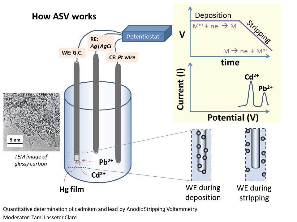
Anodic Stripping Voltammetry: Cadmium & Lead Analysis Lab
@tamiclare1604
51.1K views•2016-01-21

Frances H. Arnold Nobel Lecture: Directed Evolution in Chemistry
@NobelPrize
109.5K views•2018-12-08
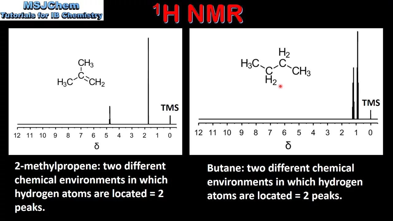
1H NMR: Determining Number of Peaks from Structure
@MSJChem
59.2K views•2017-04-06
Edible Water Bottles: A DIY Guide to Sodium Alginate Spherification
@ryan
10.5M views•2019-06-21
Related Study Plans & Knowledge Roadmaps
Structured learning paths in Chemistry