Localized Surface Plasmon Resonance (LSPR) is an optical phenomenon where conduction electrons on the surface of metal nanoparticles (like gold or silver) oscillate collectively when exposed to light at specific wavelengths, creating intense electromagnetic fields called plasmonic hotspots; this resonance is highly sensitive to environmental changes such as molecular binding, enabling real-time label-free detection of chemical and biological substances, and has significant applications in optical computing, compact sensors, and advanced optical components.
Localized Surface Plasmon Resonance (LSPR): Optical Sensing & Computing
Added:Deep Dive
Basic Electromagnetism and Light-Matter Interaction: Understanding Maxwell's equations and how electromagnetic waves interact with dielectric and conducting media.
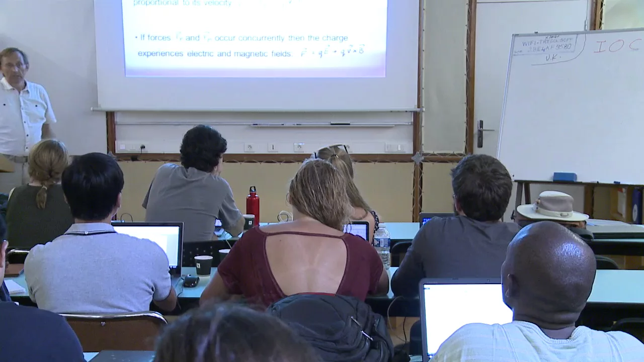
01 Dariusz Stramski Fundamentals of the Light Matter Interaction
2.6K
Light is described classically as coupled electric and magnetic fields perpendicular to each other and to propagation direction. Maxwell's equations unify field generation: electric fields from charges and time-varying magnetic fields, magnetic fields from currents and time-varying electric fields. These equations predict electromagnetic waves travel at speed c in vacuum, are transverse waves, and transport energy via the Poynting vector. Young's double-slit experiment provided wave evidence through interference fringes, demonstrating constructive and destructive interference patterns that only waves can produce.
Click to watch →

The Interaction of Light with Matter: microscopic picture. uvic Optics Week 3a
1.1K
Light interacts with matter through electric fields that accelerate charges. Key concepts include: (1) Transverse electromagnetic waves with perpendicular E and B fields, (2) Electric dipoles formed by separated charges, (3) Permanent dipoles in polar molecules like water, (4) Induced dipoles in neutral atoms where external fields separate positive and negative charges. These induced dipoles oscillate and re-radiate light, forming the basis for all optical phenomena including diffraction, scattering, and focusing.
Click to watch →

Nejvíce Uklidňující Fakta O Silách Přírody, U Kterých Usnete
801
Electricity, magnetism, and light are not separate phenomena but different manifestations of a single unified force called electromagnetism. James Clerk Maxwell discovered in the 19th century that changing electric fields create magnetic fields and vice versa. Together they form electromagnetic waves that travel through space at the speed of light. This single force explains everything from starlight to electrical wiring to lightning bolts, and it holds atoms together, enables molecular formation, and allows energy to spread freely through the universe. Electromagnetic waves can travel through a vacuum without requiring any matter to propagate. Electric and magnetic fields are two sides of the same invisible structure, constantly exchanging energy. Light, radio waves, and all electromagnetic radiation are simply different vibrations of this single field. Electromagnetism is the force that binds atoms together. In every atom, negatively charged electrons are attracted to the positively charged nucleus, creating balance. Without this attraction, electrons would fly away and matter would dissolve. At the same time, the electrical repulsion between protons in the nucleus would tear atoms apart if not countered by the strong nuclear force. Together, these forces create all the solid matter around us—walls, air, and our own bodies. Every color you see, every sound you hear, every texture you feel, every smell you detect, and every sensation of warmth from sunlight—all result from electromagnetic interactions between particles.
Click to watch →
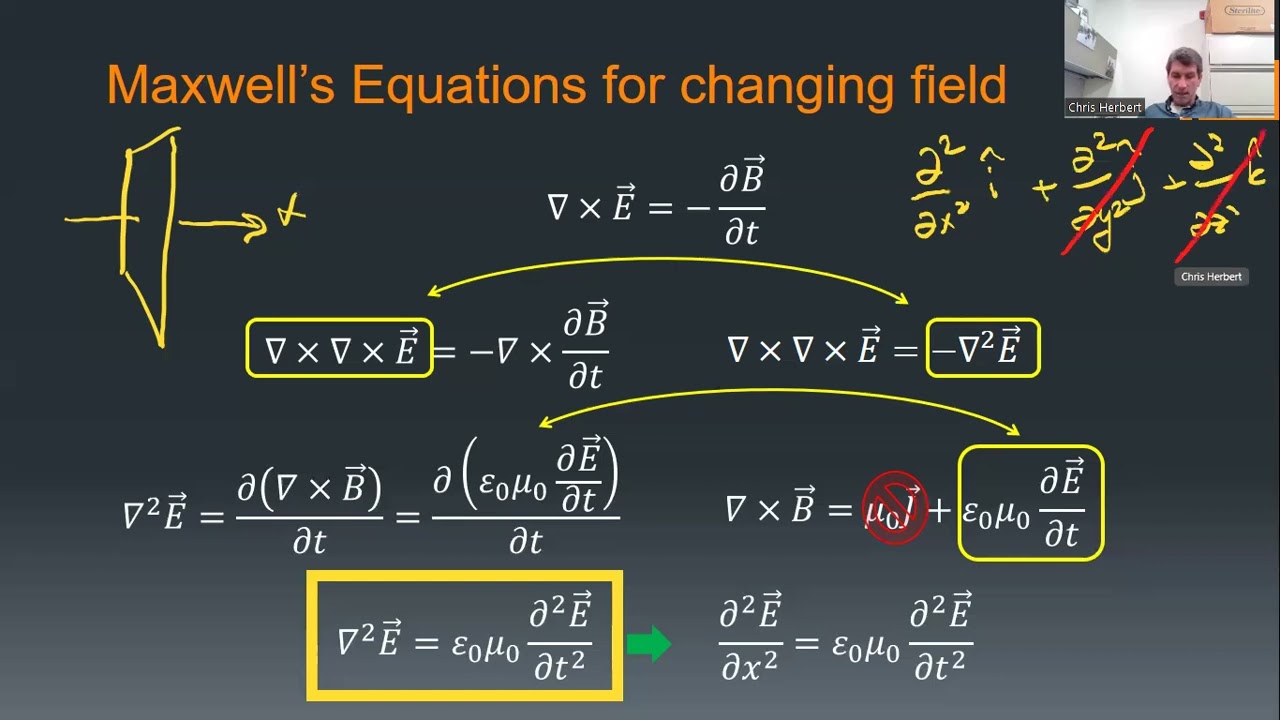
PHYS 230 Chap 16 Sec 2
2.6K
The speed of electromagnetic waves in vacuum is v = 1/√(μ₀ε₀), which equals the speed of light c (approximately 3 × 10⁸ m/s). This relationship shows that light speed is determined by fundamental electromagnetic properties of free space. Additionally, c equals the ratio of electric field to magnetic field in an electromagnetic wave, indicating that the electric field is much stronger than the magnetic field. This has important implications for light-matter interaction: the electric field has a much stronger impact on electrons in atoms than the magnetic field, which is why the electric field is primarily responsible for how light interacts with matter.
Click to watch →
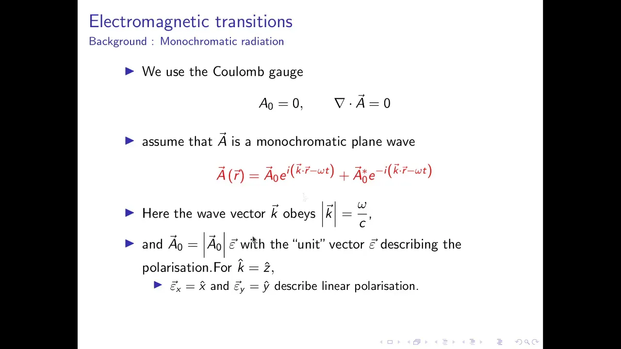
09 Interaction of light with matter - a time dependent perturbation theoretic treatment
1.4K
This comprehensive section establishes the classical electromagnetic foundation for understanding light-matter interactions. The semi-classical approach treats atoms as quantum mechanical entities while electromagnetic radiation is treated as an external classical field, explaining approximately 99% of optical phenomena without requiring photons. Key topics include minimal coupling modifying kinetic energy to (p - eA/c)²/(2m), the Coulomb gauge condition (∇·A = 0) simplifying calculations, monochromatic plane wave representations with polarization vectors ε, and the Poynting vector giving energy flow with intensity I = (1/2)(ω²/c)|A₀|²k̂. Incoherent radiation with randomly distributed phases eliminates cross-mode terms, simplifying multi-frequency calculations. These classical foundations enable subsequent quantum mechanical treatments of light-matter interactions.
Click to watch →
Deep Dive
The Drude Model of Metals: Familiarity with the free-electron model and how conduction electrons in metals behave under oscillating electric fields.

Drude Model | Free Electrons
74K
The Drude model, developed by Paul Drude in 1900, treats electrons in metals as free particles that move between scattering events, with the equation of motion given by dp/dt = F - p/τ, where F is the applied force (such as electric or magnetic fields) and τ is the average scattering time; this simple kinetic theory successfully explains many properties of metals despite its crude assumptions about electron behavior.
Click to watch →

Mod 3 | Lec 1: The Drude model of metals - Part I
383
Metals possess distinct properties: high electrical conductivity (σ, Siemens/meter) due to conduction electrons, high thermal conductivity (κ, W/m·K) from electron motion, malleability and ductility, and electronic specific heat that increases linearly with temperature (C_e ∝ T). The Wiedemann-Franz Law states κ/σ = LT, where L = (π²/3)(k_B²/e²) is the universal Lorenz number. In metals like sodium, valence electrons become 'itinerant' (wandering throughout the material) when atoms form a metal, creating conduction electrons. The Drude model (1900) describes metals as: (1) Immobile positively charged ionic cores in a lattice, (2) A 'sea' of conduction electrons moving freely. Key assumptions: electrons collide elastically with ionic cores, move in straight lines between collisions, and the average time between collisions is the relaxation time (τ). The model employs the free electron approximation, neglecting electron-ion and electron-electron interactions.
Click to watch →

Solid State Physics | Lecture 2: Debye Model
25.5K
This section introduces the Drude model, the first successful theory explaining metallic conductivity. Before 1897, the nature of electricity was unknown. After Thomson's electron discovery, metals were understood to contain free electrons behaving like a gas. The Drude model treats electrons classically with three key assumptions: (1) electrons undergo scattering events with characteristic time τ; (2) after scattering, momentum resets to zero; (3) between scatterings, electrons obey Newton's law with applied forces. This yields the transport equation dp/dt = F - p/τ, where the drag term -p/τ represents scattering effects. Despite its crude nature, the model successfully explains many transport phenomena, demonstrating how simplified kinetic theory can capture essential physics of complex many-body systems.
Click to watch →

Lecture -- Drude Model for Metals
9.2K
The Drude model for metals is derived from the Lorentz oscillator model by eliminating the restoring force (setting resonant frequency to zero), where free electron density replaces bound electron density, and mean collision time τ replaces the damping coefficient γ; this model predicts that metals exhibit negative real permittivity below the plasma frequency (acting as good conductors with high reflectivity) and behave like transparent media above the plasma frequency, with conductivity decreasing with frequency according to σ(ω) = σ₀/(1 + jωτ), where σ₀ is the DC conductivity.
Click to watch →

The Drude Model
15.8K
The Drude model uses a bed of nails to represent the metal lattice, with each nail symbolizing a positive atomic nucleus. Electrons are visualized as balls that roll down inclined planes representing electric fields. When voltage is applied (one side raised), electrons accelerate toward lower potentials but constantly collide with nails, losing energy and bouncing back. This mechanical analogy explains why electrons don't achieve high speeds despite electric fields - their average drift velocity is extremely slow (about 1 mm/s). The model demonstrates that electrical conduction involves continuous acceleration interrupted by collisions, with energy dissipated as heat and light when electrons strike atoms.
Click to watch →
Deep Dive
Fundamentals of Wave Optics: Concepts of resonance, absorption, scattering, and the physical meaning of the refractive index.
PLUS TWO PHYSICS - MINI MARATHON | Xylem Plus Two
110.8K
Wave optics treats light as a wave phenomenon. A wave front is a collection of points at the same phase of vibration. Wave fronts are classified into three types: spherical (from point sources), cylindrical (from linear sources), and plane (from sources at infinity). Huygens' Principle states that every point on a primary wave front acts as a source of secondary wavelets, and the new wave front is the tangential surface to all secondary wavelets. This principle explains wave propagation and is used to derive laws of reflection and refraction.
Click to watch →

One Shot Revision Wave Optics Chapter - 10 I Full Chapter in 1 Video I Boards 2024 Class 12 Physics
90.4K
Optics is the study of light, which exhibits dual nature - traveling in straight lines (particle nature) and in wave form (wave nature). Electromagnetic waves are transverse waves with perpendicular vibrations. Wave optics deals with interference and diffraction phenomena. A wavefront is the continuous locus of all particles vibrating in the same phase. Three types of wavefronts exist: (1) Spherical wavefront from point sources spreading in all directions; (2) Cylindrical wavefront from linear sources spreading perpendicular to the line; (3) Plane wavefront formed at large distances when amplitude decreases due to medium resistance. A ray of light is an arrow drawn perpendicular to the wavefront, indicating propagation direction. Rays are always perpendicular to wavefronts with 90-degree angles. The time taken to travel between wavefronts is equal along any ray. Huygens' principle states that every point on a wavefront acts as a source of secondary disturbances spreading in all directions with light speed. New wavefronts are formed by joining forward tangents of secondary waves, while backward wavefronts are impossible as intensity in backward direction is zero.
Click to watch →

Wave Optics Mega Marathon | Boards के सबसे Important Questions |100/100 Strategy 💯 by Ashish Sir
45.6K
This section covers the foundational concepts of wave optics. Wave properties include wavelength (λ), phase angle (φ), and frequency (f), while the medium is not a wave property. A wavefront is defined as a surface where all points are in the same phase of vibration. Huygens' principle states that every point on a wavefront acts as a source of secondary spherical wavelets, and the new wavefront is the tangential surface to all these wavelets. This principle explains wave propagation, reflection, and refraction geometrically.
Click to watch →

WAVE OPTICS in 1 Shot: All Concept & PYQs Covered | Class 12th Boards | NCERT
509.8K
This comprehensive section covers the historical development of light theories and wave optics fundamentals. Newton's Corpuscular Theory (1637) proposed that light consists of tiny particles called corpuscles emitted by luminous sources, traveling in straight lines at the speed of light (3 × 10^8 m/s in vacuum). Different colors correspond to different corpuscle sizes. Huygens' Wave Theory (1678) challenged this by proposing light is a wave phenomenon. A wavefront is the locus of all points vibrating in the same phase. Three types of wavefronts exist: spherical (from point sources), cylindrical (from linear sources), and planar (from sources at infinity). Huygens' Principle states that every point on a wavefront acts as a secondary source of spherical wavelets. This principle successfully explains reflection and refraction through geometric relationships between wavefronts.
Click to watch →

Lecture -1 || 7. Wave Optics Physics Class 12th #Conceptbatch New Indian era #nie HSC Board
111.7K
Wave Optics is a physics chapter studying the nature and behavior of light. The chapter addresses fundamental questions: what light is, how it travels, and what scientists discovered about it. Light is a natural phenomenon enabling vision - without it, we cannot observe anything. Light consists of tiny particles called corpuscles (Newton's discovery). Light travels in straight lines and exhibits multiple properties during propagation: reflection, refraction, interference, diffraction, and polarization. The speed of light is approximately 3 × 10^8 m/s in vacuum, determined through experiments by multiple scientists.
Click to watch →
Deep Dive
Introduction to Nanomaterials: Understanding how physical and optical properties of materials change when scaled down to the nanometer level.

Nanomaterials
297
Nanomaterials are materials with at least one dimension in the nanometer scale (1 billionth of a meter), serving as the cornerstone of nanoscience and nanotechnology. They are synthesized through two main approaches: top-down (slicing bulk materials) and bottom-up (building from atoms/molecules). Key properties include dramatically increased surface area leading to enhanced catalytic activity, size-dependent electronic band changes causing conductors to become semiconductors/insulators, and reduced melting points due to fewer neighboring atoms. Applications span nanofibers for tissue engineering, nanosensors for pollution monitoring and medical diagnostics, and energy devices like fuel cells. The Indian government launched the Nano Mission in 2007 to promote research, human resource development, and national/international collaboration in this interdisciplinary field.
Click to watch →

Introduction to NanoMaterials
95.9K
Nanomaterials are defined as materials with at least one dimension between 1-100 nanometers, and they can be classified based on origin (natural or synthetic), material type (organic or inorganic), and dimensionality; natural nanomaterials occur in nature while synthetic ones are human-made, with engineered nanomaterials being deliberately fabricated for specific applications.
Click to watch →

Introduction to Nanomaterials - Nanoscience and Nanotechnology - Engineering Physics 2
53.7K
Nanomaterials are materials with particles in the nanometer scale (10^-9 meters), where one nanometer equals one billionth of a meter and is ten times larger than an angstrom (10^-10 meters); nanoscience studies the behavior of these materials, while nanotechnology involves fabricating structures at this scale.
Click to watch →

Nanomaterials lecture 1
338
Nanomaterials are materials where at least one dimension is between 1-100 nanometers. Richard Feynman, the father of nanotechnology, proposed in his 1959 lecture 'There's Plenty of Room at the Bottom' that atoms could be manipulated. Nanomaterials exhibit fundamentally different properties than bulk materials due to their high surface area to volume ratio and quantum effects. For example, bulk gold is non-magnetic and yellow, but gold nanoparticles become ferromagnetic and change color. The band gap in semiconductors can be engineered by reducing size, increasing conductivity. These properties enable applications in fabrics, batteries, medical devices, and energy production. Nanomaterials are classified into natural (viruses, butterfly wings), incidental (engine exhaust, fumes), and engineered (carbon nanotubes, quantum dots, graphene).
Click to watch →
ENGINEERING CHEMISTRY LECTURE 07 ''Introduction to Nanomaterials'' By Dr. Niti Maheshwari, AKGEC
11.1K
Nanomaterials are materials with at least one dimension in the nanoscale (1-100 nm), exhibiting unique properties such as quantum size effects, surface effects, and macroscopic quantum tunneling that differ from bulk materials. These materials can be synthesized through top-down approaches (reducing bulk materials to nano-scale) or bottom-up approaches (building from individual atoms/molecules). Common nanomaterials include fullerenes (discovered in 1985, Nobel Prize 1996), carbon nanotubes (cylindrical nanostructures with exceptional electrical and mechanical properties), and nanowires. Applications span electronics (quantum dots, carbon nanotubes), medicine (cancer treatment, drug delivery), energy storage, environmental remediation, and advanced manufacturing.
Click to watch →
Prerequisite Knowledge
- Concept 01Basic Electromagnetism and Light-Matter Interaction: Understanding Maxwell's equations and how electromagnetic waves interact with dielectric and conducting media.
- Concept 02The Drude Model of Metals: Familiarity with the free-electron model and how conduction electrons in metals behave under oscillating electric fields.
- Concept 03Fundamentals of Wave Optics: Concepts of resonance, absorption, scattering, and the physical meaning of the refractive index.
- Concept 04Introduction to Nanomaterials: Understanding how physical and optical properties of materials change when scaled down to the nanometer level.
Subsequent Learning
- Step 01Surface-Enhanced Raman Spectroscopy (SERS): Exploring how localized electromagnetic fields from plasmonic nanoparticles amplify Raman signals for single-molecule detection.
- Step 02Plasmonic Biosensors and Diagnostics: Studying practical applications in label-free, real-time detection of biomolecules, pathogens, and chemical analytes.
- Step 03Photonic and Plasmonic Computing: Investigating the design of optical logic gates, nanophotonic circuits, and ultra-fast optical computing architectures.
- Step 04Metamaterials and Metasurfaces: Learning how engineered nanostructures can manipulate light in unconventional ways, such as flat lenses or optical cloaking.
LSPR Basics
Applications
LSPR Basics
0:03Playing Section
- 1
Explains LSPR as electron oscillation in metal nanoparticles.
- 2
Resonance depends on particle size, shape, metal, and environment.
- 3
Creates strong electromagnetic fields and plasmonic hotspots.
All-Dielectric Nanophotonics (Mie-Resonance-Based Nanophotonics)
While Localized Surface Plasmon Resonance (LSPR) in metallic nanoparticles offers strong light confinement, it is severely limited by high intrinsic ohmic losses (absorption) and subsequent heat generation. This photothermal effect can damage delicate biological samples in sensing and degrade efficiency in optical computing. To address these limitations, "All-Dielectric Nanophotonics" has emerged as a major competing paradigm. By utilizing high-refractive-index dielectric nanoparticles (such as silicon or germanium) that support Mie resonances, researchers can achieve comparable light-matter enhancement at the nanoscale without the thermal losses associated with metals. Dielectric resonators offer much higher Quality (Q) factors, negligible heating, and compatibility with standard CMOS fabrication, making them a highly viable, and often superior, alternative for both ultra-sensitive label-free biosensing and low-power, high-efficiency optical computing devices.
Deep Dive
Surface-Enhanced Raman Spectroscopy (SERS): Exploring how localized electromagnetic fields from plasmonic nanoparticles amplify Raman signals for single-molecule detection.

What Is Surface-Enhanced Raman Spectroscopy (SERS)? - Science Through Time
241
Surface-Enhanced Raman Spectroscopy (SERS) is an analytical technique that dramatically increases the sensitivity of Raman spectroscopy by utilizing electromagnetic and chemical enhancement mechanisms at metal surfaces or nanostructures, enabling detection of substances at extremely low concentrations including single molecules; discovered in 1973 at the University of Southampton and formally named in 1979, SERS has become essential in biomedical diagnostics, environmental monitoring, and materials science for real-time, label-free molecular identification.
Click to watch →
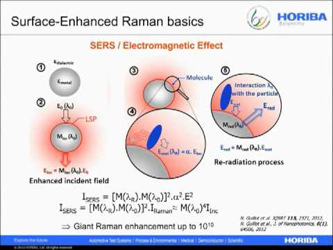
Basic Principles of Surface Enhanced Raman Scattering Theory by HORIBA Scientific
67.4K
SERS enhances Raman scattering signals from molecules located near nanostructured metallic surfaces when excited by visible light. This technique becomes essential when classical Raman spectroscopy fails due to low molecular efficiency or insufficient sample quantities. SERS offers two critical advantages: exceptional sensitivity for detecting trace amounts of substances, and molecular specificity through unique spectral fingerprints. The technique finds applications in chemistry and biology for contaminant detection in food/water and biomarker identification for cancer diagnosis. Three factors govern SERS performance: the substrate (noble metal nanoparticles), target molecule characteristics, and instrumental conditions including wavelength selection.
Click to watch →

What Is Surface-enhanced Raman Scattering (SERS)? - Chemistry For Everyone
257
Surface-enhanced Raman scattering (SERS) is a powerful analytical technique that dramatically amplifies Raman spectroscopy signals by placing molecules near nanostructured metal surfaces (typically gold or silver), enabling detection of substances at parts-per-billion concentrations; this enhancement occurs through two primary mechanisms: electromagnetic enhancement, where surface plasmons create intense localized electric fields called 'hot spots' that can boost signals by factors of 10^10 to 10^14, and chemical enhancement, where molecular interactions with the metal surface alter electronic structures to further amplify signals; SERS finds extensive applications in chemical analysis, biosensing, and catalysis, demonstrating how nanomaterials bridge physical chemistry and materials science principles.
Click to watch →

Introduction to Raman Spectroscopy
286
Surface Enhanced Raman Scattering (SERS) provides 10¹³-fold enhancement through electromagnetic field enhancement on rough metallic surfaces (silver, gold, aluminum). Surface plasmons are excited on rough surfaces, creating localized enhanced fields. Enhancement is greatest when laser frequency matches surface plasmon resonance frequencies, which depend on roughness dimensions and shape. Spherical particles have one resonance peak, rod-shaped particles have two, and prismatic particles can have three. SERS has two enhancement mechanisms: electromagnetic (10⁶-10¹⁴ enhancement, works up to 10nm from surface) and chemical (10²-10⁴ enhancement, requires direct contact). SERS enables detection of single molecules, quenching fluorescence, and studying molecular orientation and binding modes. Applications include studying proteins, viruses, and other biological samples that would otherwise produce undetectable signals.
Click to watch →

PGR Lab Primer - Surface enhanced Raman spectroscopy
25.4K
Surface Enhanced Raman Spectroscopy (SERS) is a powerful analytical technique that dramatically amplifies Raman signals by utilizing nanostructured metal surfaces to create intense electromagnetic fields, enabling detection of molecules at extremely low concentrations; this enhancement occurs when light excites surface plasmons at metal-dielectric interfaces, with structured substrates like sphere segment void (SSV) templates combined with nanoparticles achieving enhancement factors of up to 10^9-10^10 times compared to conventional Raman spectroscopy, making it applicable for portable drug testing and other sensitive detection applications.
Click to watch →
Deep Dive
Plasmonic Biosensors and Diagnostics: Studying practical applications in label-free, real-time detection of biomolecules, pathogens, and chemical analytes.

EuroTechTalk #1: Nanophotonic and single-molecule biosensing at EPFL and TU Eindhoven
970
A portable plasmonic biosensor uses a gold thin film perforated with nanoholes (approximately 200 nm diameter, 600 nm periodicity) operating in the visible wavelength range. When nanoparticles comparable in size to the nanoholes are introduced near the holes, they quench the extraordinary optical transmission (EOT) signal locally. The sensor functionalizes the surface with capture antibodies and nanoparticles with detection antibodies. Upon target binding, nanoparticles accumulate at nanohole locations, producing a measurable plasmonic signal. This system achieves detection limits of tens of picograms per milliliter with four orders of dynamic range, using standard CMOS cameras and visible LEDs for low-cost portable operation.
Click to watch →
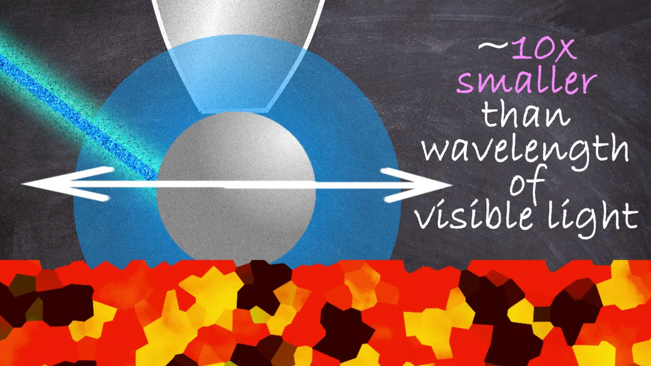
Tours Through Physics: Nanoplasmonics (Part 2), Sensing, Science and Diagnostics
13.7K
Nano plasmonic biosensors enable ultra-sensitive detection of specific molecules through selective binding interactions. By coating nanoparticles with biological ligands that bind exclusively to target analytes, researchers create sensors where the binding event itself produces a measurable signal change. When analytes attach to ligands on nanoparticles, the altered local environment causes a resonant frequency shift that can be visually detected. Home pregnancy tests exemplify this principle, using gold nanoparticles coated with HCG-binding ligands that change color from green to red upon hormone binding. These sensors achieve remarkable sensitivity, detecting analytes at femtogram concentrations—potentially enabling implantable medical devices for continuous glucose monitoring and security applications for explosive residue detection.
Click to watch →

Surface Plasmon based Biosensors-ELL212
4.2K
Surface plasmon resonance (SPR) is a phenomenon where electromagnetic waves couple with electron oscillations at the interface between a metal and a dielectric material, enabling label-free detection of biomolecular interactions by monitoring changes in the resonance angle caused by variations in the local refractive index; this principle forms the basis of biosensors that detect biological molecules without requiring chemical labels, providing accurate measurements of binding kinetics, concentration, and specificity.
Click to watch →

Optica Online Industry Meeting: Biosensing
710
This section presents two innovative biosensor platforms for rapid infection diagnosis: Biolum's CMOS-compatible plasmonic biosensors and ICN2's interferometric biosensors. Biolum has developed CMOS-compatible plasmonic biosensors using aluminum nanostripes on silicon nitride waveguides achieving E. coli detection down to 10 cells/mL and CRP detection in serum samples (1-40 μg/mL) with detection times under 30 minutes. The self-referencing design enables high sensitivity while canceling common-mode noise. ICN2 has developed interferometric biosensors operating in the visible range with multiplex configuration achieving picomolar limit of detection without amplification. Time-to-result is less than 30 minutes per test, transforming sepsis diagnosis from days to under an hour. Both platforms support multiplex detection of multiple targets on a single chip, addressing the critical challenge of antimicrobial resistance by enabling rapid pathogen identification and antibiotic susceptibility testing directly from patient samples at the hospital bedside.
Click to watch →

Comparing LSPR and SPR for Diagnostics - LamdaGen
68K
Surface Plasmon Resonance (SPR) and Localized Surface Plasmon Resonance (LSPR) are both optical biosensing technologies that utilize the interaction between light and metal surfaces to detect biomolecular interactions, but they differ significantly in their operational principles and practical applications: SPR requires complex instrumentation with adaptive optics to satisfy momentum conservation conditions and has a large sensing volume (up to 1,000 nm) that causes significant bulk effects and false positives from unbound molecules; in contrast, LSPR operates with simple instrumentation using white light and detectors, has a much smaller sensing volume (only ~40 nm) resulting in minimal bulk effect, and is more suitable for diagnostic applications due to its temperature independence, compatibility with complex biological matrices, and ability to achieve high sensitivity and quantitative precision in point-of-care settings.
Click to watch →
Deep Dive
Photonic and Plasmonic Computing: Investigating the design of optical logic gates, nanophotonic circuits, and ultra-fast optical computing architectures.

The Wire Problem Nobody In AI Is Talking About
91.2K
Modern AI training clusters require tens of thousands of GPUs communicating billions of times per second through collective communication. Copper interconnects face three fundamental problems at scale: resistance generates heat that dominates engineering decisions, signal loss degrades fidelity over distance, and energy per bit accumulates meaningfully when moving petabytes of data. These constraints compound together with each hardware generation, creating a physical ceiling that limits AI cluster growth. Photons offer a revolutionary alternative: they carry no electrical charge, generate no resistive heat, and maintain signal integrity over distance. Through wavelength division multiplexing, dozens of independent data streams can travel simultaneously through a single optical channel. Optical Processing Units encode data as light intensity, phase, or wavelength, performing matrix multiplications directly in the optical domain at the speed of light. MIT research demonstrates over 90% energy reduction for certain operations compared to electronic equivalents, fundamentally changing AI infrastructure economics.
Click to watch →

The Genius of Computing with Light
51.6K
Photonic quantum computing uses light instead of supercooled atoms or exotic particles. Qubits are encoded in the path of photons traveling through silicon waveguides—100nm ridges carved using semiconductor lithography. A qubit exists as a superposition of being in both paths simultaneously until measured. Photons are ideal qubits because they experience no time (traveling at light speed) and have decoherence times exceeding the age of the universe, unlike matter-based qubits with nanosecond-scale decoherence. This enables quantum computations that maintain coherence over extended periods.
Click to watch →

КАК РАБОТАЕТ ФОТОННЫЙ ПРОЦЕССОР | РАЗБОР
116.5K
Photonic computing represents a transformative paradigm shift from electronic to optical signal processing. Unlike traditional silicon processors that use electrons, photonic systems use photons (light particles) for data transmission and processing. Key advantages include: (1) Non-interacting photons enable multiple simultaneous signals through single channels, dramatically increasing throughput; (2) Significantly lower energy consumption and heat generation. Photonic technology is already used in smartwatches for health monitoring and fiber optic internet for high-speed data transmission. The first optical computer prototype appeared in 1990, with current research aiming for 10^21 operations per second. Current challenges include reconfiguration difficulties and scalability limitations. The practical solution is optoelectronic hybrid processors combining transistors for calculations with photons for data transmission. Companies like Lightmatter and Intel are advancing this field, with Intel demonstrating processors capable of 528 parallel threads with 1.2 billion transistors at only 75W. This technology is particularly valuable for machine learning and AI applications where electronic technologies are approaching fundamental limits.
Click to watch →

Meet Taichi — The Light-Speed Computer
267.6K
Photonic computing uses light instead of electrons for computation, enabling data processing at femtosecond speeds through light interference (constructive/destructive) and diffraction; the Taichi chip combines both techniques to achieve 1000x energy efficiency over conventional GPUs while performing AI tasks like image classification with 92% accuracy and generative AI operations.
Click to watch →

Moore's Law is Dead — Welcome to Light Speed Computers
3.2M
While fiber optics revolutionized global communication since the 1960s, using light to actually perform computations proved far more challenging. Scientists have envisioned optical computers since the 1980s because light offers inherent advantages: it travels at the speed of light with minimal energy loss and generates less heat than electrical signals. However, controlling light for computation is extraordinarily difficult—light naturally spreads and scatters, resisting confinement to tiny spaces or sharp directional changes. LightMatter has pioneered the integration of photonic components directly into computer chips, creating platforms like Passage that enable unprecedented data transmission rates and represent the first commercial-scale implementation of this transformative technology.
Click to watch →
Deep Dive
Metamaterials and Metasurfaces: Learning how engineered nanostructures can manipulate light in unconventional ways, such as flat lenses or optical cloaking.
Lec 2: Introduction to Metamaterials and Metasurfaces
14.5K
Metamaterials are artificially engineered materials whose electromagnetic properties are determined by their physical structure rather than their chemical composition, enabling the creation of extraordinary electromagnetic responses not found in natural materials; these materials consist of sub-wavelength meta-atoms (artificial atoms) that can be designed to exhibit properties like negative refractive index, allowing applications such as cloaking, sub-diffraction imaging, and wave manipulation across the entire electromagnetic spectrum from microwave to optical frequencies, while metasurfaces represent the two-dimensional counterpart of metamaterials, offering similar electromagnetic control within extremely thin layers.
Click to watch →

Metamaterials and Metasurfaces
153
Metamaterials are engineered materials with electromagnetic properties not found in nature, characterized by simultaneously negative permittivity (ε) and permeability (μ), which enables negative refractive index and phenomena like negative refraction. Metasurfaces are two-dimensional structures that manipulate electromagnetic waves through phase discontinuities at their interface, enabling applications such as flat lenses, beam steering, high-gain antennas, orbital angular momentum generation, and radar cross-section reduction. These structures achieve wavefront control using subwavelength resonators that provide local phase and amplitude modulation, offering advantages over bulk metamaterials including reduced dimensionality, lower loss, and easier fabrication.
Click to watch →
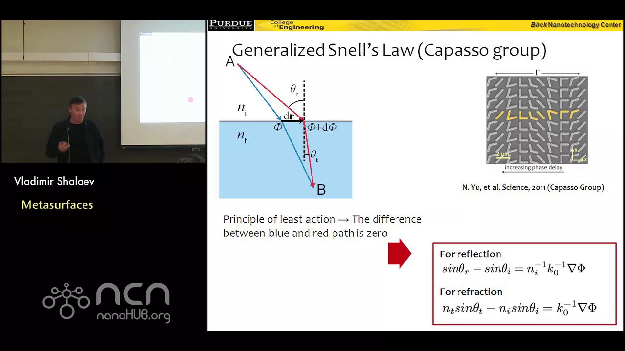
Nanophotonics & Metamaterials L1.3: Metasurfaces
17.5K
Metasurfaces are two-dimensional metamaterials that enable flat optics by abruptly controlling the phase of light through subwavelength antenna arrays, breaking traditional momentum conservation laws and allowing light to propagate in arbitrary directions; this technology extends to four-dimensional photonics when combined with time-varying materials near the epsilon-zero point, enabling ultrafast optical switching and non-reciprocal light propagation.
Click to watch →
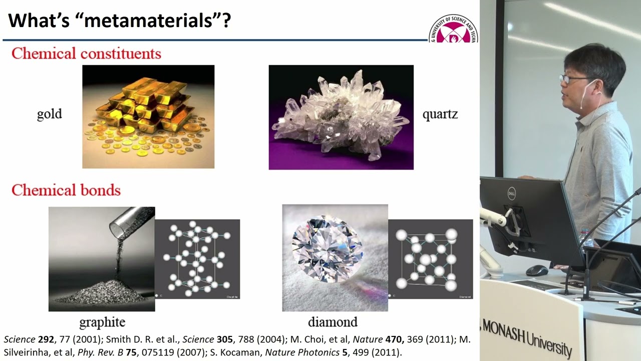
Metamaterials: from invisibility cloak to future extended reality displays & smart label technology
837
Metamaterials are artificially structured materials where electromagnetic properties emerge from engineered nanostructures rather than atomic composition. The scientific definition distinguishes them from chemistry-based materials: metamaterials derive properties from meta-atoms and their arrangement. Key electromagnetic phenomena include refractive indices up to 10,000, hyperbolic dispersion, negative refraction, perfect lensing, and invisibility cloaking. Theoretical proposals by Veselago (1968) preceded practical demonstrations until nanofabrication advances enabled split-ring resonator structures (Smith, 2001) and infrared implementations (Valentine). Classical refractive optics faces fundamental limitations: physical thickness constraints prevent smartphone integration, refractive lenses suffer spherical aberration, and diffractive optics face manufacturing difficulties. Metasurfaces solve these problems by using subwavelength nanostructure arrays that manipulate light through engineered phase responses. Flat metalenses using silicon nanorod arrays achieve focusing comparable to curved lenses while eliminating spherical aberration and reducing thickness dramatically. Advanced applications include 180° structured light projection for depth sensing, AI-optimized holograms achieving 91% efficiency, structural color for smart labeling, and humidity-responsive security features. Manufacturing scalability requires addressing bottlenecks through material engineering (engineered silicon, spin-coatable polymers), nanoimprintable polymers with embedded nanoparticles, lithography-based wafer-scale replication, and computational post-processing algorithms.
Click to watch →
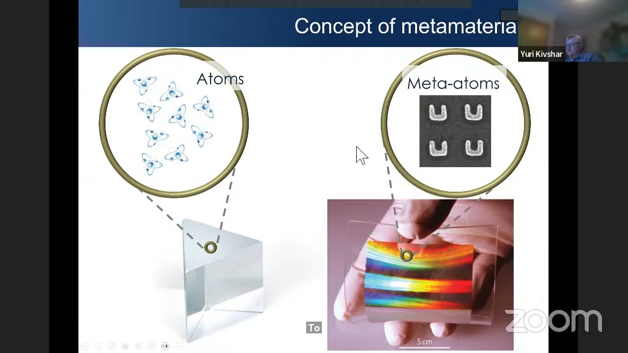
Prof. Yuri Kivshar - Meta^3: Metamaterials, Metaphotonics, and Metasurfaces
364
Metamaterials are artificially engineered materials composed of subwavelength structural elements called meta-atoms that can achieve electromagnetic properties not found in nature, such as negative refractive index; these concepts have evolved into metasurfaces—planar arrays of resonant nanostructures that enable precise control of light propagation, polarization, and phase, with applications ranging from invisibility cloaking and flat optics to quantum photonics and hyperspectral sensing.
Click to watch →
LSPR Basics
Applications
LSPR Basics
0:03- 1
Explains LSPR as electron oscillation in metal nanoparticles.
- 2
Resonance depends on particle size, shape, metal, and environment.
- 3
Creates strong electromagnetic fields and plasmonic hotspots.
All-Dielectric Nanophotonics (Mie-Resonance-Based Nanophotonics)
While Localized Surface Plasmon Resonance (LSPR) in metallic nanoparticles offers strong light confinement, it is severely limited by high intrinsic ohmic losses (absorption) and subsequent heat generation. This photothermal effect can damage delicate biological samples in sensing and degrade efficiency in optical computing. To address these limitations, "All-Dielectric Nanophotonics" has emerged as a major competing paradigm. By utilizing high-refractive-index dielectric nanoparticles (such as silicon or germanium) that support Mie resonances, researchers can achieve comparable light-matter enhancement at the nanoscale without the thermal losses associated with metals. Dielectric resonators offer much higher Quality (Q) factors, negligible heating, and compatibility with standard CMOS fabrication, making them a highly viable, and often superior, alternative for both ultra-sensitive label-free biosensing and low-power, high-efficiency optical computing devices.
Basic Electromagnetism and Light-Matter Interaction: Understanding Maxwell's equations and how electromagnetic waves interact with dielectric and conducting media.
The Drude Model of Metals: Familiarity with the free-electron model and how conduction electrons in metals behave under oscillating electric fields.
Fundamentals of Wave Optics: Concepts of resonance, absorption, scattering, and the physical meaning of the refractive index.
Introduction to Nanomaterials: Understanding how physical and optical properties of materials change when scaled down to the nanometer level.
Surface-Enhanced Raman Spectroscopy (SERS): Exploring how localized electromagnetic fields from plasmonic nanoparticles amplify Raman signals for single-molecule detection.
Plasmonic Biosensors and Diagnostics: Studying practical applications in label-free, real-time detection of biomolecules, pathogens, and chemical analytes.
Photonic and Plasmonic Computing: Investigating the design of optical logic gates, nanophotonic circuits, and ultra-fast optical computing architectures.
Metamaterials and Metasurfaces: Learning how engineered nanostructures can manipulate light in unconventional ways, such as flat lenses or optical cloaking.
339 views2likes3:12@EmergingTechInsiderOriginal Release: 2025-05-10
What is localized surface plasmon resonance LSPR? Have you ever wondered how tiny particles can have such a big impact on technology? Let's talk about localized surface plasmon resonance often referred to as LSPR. This fascinating phenomenon occurs when conduction electrons on the surface of metal nano particles like gold or silver start to oscillate together when they encounter light at certain wavelengths. These oscillations are not just random. They are confined to the surface of the nano particles creating what we call plasmonic hotspots. This means that the electromagnetic fields generated in these areas are incredibly strong. The magic of LSP are happens because of the interaction between light and the free electrons in these tiny metal structures. When light hits the nano particles, the electrons resonate at a frequency that depends on several factors. These include the size and shape of the particle, the type of metal, and even the environment around it. This resonance leads to enhanced absorption and scattering of light at specific wavelengths which can be measured and detected easily. From the perspective of emerging computing technologies, LSPR is quite important.
It allows four highly sensitive optical detection methods. The resonance condition is very sensitive to changes in the local refractive index near the nano particle surface. So when molecules bind to or interact with the nanop particles, the LSPR signal shifts. This shift enables real time labelfree detection of various chemical or biological substances. LSPR finds numerous applications in optical computing and plasmonics. It supports the development of compact and efficient sensors and devices. For instance, sensors based on LSP are can be integrated with optical fibers to detect biochemical interactions with remarkable sensitivity and specificity. These sensors are small, cost effective, and can operate in real time without needing complex labeling procedures. In the realm of optical computing, LSPR can be used to manipulate light at the nanocale. This capability leads to faster and more efficient data processing and communication technologies. The strong localization of electromagnetic fields around nano particles enhances light matter interactions which is essential for creating next generation optical components like switches, modulators and sensors. In essence, localized surface plasmon resonance is a fascinating optical effect where metal nano particles resonate with incoming light.
This effect produces enhanced electromagnetic fields and is highly sensitive to environmental changes. As a result, LSPR serves as a powerful tool for sensing applications and holds great promise for advancing optical computing technologies.
Up Next

186:48
Sean Carroll's Mindscape AMA August 2022: Physics, Society, AI
@seancarroll
109.9K views•2022-08-01

12:53
21cm Hyperfine Transition in Neutral Hydrogen: Radio Astronomy Basics
@AaronRobertParsons
12.4K views•2011-10-13

32:32
NMR Spin Physics I: Zeeman Effect, Resonance Condition & Larmor Frequency
@nptel-indianinstituteofsci8064
2.3K views•2024-01-17

27:14
Entropy and the Second Law of Thermodynamics Explained
@veritasium
27.5M views•2023-07-01
Related Study Plans & Knowledge Roadmaps
Structured learning paths in Physics
physics
Nuclear Physics (Decay, Fission & Reactors)
01Atomic Structure and the Binding Force
02Radioactive Decay and Half-Life
03Nuclear Fission Mechanics and Chain Reactions
+ 2 more learning modules
12h5 modules
Explore Roadmap
physics
Soft Matter (Polymers, Colloids & Rheology)
01Foundations of Soft Matter & Thermal Forces
02Polymer Physics and Macromolecules
03Colloids, Surfactants, and Self-Assembly
+ 2 more learning modules
38h5 modules
Explore Roadmap
physics
Analytical Mechanics: Lagrangian & Hamiltonian
01Mathematical Foundations: Calculus of Variations
02From Newtonian Mechanics to Constraint Dynamics
03The Principle of Least Action & Lagrangian Mechanics
+ 3 more learning modules
28h6 modules
Explore Roadmap
physics
General Relativity (Spacetime & Cosmology)
01Foundations of Relativity: Special Relativity
02The Geometry of Spacetime: Equivalence Principle & Curvature
03Einstein's Field Equations: The Mathematics of Gravity
+ 2 more learning modules
55h5 modules
Explore Roadmap