Nanomaterials are materials with particles in the nanometer scale (10^-9 meters), where one nanometer equals one billionth of a meter and is ten times larger than an angstrom (10^-10 meters); nanoscience studies the behavior of these materials, while nanotechnology involves fabricating structures at this scale.
Introduction to Nanomaterials | Engineering Physics 2 Lecture
Added:Deep Dive
Basic understanding of the metric system, scientific notation, and scale of measurements (micrometer, nanometer, angstrom).

Pasaje de unidades - Micrómetros, nanómetros, angstroms ¿Qué son?
8.1K
This section introduces measuring microscopic objects like viruses and molecules that cannot be seen with the naked eye. The metric system uses prefixes to indicate scale: 'micro-' means one millionth (10^-6) and 'nano-' means one billionth (10^-9). Key relationships include: 1 millimeter = 1,000 micrometers, 1 millimeter = 1,000,000 nanometers, and 1 nanometer = 10 angstroms. These relationships allow scientists to choose appropriate units for different objects, keeping numbers manageable and easy to interpret.
Click to watch →

MIX QUESTIONS, PHYSICS VARG - 3 2025 NOTIFICATION | MPTET VARG-3 2025 VACANCY | MPTET VARG 3 2025
13.1K
This section covers length measurement scales: Fermi (10^-15 m) measures atomic nuclei; Angstrom (10^-10 m) measures atomic/molecular scales; Nanometer (10^-9 m) measures nanotechnology; Micrometer (10^-6 m) measures microscopic objects; Millimeter (10^-3 m) measures small objects. The smallest commonly used unit is the fermi, used for nuclear physics measurements.
Click to watch →

فيزياء تانيه ثانوى الترم الاول 2026 | الدرس الاول فيزياء تانية ثانوي الترم الاول | شرح صيغه الابعاد
153.6K
Scientific notation simplifies large and small numbers: 100 = 10², 0.1 = 10⁻¹, 1,000,000 = 10⁶, 0.001 = 10⁻³. Metric prefixes express multiples or fractions: nano (10⁻⁹), micro (10⁻⁶), milli (10⁻³), kilo (10³), mega (10⁶), giga (10⁹), femto (10⁻¹⁵). To convert between metric units, multiply by the appropriate power of 10. For example, meters to millimeters is ×10³, millimeters to meters is ×10⁻³. Compound unit conversions require converting each unit separately. The 'round and return' method involves: (1) First convert to the base unit (e.g., meters), (2) Then convert from the base unit to the target unit. Mass units follow the same rules. The femtosecond (fs) is 10⁻¹⁵ seconds, discovered by Ahmed Zewail for measuring ultra-fast chemical reactions. Area units are squared: 1 cm² = 10⁻⁴ m². Volume units are cubed: 1 cm³ = 10⁻⁶ m³. The angstrom (Å) is 10⁻¹⁰ meters, used for atomic and molecular scales.
Click to watch →

RRB NTPC & Group D Science Classes | Railway ALP & Group D Science Practice Set 01 | by Saurabh Sir
143.7K
One nanometer equals 10⁻⁹ meters. One micrometer (micron) equals 10⁻⁶ meters. One angstrom equals 10⁻¹⁰ meters. One millimeter equals 10⁻³ meters. These units are essential for measuring very small distances in physics and chemistry.
Click to watch →

UNIDAD 01 - Niveles de organizacion biologicos y ecologicos - BIOLOGIA INGRESO A MEDICINA UNCUYO
2.3K
Biology uses metric units: Meter (base), centimeter, millimeter, micrometer (10^-6 m), nanometer (10^-9 m), angstrom (10^-10 m), picometer (10^-12 m). Scientific notation is used to handle very small or large numbers. The human eye can resolve objects about 100 micrometers; optical microscopes reveal down to ~10 nanometers; electron microscopes can visualize structures as small as 1 angstrom.
Click to watch →
Deep Dive
Fundamental concepts of atomic structure, chemical bonding, and crystal lattices from introductory physics and chemistry.

Задание №4 | Химическая связь и кристаллические решетки | ЕГЭ по химии 2025
18.1K
This comprehensive lesson covers the fundamental concepts of chemical bonds and crystal lattices in chemistry. The main topics include: (1) Covalent bonds - nonpolar (H2, Cl2, N2, O2) and polar (HCl, H2O, HNO3) types, (2) Ionic bonds forming between active metals and non-metals, (3) Molecular ions (NH4+, SO42-) with covalent bonds within, (4) Crystal lattice types - molecular (ice, sugar), atomic (diamond, graphite), ionic (NaCl), and metallic (copper, iron), (5) Classification of substances by bond types, (6) States of matter and molecular motion. Understanding these concepts is essential for comprehending the relationship between atomic structure and chemical behavior.
Click to watch →

physics , Atomic structure and chemical bonding (5)
910
Atoms consist of three fundamental particles: protons (positive charge, located in the nucleus), neutrons (neutral charge, located in the nucleus), and electrons (negative charge, orbiting in shells around the nucleus). The atomic number equals the number of protons, while the mass number equals the sum of protons and neutrons. Chemical bonds include ionic bonds (between metals and non-metals through electron transfer), covalent bonds (between non-metals through electron sharing), metallic bonds (between metal atoms through a sea of delocalized electrons), and weaker secondary bonds like hydrogen bonds and van der Waals forces. Crystalline solids have ordered atomic arrangements with sharp melting points, while amorphous solids have disordered arrangements without sharp melting points. Crystal defects include point defects (vacancies, interstitials, impurities), line defects (dislocations), and surface defects (grain boundaries).
Click to watch →

Строение атома. Строение вещества. Химическая связь.
1.2K
This lesson covers the fundamental principles of chemical bonding and atomic structure. Substances are classified as amorphous or crystalline, with crystalline substances having atomic, molecular, or metallic lattices. Metallic bonds hold atoms in metallic lattices, ionic bonds hold ionic lattices, and covalent bonds form in atomic and molecular lattices. Covalent bonds are non-polar when identical non-metal atoms bond, and polar when different non-metal atoms bond. Ionic bonds form between metal and non-metal atoms. Electronegativity determines bond type, with non-metals having higher values. Electronegativity increases across periods (increasing nuclear charge, outer electrons, decreasing radius) and decreases down groups (increasing energy levels, radius). Atomic structure is determined by proton count (nuclear charge), with neutrons also present in the nucleus.
Click to watch →

Dental BioMaterials 1 ; Lec 1 ; Structure of Matter
335
Atoms consist of a nucleus (protons and neutrons) surrounded by electrons in shells. Valence electrons determine chemical behavior. Atoms seek stable configurations (octet rule) through electron sharing (covalent bonds) or transfer (ionic bonds). Covalent bonds are directional, strong, and poor conductors. Ionic bonds form oppositely charged ions held by electrostatic forces. Metallic bonds create a lattice of positive ions surrounded by delocalized electrons, explaining conductivity, malleability, and luster. Secondary bonds (van der Waals forces) are weaker and include hydrogen bonds. Crystal structures include cubic (simple, BCC, FCC) and hexagonal close-packed arrangements. Atomic packing factor (APF) measures space occupied: FCC = 0.74, BCC = 0.68, simple cubic = 0.52. Higher APF means higher density and strength.
Click to watch →

Типы кристаллических решеток и физические свойства веществ. Центр онлайн-обучения «Фоксфорд»
120.3K
A crystal lattice is a geometric arrangement of particles (atoms, molecules, or ions) in a repeating pattern. The four types of chemical bonds are ionic, metallic, polar covalent, and nonpolar covalent. Ionic crystal lattices form through electrostatic attraction between cations and anions, resulting in high melting points and water solubility. Metallic crystal lattices contain atoms, cations, and freely moving electrons, which explain thermal and electrical conductivity, malleability, and high melting points. The strength of metallic bonds varies significantly among metals.
Click to watch →
Deep Dive
The geometric concept of surface-area-to-volume ratio and how it changes as particle size decreases.

Grade 9 | Edexcel Chemistry | Paper 2 | Whole topic video
13.1K
As particle size decreases, surface area to volume ratio increases dramatically. Example: 1 cm³ cube has SA/Vol = 6; 10 cm³ cube has SA/Vol = 0.6. Increasing size by factor of 10 decreases SA/Vol by factor of 10. This explains why nanoparticles have such different properties from bulk materials.
Click to watch →

Mrs Corbett AQA calculating surface area volume ratio. SA:VR
105
As particle size decreases, the surface area to volume ratio increases. When the dimensions of a cube are halved (from 2cm to 1cm), the surface area to volume ratio doubles (from 3:1 to 6:1). This inverse relationship means smaller particles have proportionally more surface area relative to their volume, which is why smaller particles react faster in chemical reactions and diffuse more quickly.
Click to watch →

Introdution to Nano
16.2K
As particle size decreases, surface area-to-volume ratio increases dramatically. A 2mm cube has surface area 24 and volume 8 (ratio 3); when cut into eight 1mm cubes, surface area becomes 48 while volume remains 8 (ratio 6). This increased exposure enables greater interaction with surroundings, enhanced catalytic activity, faster reactions, lighter weight, and ability to enter small spaces like tumor locations. An experimental demonstration using effervescent tablets shows whole tablets take ~50 seconds to dissolve while crushed powder dissolves in ~15 seconds, visually proving how reduced size dramatically increases reaction rates.
Click to watch →
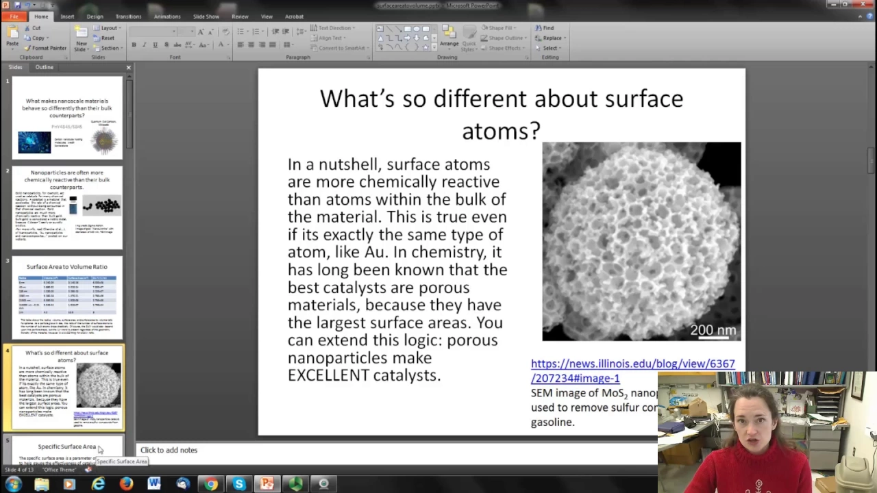
Surface area to volume ratio
2.3K
The surface area to volume ratio increases dramatically as particle size decreases. For spheres ranging from 5 nanometers to 1 meter in radius, the surface area to volume ratio changes from approximately 10^8 to just 3. This means that as particles become smaller, the proportion of atoms located at the surface relative to the total number of atoms increases substantially. The relationship follows an inverse linear pattern where smaller particles have proportionally more surface area available for interaction.
Click to watch →
Surface to Volume Ratio and Quantum Confinement by Dr. N Shankaraiah
376
As the size of a material decreases, the surface area to volume ratio increases. This can be demonstrated by dividing a 1-meter cube into smaller cubes: when divided into 8 equal parts (each 0.5m), the total surface area increases from 6m² to 12m²; when divided into 27 equal parts (each 0.333m), the surface area increases to 18m². When divided into grains with side length 0.1 nanometers, the surface area becomes approximately 2.5 square meters. This demonstrates that reducing particle size dramatically increases the surface area relative to volume.
Click to watch →
Prerequisite Knowledge
- Concept 01Basic understanding of the metric system, scientific notation, and scale of measurements (micrometer, nanometer, angstrom).
- Concept 02Fundamental concepts of atomic structure, chemical bonding, and crystal lattices from introductory physics and chemistry.
- Concept 03The geometric concept of surface-area-to-volume ratio and how it changes as particle size decreases.
Subsequent Learning
- Step 01Synthesis and fabrication methods of nanomaterials, specifically comparing top-down (lithography, milling) and bottom-up (chemical vapor deposition, self-assembly) approaches.
- Step 02Characterization techniques utilized to analyze nanostructures, such as Scanning Electron Microscopy (SEM), Transmission Electron Microscopy (TEM), and Atomic Force Microscopy (AFM).
- Step 03The study of quantum confinement effects and how material properties (optical, electrical, and magnetic) change drastically at the nanoscale.
- Step 04Practical engineering applications of nanomaterials, including the utilization of carbon nanotubes, graphene, and quantum dots in electronics and medicine.
Nano Scale
Applications
Nano Scale
0:00Playing Section
- 1
Defines nano as one billionth of a unit.
- 2
Compares nanometers with angstroms and atom sizes.
Nanotoxicology and the Precautionary Principle in Nanotechnology
While engineering lectures highlight the revolutionary optical, electrical, and mechanical properties of nanomaterials, a critical counter-perspective is found in nanotoxicology. This field argues that the very characteristics that make nanomaterials desirable—such as high surface-area-to-volume ratios and quantum effects—also render them highly reactive and potentially toxic. Nanoparticles can easily cross biological barriers, accumulate in tissues, and cause unprecedented cellular damage, yet their long-term environmental and health impacts remain largely unknown. Proponents of this perspective advocate for the Precautionary Principle, arguing that the rapid integration of nanomaterials into consumer goods and engineering applications has dangerously outpaced the development of safety regulations and toxicity testing frameworks.
Deep Dive
Synthesis and fabrication methods of nanomaterials, specifically comparing top-down (lithography, milling) and bottom-up (chemical vapor deposition, self-assembly) approaches.

Green Chemistry and Nano Chemistry Class 12th Chemistry Part 3
78.2K
Three main synthesis methods exist: (1) Top-down - breaking bulk material into smaller particles (mechanical milling, lithography); (2) Bottom-up - building from atoms/molecules (chemical vapor deposition, self-assembly); (3) Sol-gel - hydrolysis and condensation reactions forming gel networks. Each method offers different advantages for producing specific types of nanomaterials with controlled properties.
Click to watch →

Unit 5th One Shot AKTU Exam special by Lalit Rathi sir #aktu #akturesult2023 #aktuexam #oneshot
31.8K
Nanomaterial fabrication uses two main approaches: (1) Top-down approach breaks bulk materials into smaller pieces until reaching nanoscale (lithography, etching, milling), characterized by surface imperfections and material waste; (2) Bottom-up approach assembles small particles or atoms into larger nanostructures (self-assembly, chemical synthesis, atomic layer deposition), enabling precise control over structure and composition. Chemical Vapor Deposition (CVD) is a top-down method for synthesizing carbon-based nanomaterials, where carbon-containing gases react with substrates at elevated temperatures (100°C to 1000°C) to deposit thin films or nanostructures. The sol-gel process is a bottom-up technique involving transition from liquid solution (sol) to solid gel-like network through hydrolysis, condensation, aging, drying, and calcination. This enables production of nanomaterials with controlled size, shape, and composition for applications in catalysis, sensors, optical devices, and other fields requiring precise material properties.
Click to watch →

Top down approach and Bottom up approach to produce nanomaterials
144K
Nanomaterials can be produced using two fundamental approaches: the top-down approach, which involves reducing bulk materials into progressively smaller pieces through physical processes, and the bottom-up approach, which constructs nanomaterials by assembling atoms and molecules through chemical processes to form complex nanostructures.
Click to watch →

Synthesis of Nanomaterials - Top - down Vs Bottom - Up Approaches
80.3K
Nanomaterials are synthesized through two primary approaches: the top-down approach involves physically breaking down bulk materials into smaller pieces (such as slicing, milling, or grinding) until reaching the nanoscale, while the bottom-up approach constructs nanomaterials by assembling atoms or molecules into clusters through nucleation and self-assembly processes; both approaches can produce nanostructures like quantum dots, nanoparticles, nanorods, and nanotubes, but differ in starting materials (solid for top-down, liquid/gas for bottom-up), cost efficiency, and material utilization.
Click to watch →

Nano Technology | Science & Technology for RAS Prelims 2026 | English Medium | Santosh Sir
686
Nanomaterials are synthesized using two main approaches. The top-down approach (simpler, faster) breaks larger particles into nanoscale particles through physical, chemical, and mechanical methods, then deposits them as monolayers. Examples include mechanical milling, nano-lithography, laser ablation, and sputtering. The bottom-up approach (more complex, time-consuming) builds nanomaterials from atomic particles (protons, neutrons, electrons) through ionization to create free radicals that form clusters. Examples include sol-gel, spinning, CVD, pyrolysis, and biosynthesis. The bottom-up approach produces more efficient materials with designed output.
Click to watch →
Deep Dive
Characterization techniques utilized to analyze nanostructures, such as Scanning Electron Microscopy (SEM), Transmission Electron Microscopy (TEM), and Atomic Force Microscopy (AFM).

Characterization techniques for nanomaterials| SEM| TEM| AFM| Electron microscopy| Scanning Electron
3.3K
This video explains three key characterization techniques for nanomaterials: Scanning Electron Microscopy (SEM) uses an electron beam to scan specimen surfaces, detecting secondary electrons for topographical imaging with resolution up to 1 nm; Transmission Electron Microscopy (TEM) transmits electron beams through thin specimens to reveal internal structures at resolutions down to 0.1 nm; and Atomic Force Microscopy (AFM) measures atomic forces between a sharp tip and sample surface to generate 3D topographical images without requiring vacuum, making it suitable for insulating and biological samples.
Click to watch →

Nano-Chemistry ONE SHOT CSIR NET|GATE|ASSISTANT PROFESSOR|UPSC#csirnet #upsc #assistantprofessor
209
Various techniques characterize nanomaterials: (1) SEM (Scanning Electron Microscopy) - shows surface morphology, (2) TEM (Transmission Electron Microscopy) - reveals internal structure, (3) AFM (Atomic Force Microscopy) - measures surface topology and roughness, (4) XRD (X-ray Diffraction) - determines crystallographic structure, (5) FTIR - identifies chemical bonds and molecular structure, (6) Raman Spectroscopy - reveals vibrational modes and composition, (7) UV-Vis Spectroscopy - studies optical properties and band gap, (8) TGA (Thermogravimetric Analysis) - measures thermal stability, (9) Zeta Potential - determines surface charge and colloidal stability, (10) XPS (X-ray Photoelectron Spectroscopy) - analyzes surface chemical composition.
Click to watch →
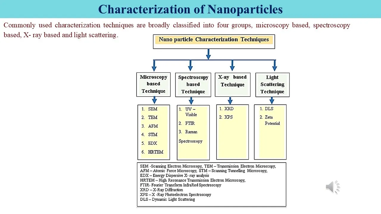
Characterization of nanoparticles.| Prof. Anita Salunkhe #nanotechnology
763
Microscopy-based techniques are essential for morphological studies of nanoparticles, determining size and shape. Scanning Electron Microscopy (SEM) uses an electron beam to scan sample surfaces, providing 3D topographical images with large depth of field. Transmission Electron Microscopy (TEM) transmits electrons through thin samples for internal structure analysis. Atomic Force Microscopy (AFM) scans surfaces with atomic-scale probes, providing accurate size/shape measurements without mathematical treatment. Scanning Tunneling Microscopy (STM) uses quantum tunneling for atomic-resolution imaging. Energy Dispersive X-ray Spectroscopy (EDX) determines elemental composition by analyzing X-rays emitted when electron beams strike samples. High Resolution TEM (HRTEM) provides atomic-level crystallographic imaging.
Click to watch →

Week 8-Lecture 49 : Surface characterization techniques
11.6K
Surface characterization techniques such as Transmission Electron Microscopy (TEM), Scanning Electron Microscopy (SEM), and Atomic Force Microscopy (AFM) are essential tools in nanoscience and nanotechnology for visualizing and analyzing materials at the atomic and molecular level, enabling researchers to study surface structures, topographies, and interfacial interactions that determine material properties and behaviors.
Click to watch →
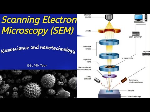
Scanning Electron Microscopy (SEM)... Nanoscience and [email protected]
1.4K
Scanning Electron Microscopy (SEM) is a powerful characterization technique for nanomaterials that uses a focused electron beam (1-50 keV) to scan across a sample surface, generating three main imaging modes: secondary electron imaging (detects low-energy electrons from surface atoms for topographical contrast), backscattered electron imaging (detects high-energy electrons scattered by atomic nuclei for compositional contrast between light and heavy elements), and elemental X-ray analysis (detects characteristic X-rays from inner-shell electron transitions for chemical composition determination); SEM requires conductive samples or metal coating (gold/iron) and provides information on nanostructure morphology, size, orientation, and elemental composition.
Click to watch →
Deep Dive
The study of quantum confinement effects and how material properties (optical, electrical, and magnetic) change drastically at the nanoscale.

Properties of Nanomaterials (Part-1) || Quantum confinement || Surface to volume ratio ||
3K
In bulk materials, atoms are closely packed with approximately 10^23 atoms per unit cell, causing energy levels to mix and form continuous valence and conduction bands. When materials are reduced to the microscopic range (10^-6 m), containing about 1,000 atoms, energy levels become moderately discontinuous. At the nano range (10^-9 m), with only 10-15 atoms, energy levels become fully discontinuous. This quantum confinement effect causes the same material to exhibit different optical, electrical, and other properties depending on its size within the 1-100 nanometer range.
Click to watch →
Nano Materials Properties: Quantum Effects & Surface Area (Ep. 4)
41K
Nanomaterials exhibit unique physical and chemical properties different from bulk materials due to two primary factors: the quantum confinement effect (where energy bands separate at the nanoscale, changing electrical and optical behavior) and the drastically altered surface-to-volume ratio (where smaller particles have proportionally more surface area available for interaction). These effects explain phenomena such as gold nanoparticles appearing violet or wine red instead of yellow, graphene being 10,000 times stronger than steel, and the ability to tune material properties through size, shape, and doping for applications in electronics, catalysis, and solar cells.
Click to watch →

Mod-01 Lec-25 Electrical, Magnetic and Optical Properties of Nanomaterials
44.7K
When semiconductor nanoparticles are reduced in size, quantum confinement effects cause the band gap energy to increase (blue shift) and the band levels to become quantized, leading to distinct optical absorption and emission properties compared to bulk materials; this is demonstrated through examples like gallium arsenide nanocrystals showing a blue shift from 1.43 eV to 2.36 eV and cadmium selenide nanoparticles exhibiting color changes from red to blue with decreasing particle size, while metallic nanoparticles show different behavior where surface plasmon resonance dominates and optical properties are less sensitive to size changes.
Click to watch →
Lecture 4 (Unit 5)|| Nano materials, Quantum dot, Quantum wires, Quantum well || Engineering Physics
206
Nanomaterials (1-100 nm) exhibit enhanced properties compared to bulk materials due to two key factors: (1) increased surface-to-volume ratio leading to higher reactivity, and (2) quantum confinement effects where reducing dimensions to the Bohr radius (0.5 Å) causes energy levels to transition from continuous to discrete, altering optical, thermal, mechanical, electrical, and magnetic properties. Based on confinement dimensions, nanomaterials are classified as quantum wells (1D confinement), quantum wires (2D confinement), or quantum dots (3D confinement), each exhibiting distinct electronic and optical behaviors.
Click to watch →

B.Tech E- Physics | Most Important Questions on Nanomaterials for Exams | Score High !
3.7K
Nanomaterials demonstrate distinctive electrical, optical, and magnetic behaviors stemming from quantum confinement effects. Electrically, the transition from continuous energy bands in bulk materials to discrete energy levels in nanomaterials causes increased conductivity in nano-ceramics and magnetic composites, with quantum confinement in semiconductors increasing effective band gaps. Optically, decreasing particle size creates discrete energy levels leading to band gap increases and blue shifts in absorption/emission spectra—gold nanoparticles become transparent at 10 nm, and further size reduction causes blue color shifts. Magnetically, nanomaterials exhibit phenomena absent in bulk: ferromagnetic particles become single-domain, superparamagnetism emerges, giant magnetoresistance appears in hybrids, and antiferromagnetic materials may behave as ferromagnets. Transition metals show superparamagnetism instead of bulk ferromagnetism, while normally paramagnetic elements like sodium, potassium, and radium exhibit ferromagnetic behavior as nanoparticles. These transformations occur because reduced dimensions cause surface atoms to dominate material behavior, fundamentally altering electronic, optical, and magnetic responses.
Click to watch →
Deep Dive
Practical engineering applications of nanomaterials, including the utilization of carbon nanotubes, graphene, and quantum dots in electronics and medicine.

Intro to #graphene | Lesson 03 | Quantum Dots & #nanotechnology Course Dr. James Tour
9.4K
Coal contains graphene-like structures formed geologically over millions of years. Research demonstrated that coal can be converted to graphene quantum dots through oxidation with nitric and sulfuric acid mixtures, with different coal types yielding different-sized dots (anthracite: 28 nm, bituminous: ~2.3 nm). These quantum dots exhibit size-dependent fluorescence for applications including product authentication, marijuana traceability, and fracking water tracing. Carbon nanotubes can be chemically split into graphene nanoribbons using potassium permanganate oxidation. Graphene nanoribbons enable transparent conductive films for touchscreens and anti-icing coatings for aerospace applications, where heated graphene coatings melt ice on glass surfaces without blocking radar signals.
Click to watch →
Nano Technology | Science & Technology for RAS Prelims 2026 | English Medium | Santosh Sir
686
Key nanomaterials include quantum dots (0D, invented by Alexei Ekimov), carbon nanotubes (1D, invented by Sumio Iijima), and graphene (2D, invented by Geim and Novoselov). Quantum dots emit different colors based on size, used in QLED TVs and cancer therapy. Carbon nanotubes are lightweight, superconducting, and 100 times stronger than steel, used in spacecraft wiring and energy storage. Graphene is 200 times stronger than steel, transparent, and highly conductive, used in batteries, solar cells, and optical devices. Dendrimers (3D branched structures) are used for targeted drug delivery, allowing a single smart medicine to deliver 25-30 different medications to different body locations efficiently.
Click to watch →

ENGINEERING CHEMISTRY LECTURE 07 ''Introduction to Nanomaterials'' By Dr. Niti Maheshwari, AKGEC
11.1K
Fullerenes (discovered 1985, Nobel Prize 1996) are carbon allotropes with truncated icosahedron structures (C60 buckyballs), produced by arc discharge between graphite rods in helium. Applications include targeting degenerative diseases, MRI contrast agents, LEDs, and electronic devices. Carbon nanotubes are cylindrical structures formed by rolling graphene sheets, existing as single-walled or multi-walled variants with conducting, semiconducting, or insulating properties depending on rolling angle. They exhibit extraordinary thermal conductivity, exceptional tensile strength, flexibility, and low thermal expansion, enabling applications in thermal management, field emission, energy storage, molecular electronics, and polymer composites. Nanowires are structures with diameters constrained to tens of nanometers where quantum effects dominate, including metallic (Ni, Pt, Au), semiconducting (silica), insulating (SiO2, TiO2), and molecular varieties (DNA). Quantum dots are three-dimensional nanomaterials with all dimensions in the nanoscale, enabling applications in chemical mechanical polishing, magnetic recording, sunscreens, MRI contrast agents, and biomagnetic separations.
Click to watch →

नैनोप्रौद्योगिकी (Nano Technology) - Chapter 10 | Science & Technology | UPSC 2025
16.1K
Scientists create nanomaterials by manipulating atomic arrangements. Carbon nanotubes are cylindrical nanostructures made of carbon atoms arranged in tube-like structures. Graphene is a single layer of carbon atoms in a honeycomb pattern, so thin that 4 million sheets would make just 1 millimeter. Both are extremely strong, flexible, and excellent electrical conductors. These materials enable applications from lightweight aircraft to flexible solar panels.
Click to watch →

NANOMATERIAIS NA ÁREA DA QUÍMICA
1.2K
Sumio Iijima synthesized carbon nanotubes in 1991—hollow cylindrical structures with nanoscale diameters but extended lengths, exhibiting exceptional electrical conductivity. Graphene, a single layer of graphite, was isolated by Geim and Novoselov in 2004 at the University of Manchester. Graphene possesses extraordinary properties: 200 times stronger than steel, one million times thinner than a human hair, highly conductive due to conjugated double bonds, and chemically inert. They received the Nobel Prize in Physics in 2010. Quantum dots, semiconductor nanoparticles discovered between 1980-1995, enable vibrant color displays through quantum confinement effects. Nature itself utilizes nanotechnology: lotus leaves have nanostructures preventing water penetration, and geckos use millions of nano-suckers for wall climbing.
Click to watch →
Nano Scale
Applications
Nano Scale
0:00- 1
Defines nano as one billionth of a unit.
- 2
Compares nanometers with angstroms and atom sizes.
Nanotoxicology and the Precautionary Principle in Nanotechnology
While engineering lectures highlight the revolutionary optical, electrical, and mechanical properties of nanomaterials, a critical counter-perspective is found in nanotoxicology. This field argues that the very characteristics that make nanomaterials desirable—such as high surface-area-to-volume ratios and quantum effects—also render them highly reactive and potentially toxic. Nanoparticles can easily cross biological barriers, accumulate in tissues, and cause unprecedented cellular damage, yet their long-term environmental and health impacts remain largely unknown. Proponents of this perspective advocate for the Precautionary Principle, arguing that the rapid integration of nanomaterials into consumer goods and engineering applications has dangerously outpaced the development of safety regulations and toxicity testing frameworks.
Basic understanding of the metric system, scientific notation, and scale of measurements (micrometer, nanometer, angstrom).
Fundamental concepts of atomic structure, chemical bonding, and crystal lattices from introductory physics and chemistry.
The geometric concept of surface-area-to-volume ratio and how it changes as particle size decreases.
Synthesis and fabrication methods of nanomaterials, specifically comparing top-down (lithography, milling) and bottom-up (chemical vapor deposition, self-assembly) approaches.
Characterization techniques utilized to analyze nanostructures, such as Scanning Electron Microscopy (SEM), Transmission Electron Microscopy (TEM), and Atomic Force Microscopy (AFM).
The study of quantum confinement effects and how material properties (optical, electrical, and magnetic) change drastically at the nanoscale.
Practical engineering applications of nanomaterials, including the utilization of carbon nanotubes, graphene, and quantum dots in electronics and medicine.
53.7K views712likes4:02@EkeedaOriginal Release: 2020-11-05
click the bell icon to get latest videos from Ikeda hello friends today we are going to learn something about nanomaterials so what are these nanomaterials we have been using this word nano for quite some time now what is something specific about this nanomaterials but before learning something specific about the nanomaterials let us first of all focus on why do we use this word nano as all of you know that the word nano corresponds to 10 raise to minus 9 of a unit that is one billionth of a unit how big is this one billion it is one followed by nine zeroes now when I say one billionth of a unit say for example unit is let us say we are taking as 1 meter 1 divided by 1 followed by 9 zeros that will correspond to 10 raised to minus 9 meters which in short we write it as 1 nano meter now let us compare this unit with a unit which we know and there is which is also as small as a nanometer and that is an angstrom all of you know that we use this and strong in measuring the dimension of atoms we also use the angstrom in measuring the dimensions of nucleus of an atom so how do I compare between angstroms and nanometers and strong as you know is 10 raise to minus 10 of a meter and nanometers that is nm in short as you have just now learned corresponds to 10 raise to minus 9 meters so 10 raise to minus 1 and strong corresponds to 1 nanometre isn't it very a small unit a very small unit here we show you a scale in nanometers so at one end you have a figure of man and at the other hand you have a depiction of an atom so the height of a man in nanometers is 10 raised to 9 nanometers and the other end the dimensions of an atom is 10 raised to minus 1 nanometers or one angstrom an intermediate between them this is for your comparison we have various particles as well as living objects that corresponds in the nanometer scale so any material which has particles in the nanometer scale is known as nano material and a study of this of their behavior is called as nano science and if we want to fabricate something in this scale of particles then we say that it is called as a nano technology thanks for watching this video dear students please subscribe to our channel Ikeda
Up Next
16:50
Top-Down Nanofabrication: Ball Milling, Lithography & Etching
@STEMwithDrTiwari
2.3K views•2025-10-13

48:00
Clean Water, Green Concrete & Nickel from Plants: Sustainable Inventions Explained
@business
94.3K views•2025-11-06

30:43
8259 Programmable Interrupt Controller | Features & Applications
@Ekeeda
29.4K views•2018-08-11

33:39
How a Student's Question Saved a NYC Skyscraper from Collapse
@veritasium
22.8M views•2025-04-26
Related Study Plans & Knowledge Roadmaps
Structured learning paths in Engineering
engineering
Building Acoustic Levitators: Physics & Arduino
01The Physics of Sound and Standing Waves
02Piezoelectric Transducers and H-Bridge Drivers
03Arduino Programming: Generating 40 kHz Signals
+ 2 more learning modules
14h5 modules
Explore Roadmap
engineering
Building Peltier Cloud Chambers: Particle Tracks
01Cosmic Rays & Cloud Chamber Physics
02Thermoelectric Cooling (TEC) Fundamentals
03Custom Liquid-Cooling Loop Design
+ 2 more learning modules
18h5 modules
Explore Roadmap
engineering
Yagi-Uda Antennas: Modeling, Build & VNA Test
01Introduction to RF and Antenna Fundamentals
02Yagi-Uda Antenna Design Principles
03Antenna Modeling and Simulation in 4NEC2
+ 2 more learning modules
18h5 modules
Explore Roadmap
engineering
ECG Monitor Design: Op-Amps, Filters & Noise
01Electronics & Breadboard Basics
02Op-Amps and Instrumentation Amplifiers
03Bioelectricity and ECG Fundamentals
+ 2 more learning modules
18h5 modules
Explore Roadmap