
















![[함께배우기] 127일차, 반도체 배우기, HBM과 함께 항해하는 3명의 선원(테크윙, 오로스테크놀로지, 엘티씨)](https://i.ytimg.com/vi/MssFfYOYcRU/maxresdefault.jpg)



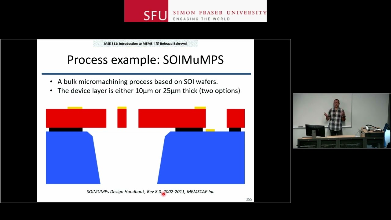
![[MEMS 응용 기술 이야기 #1] 반도체와 MEMS 비교: 차이점과 융합의 미래](https://i.ytimg.com/vi_webp/S_-I6G7G9Fk/maxresdefault.webp)



Top-down nanofabrication transforms bulk materials into nanoscale structures through mechanical reduction and pattern-based techniques; ball milling uses high-energy collisions to refine grain sizes to 5-100 nm by inducing severe plastic deformation and dislocation multiplication, while lithography (including photolithography, electron-beam lithography, and ion-beam lithography) defines nanoscale patterns with resolutions from 13.5 nm to sub-10 nm, followed by etching (wet or dry) that transfers these patterns into functional materials with precise spatial control essential for creating transistors, sensors, and nanophotonic devices.
Top-Down Nanofabrication: Ball Milling, Lithography & Etching
Added:Understanding of the nanoscale, including scale dimensions (1-100 nm) and how material properties change at this level.
The conceptual distinction between top-down and bottom-up approaches in nanotechnology.
Basic principles of optics and wave-particle duality, particularly how light is used to transfer patterns in manufacturing.
Fundamental chemistry of materials, including solid-state properties, polymers (photoresists), and basic chemical reactions.
Advanced lithography techniques, such as Electron-Beam Lithography (EBL), Extreme Ultraviolet (EUV) lithography, and Nanoimprint Lithography.
High-precision etching methodologies, including Deep Reactive-Ion Etching (DRIE) and Atomic Layer Etching (ALE).
Characterization tools used to verify nanofabricated structures, such as Scanning Electron Microscopy (SEM) and Atomic Force Microscopy (AFM).
Real-world integration of these processes in semiconductor manufacturing, microelectromechanical systems (MEMS), and quantum computing hardware.
2.3K views6likes16:50Original Release: 2025-10-13
Welcome back to our lecture series on nanoructured materials science and technology. I am professor Ashtoh Diwari from the department of material science and engineering at the University of Utah. In the previous lecture we studied crystalgraphy and draction understanding how atomic planes and reciprocal latises determine material properties. Today we shift from analyzing nanoructures to creating them. This lecture introduces nanop fabrication focusing on approaches that deliberately shape matter at the nanometer scale. We will explore why nanop fabrication is central to modern technology and examine several representative methods mechanical pattern based and chemical used to form nanoscale features.
Nanop fabrication bridges the gap between nanocience and nanotechnology.
It provides the means to turn theoretical ideas about atomic scale behavior into tangible structures such as transistors, sensors, catalysts, and nanomechanical systems. For any nanom scale device to function, its components must be fabricated with precise spatial control, often below 100 nanometers.
Achieving this control requires specialized tools and strategies that can manipulate or shape materials with atomic level accuracy. In the next few slides, we will classify these methods and then explore in detail the top-down category of fabrication techniques.
Nanop fabrication methods fall broadly into two categories. In the top-down approach, we begin with bulk material and reduce it to the nano scale by removal, patterning or shaping. Examples include ball milling, lithography, and etching. In contrast, the bottom up approach assembles atoms and molecules into larger structures through processes such as solid gel synthesis, chemical vapor deposition, electroplating, and self assembly. Both approaches complement each other. Top down ensures precision and pattern fidelity while bottom up offers atomic control and scalability from the smallest building blocks. This lecture focuses on the top down family. One of the earliest and most practical top-down nanop fabrication methods is high energy ball milling. The principle is straightforward. Powders and hardened balls are sealed into a rotating drum.
As the drum turns, collisions between balls and powder particles generate intense impact and friction. These repeated collisions cause severe plastic deformation progressively refining grain size into the nanometer range, typically 5 to 100 nanometer. Bore milling is versatile and cost effective. It can process metals such as aluminum and copper alloys including steels and high entropy systems, ceramics like jironia and even metal matrix composits. Because of its scalability and simplicity, it is used extensively in both laboratories and industrial production.
The driving mechanism of ball billing is the alternating sequence of impact and friction. Each collision transmits kinetic energy to the powder trapped between the balls. During impact, particles fracture producing a smaller fragments. During relaxation, some cold w also forming new interfaces.
This continuous cycle of fracture and welding refineses the grains step by step. Dislocations and strain accumulate and eventually nanoristalline structures with extremely high defect densities emerge responsible for enhanced hardness strength and reactivity.
Different mill designs achieve similar goals through distinct motion paths. A planetary mill has jars rotating on their own axis while orbiting a central axis producing very high energy and shear ideal for small batches and alloying research. An attriator mill uses a stationary vertical tank with a rotating steer shaft enabling continuous operation and larger batch sizes. Well suited to industrial nano composits, a shaker mill rapidly oscillates a while, giving moderate energy and small batch capacity. Useful for quick laboratory tests or a mechanochemical reactions.
Each configuration balances energy input, throughput, and scalability depending on the intended application.
Several parameters govern the efficiency of ball milling. Milling time. Longer duration yield finer grains but risk contamination.
Rotational speed or energy input. Higher speeds increase collision frequency and energy transfer. Ball to powder ratio. A higher ratio accelerates refinement yet may promote elomeration.
Atmosphere. Inner gases such as argan or nitrogen prevent oxidation while reactive gases can initiate compound formation. By tuning these variables, researchers can tailor micro structure, composition, and phase evolution to achieve desired properties.
At the atomic scale, ball milling induces severe plastic deformation.
Dislocation multiplication subdivides grains into nanosized domains while restored strain energy may stabilize metastable or amorphous faces. As a result, we can obtain nano crystalline metals, alloys, ceramics and composite powders exhibiting enhanced mechanical strength, magnetic behavior or catalytic activity. Nevertheless, challenges remain. contamination from the milling media, broad particle size distribution and difficulty in achieving large scale uniformity.
Understanding these tradeoffs helps select optimal milling conditions for each material system.
So far we have discussed a mechanical route for producing nanoized powders.
Let us now turn to pattern based nanop fabrication where we create nanoscale features directly on solid surfaces.
Unlike ball milling which refineses particles in bulk, these methods produce precise repeatable patterns used in integrated circuits, sensors and photonic devices. The most prominent patterning technique is lithography followed by etching which transfers those patterns into functional material.
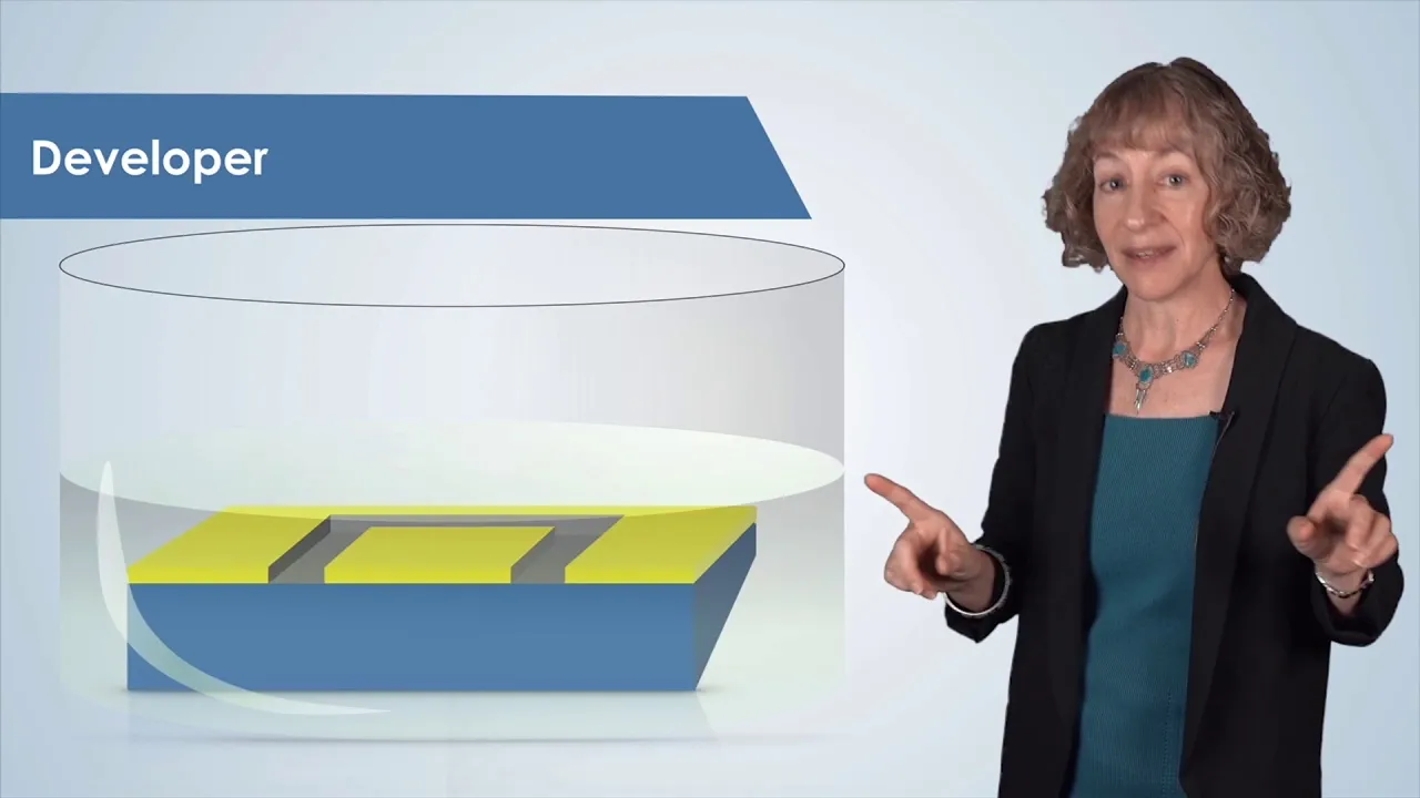
Lithography aims to define nanoscale patterns with high spatial precision. A typical process cycle includes substrate preparation and resist coating exposure to a beam of light or any other radiation development to reveal the pattern regions.
Etching to transfer the pattern into the substrate and resist removal for a clean surface. This quote expose develop edge clean sequence underpins nearly every semiconductor and M's fabrication workflow. Lithography thus translates digital design data into tangible nanoructures.
Photo lithography is the foundation of modern semiconductor manufacturing. A light source projects ultraviolet radiation through a patterned mask onto a photo resist coated wafer. The transparent and opaque regions of the mask determine which parts of the regist are exposed. In positive resists, exposed reasons dissolve away. In negative resists, exposed reasons cross link and remain. Resolution depends on the wavelength lambda and the numerical aperture of the optics with an approximate limit of lambda by 2 * na.
To achieve a smaller features, industry has evolved from near UV 365 nanometer to deep UV 248 nanometer and 193 nanome.
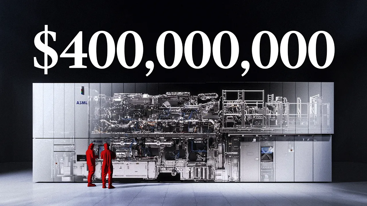
Immersion lithography and currently extreme UV 13.5 nanome. Photo lithography offers high throughput and wafer scale precision but demands costly optics, masks and alignment systems.
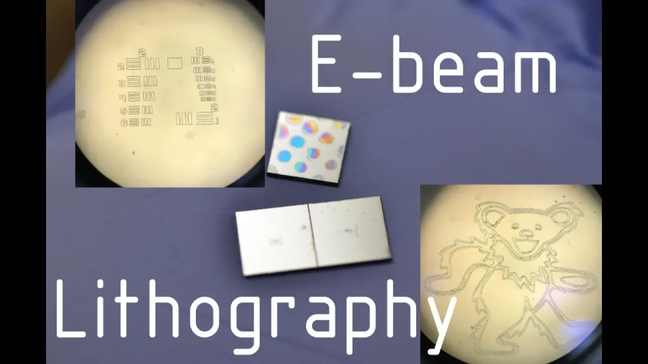
Electron beam lithography eliminates masks altogether. You finally focus electron beam scans across an electron sensitive regist according to a computerenerated pattern because electron wavelengths at t of kilo electron volts are extremely small. EPL achieves sub 10 nanometer resolution making it invaluable for quantum devices, nanowires and nanopotonic components. The flexibility of design allows any arbitrary geometry. However, EBL is slow and expensive since it writes point by point limiting its use to research and low volume prototyping rather than mass production.
Ion beam lithography operates on similar principles as EBM but uses ions instead of electrons. Because ions are far heavier, their deep broadly wavelength is much shorter than that of electrons which means in principle they can be focused into finer spots achieving even higher theoretical resolution sometimes below 10 nanometers. However, in practice, both ion and electron beam lithography reach compat comparable sub 10 nanometer resolution since the limiting factors are resist chemistry, beam interactions and system stability rather than a wavelength alone. The main distinction lies in the interaction with the substrate. Ions being massive deliver more momentum and energy which can cause implantation and surface damage. Thus, while iron beam disography potentially offers higher precision, it trades off with slower speed and greater substrate impact making it primarily a research or a collection tool rather than a high throughput fabrication method.
After pattern definition, etching transfers those patterns into the underlying material. Etching selectively removes exposed regions while protected areas remain intact. Two main categories exist. Wet etching using liquid chemical solutions and dry etching using plasmas or energetic ions. The critical attributes are selectivity preferentially removing one material over another and directionality controlling whether the process is isotropic or anisotropic.
Wet etching is generally isotropic while dry etching can achieve vertical well-defined side walls essential for nanocale electronics.
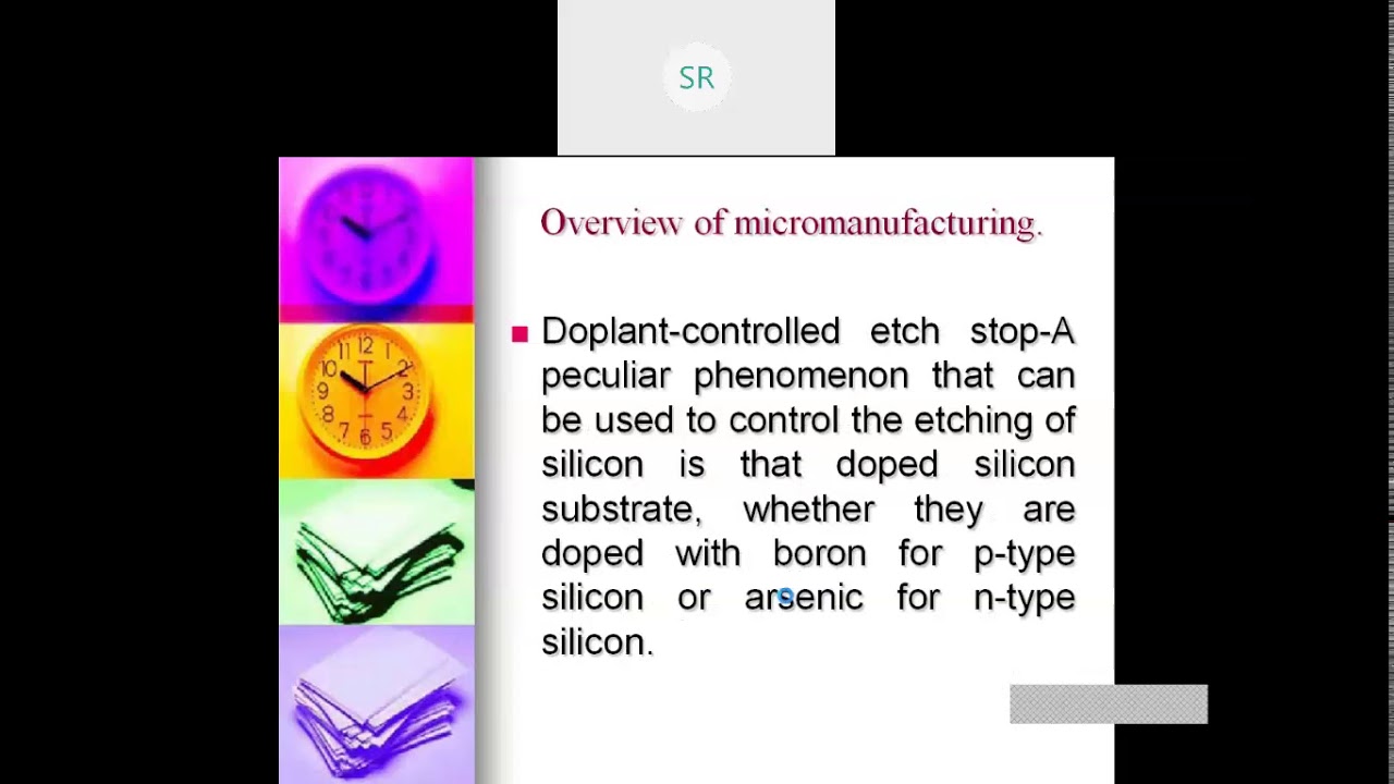
In wet etching, the wafer is immersed in a liquid chemical agent that reacts with exposed material to dissolve it into solution. Because the reaction proceeds equally in all directions, the resulting profile is rounded and may undercut the resisting is simple, inexpensive and offers high removal rates useful for many macro or microscopic uh steps. Common examples include hydrofuloric acid for SiO2, KO or TMAH for silicon and acid mixtures such as nitric acid or aquaresia for metals. Its limitations are poor directionality and limited control making it unsuitable for features that require sharp vertical edges.
Dry etching uses plasmas and iron bombardment to achieve an isotropic controllable profiles. In plasma etching, reactive neutral species chemically attack the surface. In reactive ion, ions are accelerated toward the wafer by an electric field, physically sputtering atoms and assisting chemical reactions at the surface. Variants such as jeepie also known as bosched process create high aspect ratio trenches while inductively coupled plasma riie allows higher plasma densities and precise depth control. Dry edging provides the resolution and verticality needed for integrated circuits, MEMS and nanopotonic structures through though it involves high equipment cost and potential ion induced damage.
To highlight the comparison, wet etching is a chemical process that removes material isotropically equally in all directions. It is simple, fast and inexpensive making it ideal for large area processing where extreme precision is not essential. Dry etching particularly reactive ion relies on energetic ions and reactive species to achieve anisotropic profiles with vertical side walls. This directional control allows for the definition of extremely fine patterns at the nano scale. When combined with lithography, etching techniques enable the fabrication of MEMS and NMS components, semiconductor transistors, metal interconnects and nanoructured optical or catalytic surfaces. Together, these processes provide the precision required to sculpt materials at nanometer dimensions forming the complex architectures that underpaint today's advanced technologies.
In this lecture, we explored how top-down nanop fabrication transforms bulk materials into nanoscale structures through removal and patterning. Ball milling provides a mechanical route to produce nanoristalline powders.
Lithography defines patterns with nanometer precision and etching transfers those patterns into functional materials.
Each method serves the same overarching goal precise control of matter at extremely small dimensions. In the next lecture, we will examine bottomup nanop fabrication where atoms and molecules assemble spontaneously into order nanoructures completing our view of how nanoscale materials are both formed and controlled.
Up Next

78:26
Surface Plasmon Resonance in Nanomanufacturing | Lecture 11
@mechanosynthesis
70.5K views•2012-01-26

48:00
Clean Water, Green Concrete & Nickel from Plants: Sustainable Inventions Explained
@business
94.3K views•2025-11-06
54:16
Polymer Environmental Degradation: Mechanisms & Stabilization
@iit
1.8K views•2012-07-10
33:39
How a Student's Question Saved a NYC Skyscraper from Collapse
@veritasium
22.8M views•2025-04-26
Related Study Plans & Knowledge Roadmaps
Structured learning paths in Engineering
engineering
Building Acoustic Levitators: Physics & Arduino
01The Physics of Sound and Standing Waves
02Piezoelectric Transducers and H-Bridge Drivers
03Arduino Programming: Generating 40 kHz Signals
+ 2 more learning modules
14h5 modules
Explore Roadmap
engineering
Building Peltier Cloud Chambers: Particle Tracks
01Cosmic Rays & Cloud Chamber Physics
02Thermoelectric Cooling (TEC) Fundamentals
03Custom Liquid-Cooling Loop Design
+ 2 more learning modules
18h5 modules
Explore Roadmap
engineering
Yagi-Uda Antennas: Modeling, Build & VNA Test
01Introduction to RF and Antenna Fundamentals
02Yagi-Uda Antenna Design Principles
03Antenna Modeling and Simulation in 4NEC2
+ 2 more learning modules
18h5 modules
Explore Roadmap
engineering
ECG Monitor Design: Op-Amps, Filters & Noise
01Electronics & Breadboard Basics
02Op-Amps and Instrumentation Amplifiers
03Bioelectricity and ECG Fundamentals
+ 2 more learning modules
18h5 modules
Explore Roadmap