



























In KiCad 7.0, design constraints such as minimum clearance (0.15mm), track width (0.15mm), connection width, hole size (0.3mm), via size (0.5mm), and annular clearance (0.1mm) must be configured in the board setup to ensure manufacturability; track widths can be calculated using KiCad's built-in calculator tool based on current requirements and copper thickness (typically 35 micrometers for outer layers), and net classes can be assigned to connections using the net class directive tool to automatically apply different trace widths (e.g., 0.3mm for signals and 0.5mm for power) across the entire circuit.
KiCad 7 Tutorial: PCB Constraints, Net Classes & Directive Tool
Added:Basic proficiency with the KiCad 7 user interface, including schematic capture and basic PCB layout workflows.
Fundamental concepts of PCB geometry, such as traces, vias, clearance, and copper layers.
Basic electrical theory regarding current capacity, voltage drop, and how physical trace width affects thermal performance and resistance.
An understanding of netlists and how schematic symbols map to physical footprints and connections.
Advanced high-speed PCB routing constraints, such as differential pairs, length matching, and propagation delay tuning.
Writing and utilizing custom Design Rule Check (DRC) code in KiCad for complex, multi-layer board designs.
Design for Manufacturing (DFM) principles, aligning KiCad constraints with fabrication capabilities of commercial PCB manufacturers.
Signal integrity and electromagnetic compatibility (EMC) optimization strategies using controlled impedance traces.
68.9K views993likes12:16Original Release: 2023-03-13
In this video, we'll start with adding some design constraint to the PCB layout editor, so we don't design something that's very expensive or very difficult to manufacture in a fabrication plant.
For this, we'll go to the board setup and then click on constraints. Here we need to fill in the values that a fabrication plant can handle. So, anytime we go above this threshold value, Kicad will warn us and try to keep our design within the manufacturing limit. Usually all fabrication plant will provide a capability list which we can use to fill in this data. If you're just getting started and not sure which fabrication plan to choose, we have a whole section of articles dedicated to that.
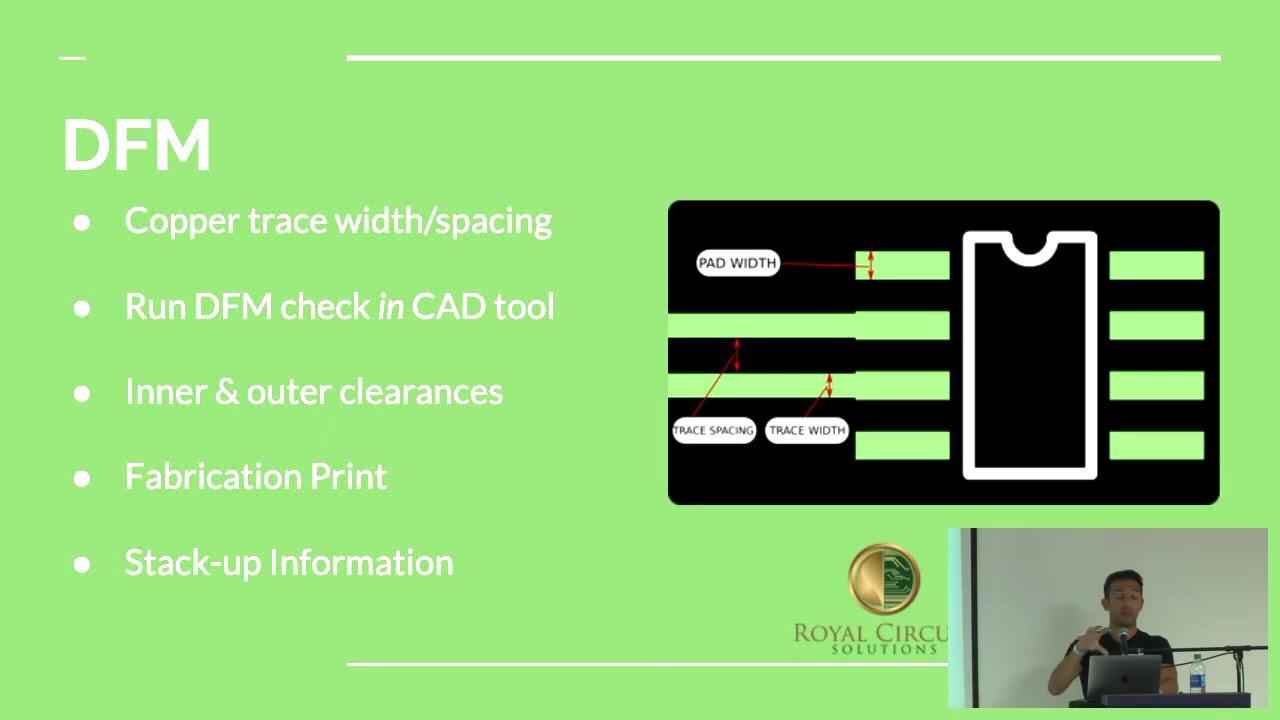
For now, I'll use this capability list, because most of the manufacturers can handle these values very easily. In Kicad, we have these default constraints, let me quickly explain what and why we have these constraints using some examples. First we have the minimum clearance, This would be the minimum distance between 2 tracks and when we go below this value we might see some weird artifacts or shorting of the tracks. This is because of the process called etching which is done during the production. To avoid this we can always design the board a little above the fabrications capable value to be on the safer side. So in this case, the capable value is 0.1 mm but 0.15 is a good value and also is recommended by the fabrication plant, so we'll go with that.
Then we have the minimum track width, which is basically the thickness of the track and similar to the previous value, this thickness is greatly affected by the etching process, if it's anything below the threshold value, the tracks might cause open circuits in the PCB. And according to the capabilities list it is 0.15 mm.
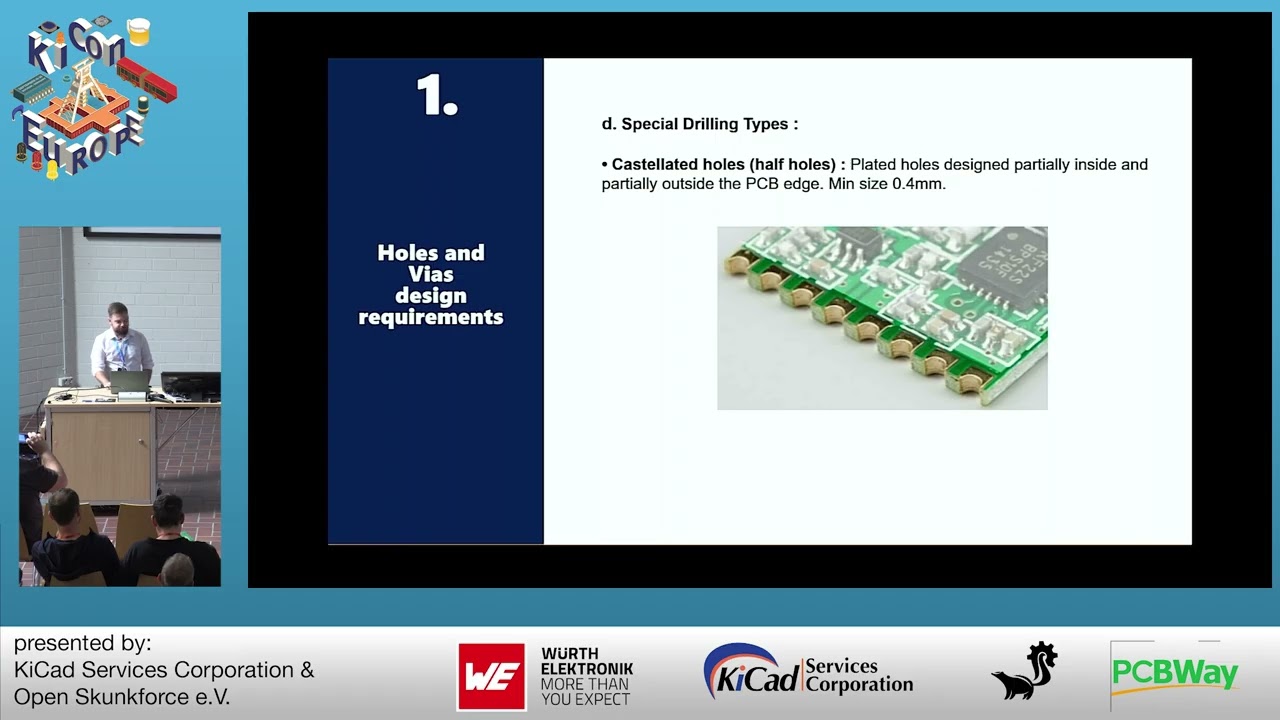
Then we have minimum connection width which is similar to the track width but this is the connection between 2 components or connection between a component and a track. Similar to the track width, if it's less than the threshold value the PCB etching process might break the connection, so we'll enter the similar value. Then we have the minimum hole size, In this case it's 0.3 mm. You can go well below this value but it would make the PCB very expensive as they have to use different process to make the hole instead of just using a drill bit.
Next we have the via size of 0.5 mm and the annular clearance is 0.1 mm.
Sorry for throwing random words at you, but the video would get longer and longer if I explain each one of them. To solve this we have created a cheatsheet of all the terminologies into a single page which you can always refer to when you don't understand these terminologies.
So I entered those values over here, 0.3, 0.5 and 0.1 mm. Finally we have 2 more clearance values, minimum track distance and minimum track distance between the edge of the PCB. The first value will help in making sure we don't take the tracks too close to the holes, so the tracks won't be damaged while drilling during production.
Similarly the second value will help in making sure we don't take the tracks too close to the edge of the board so it won't be damaged or chipped off during the final stage of production.
The hole to hole clearance just makes sense you can't have two holes close to each other during drilling so they don't form a single slot instead of two different holes.
Then we have Micro Vias, these are very little to advance for the current circuit that we are working on, so we just skip this and go to the Silkscreen. Here most of the terminologies are self-explanatory. So I'll just take the values from the capability list and just enter them over there.
We'll come back to these values when we are doing Zone filling at the end of PCB design.
Then we have length tuning which we can just keep it checked. Next we have predefined sizes.
Let's predefine some track width which we can use in the circuits, it's very similar to how we choose a wire to make the connection based on the current rating of the circuit.
For this circuit we are working, we'll just need 2 different sizes, one for signals and the other one for power tracks. To calculate this, we can use the calculator that's within Kicad.
Just go to the Kicad project window and click on calculator tools.
Then click on track width. If you like to know how the calculation is done you can see the formula is given here with some explanation. Since our circuit is very simple we can just enter the maximum current it would carry during operation. I'll just enter 1A for now.
I know the circuit we built in the previous videos won't even be close to 0.5 A but decreasing the current consumption decreases the track width which will make the track width less than our clearance value that we just set a while ago. Then for the temperature rise and trace length I'll just let them be default. As our circuit is simple and small these factors won't affect much.
Then finally there is one more factor to include, that is the trace thickness and for this value we have to pull up the capability list again. And if you look at outer layer copper thickness, we have 35 micrometer, 70 micrometer and 105 micrometer. In our case, we'll just go with 35 micrometer which is also the default setting on Kicad.
Now based on the information we gave Kicad, it gives the track width of 0.3 mm which will include in the predefined sizes. There is also something called as Internal Layer Traces, these values we can consider when we are trying to build a multi-layer PCB, so this won't be much of help now.
Since now we know the track width, I'll create a 0.3 mm track width for signal and additionally I'll create a 0.5 mm track width for power. I'm doing this just to show the difference between power and signal tracks, but theoretically 0.3mm would be good for signal and power in our circuit.
Then we have Net Classes, if you remember from our fourth video about schematics and adding net labels, we discussed how we can give name to few connections for easier understanding. Similarly we can use Net classes and create a group of connections that will share similar properties.
For example we can create 2 net classes one for signal and other for power. Now using these two classes, we can assign the thickness to the traces automatically, Instead of using the predefined sizes each time you switch between power and signal tracks.
So far we have just created the classes but never really assigned the classes to the connections that we made in the schematics. We can do this in two ways, we can either do the assignment here on both setup or we can do the same on the schematic setup. Personally I would prefer using the schematic setup. So let me close this. So let me open the schematic editor. Now if you click on any connection and see the bottom status bar, you can see we have the connection name but the net class is set to default. But in our case we want to change this to signal.
We can do this in multiple ways but the easiest way would be just do a right click on the connection and click on assign net class and under this the current name is set to slash LDR.
This is just the net label that we assigned and here we can set what kind of net class we need to assign for this connection. In this case we'll set it to signal and click on OK.
Now if I click on the same connection again, you can see the net class is set to signal. Now if I click on any connections that's related to LDR, you can see the net class is automatically set to signal. We can either do this process for all the connections or we can go to the schematic setup and here we can just enter the name of the connection and Kicad will try to automatically assign the net classes for these labels. So let me do that for MIC and set it to signal and similarly let me do it for LED and signal. Then we have ground, that'll be the power.
Then we have plus 3.3 V that will be power as well. Now there is a slight bit of a problem here. We have assigned the net classes only to the connections that have names but what about the ones that's unlabeled? For example, this connection which has the default connection name net d1k and net class is default. Since they are unlabeled there is no way to search for the pattern without a name that we manually assigned. So how about we manually try to assign.
Seems like we can't assign the net to this connection without adding a net label.
We can fix this quickly by adding a net label, but this process would become very difficult when we are trying to make a complicated circuit.
In Kicad 7, we can solve this by using net class derivative tool to assign net classes to unlabeled connections. Click on the icon here, add in a class derivative label. On this menu select the net class that we want to assign to the connection. In our case it's the signal. We can use the below settings to show how they appear on the schematic diagram. In my case, I'll keep it very simple select the dot and also I'll cut down the length by half and then hit OK, and now we'll place it on the connections.
And personally I don't like the names that's sticking out so I'll click the net class label and press the letter E and under here you have the option called show and I'll just uncheck this and click on OK. Now with this when we click back on the connection we can see on the status bar that the net class has been assigned to this connection. Now I explain how to assign the class name for labeled and unlabeled connections, let me quickly do that for the whole circuit.
Now I have assigned all the net classes. To just make sure the schematic editor is reflecting all the changes to the PCB editor, I'll close this and open the PCB layout editor.
And here I'll open the board setup, and here we can verify both setup net classes and the schematic setup net classes match up.
I know this is an insane amount of work for a very simple circuit but you need to trust the process. These settings will really help a lot in making a very good PCB at the first try.
I keep using these sentences from the past two videos that will be bringing the footprints that we assigned into the PCB layout editor but so far we took so much time just talking about the constraints, PC layout editor and so many other things but in the next video we'll make sure we get all the footprints into the PCB layout editor and we'll finally start working on our first PCB.
And we really appreciate any doubts or questions related to the topic that we are making and we are always thrilled to answer each one of your questions but please try to consider PCB Cupid QnA for a few of the questions, all you have to do is just a one-click login and ask your questions.
It'll really help us in producing more videos frequently also it will help many users who are just getting started with Kicad. So until next video, keep learning and keep creating.
Up Next

4:12
KiCad Production File Export: Gerber, Drill, and PDF Tutorial
@ProtoexpressPCB
394 views•2025-11-03

12:54
Triumph of Orthodoxy Icon: Byzantine Art & History Explained
@BenCallan
2.1K views•2024-08-06

9:49
FastAPI vs Flask vs Django: Choosing the Right Python Web Framework
@TechWithTim
302.5K views•2024-05-26

1:42
Game of Thrones Opening Credits: A Cinematic Analysis
@gameofthrones
46.3M views•2011-04-18
Related Study Plans & Knowledge Roadmaps
Structured learning paths in General & Interdisciplinary Studies
general-studies
Elevator Engineering: History, Physics & Cities
01From Hoists to Safety Brakes: The Dawn of Vertical Lift
02Hydraulic vs. Traction: The Engineering Physics of Elevators
03Modern Speed, Safety, and Algorithms
+ 2 more learning modules
12h5 modules
Explore Roadmap
general-studies
Rubber: Material Science, History & Geopolitics
01Origins of Natural Rubber & Mesoamerican History
02The Chemistry of Natural Rubber & Vulcanization
03The Geopolitics of the Rubber Boom & Colonization
+ 2 more learning modules
12h5 modules
Explore Roadmap
general-studies
Containerization: Evolution, Logistics & Trade
01Ancient Trade & Bulk Cargo: Amphorae to Barrels
02The Industrial Revolution & Cardboard Packaging
03The Containerization Revolution: Malcom McLean
+ 2 more learning modules
12h5 modules
Explore Roadmap
general-studies
Textile Tech: Evolution, Labor & Global Impact
01Pre-Industrial Textiles: Handloom & Cottage Industry
02Mechanization: The Spinning Jenny to the Power Loom
03The Factory System & Global Labor Transformation
+ 2 more learning modules
10h5 modules
Explore Roadmap