


























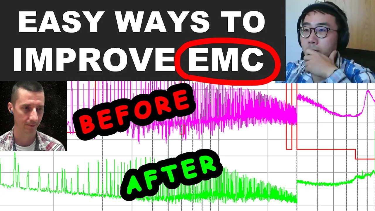

PCB layout should prioritize minimizing loop areas for high di/dt (rate of current change) currents, as these create time-varying magnetic fields that induce unwanted voltages in nearby traces through self-inductance (E = -L di/dt) and mutual inductance (E = -M di/dt); the right-hand screw rule helps determine magnetic field direction, and routing return currents directly under forward currents on adjacent layers minimizes loop area and cancels magnetic fields, making high-frequency switching circuits more critical to optimize than DC circuits.
PCB Layout Fundamentals: Mastering Noise Coupling and Loop Minimization
Added:Fundamental electromagnetic theory, specifically Faraday's Law of Induction and Lenz's Law, to understand how changing magnetic fields induce voltages.
Basic electric circuit theory, including Kirchhoff's Current Law (KCL) and the concept of current return paths in closed loops.
An understanding of basic PCB terminology and structural elements, such as traces, vias, ground planes, and multi-layer stack-ups.
Familiarity with Switch-Mode Power Supply (SMPS) operating principles, specifically high-frequency switching nodes and rapid current changes (di/dt).
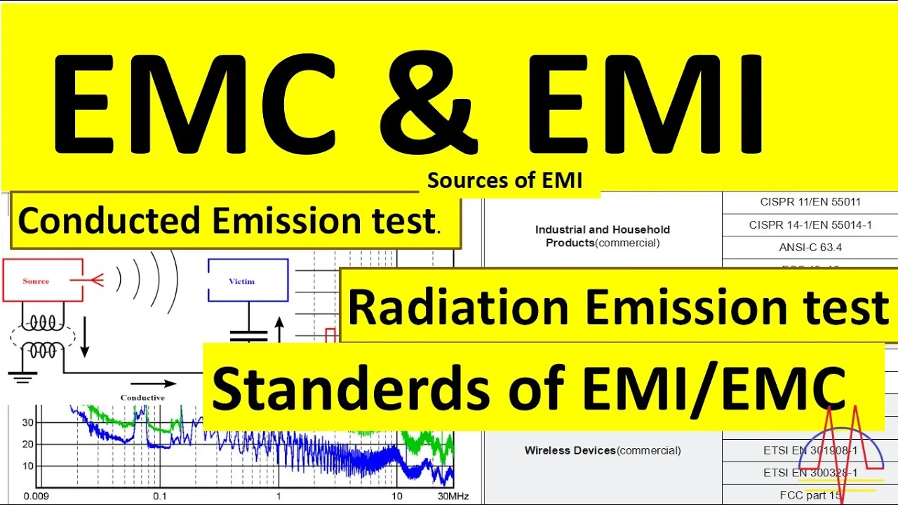
Electromagnetic Compatibility (EMC) and Electromagnetic Interference (EMI) compliance testing standards (e.g., FCC, CISPR) and mitigation strategies.
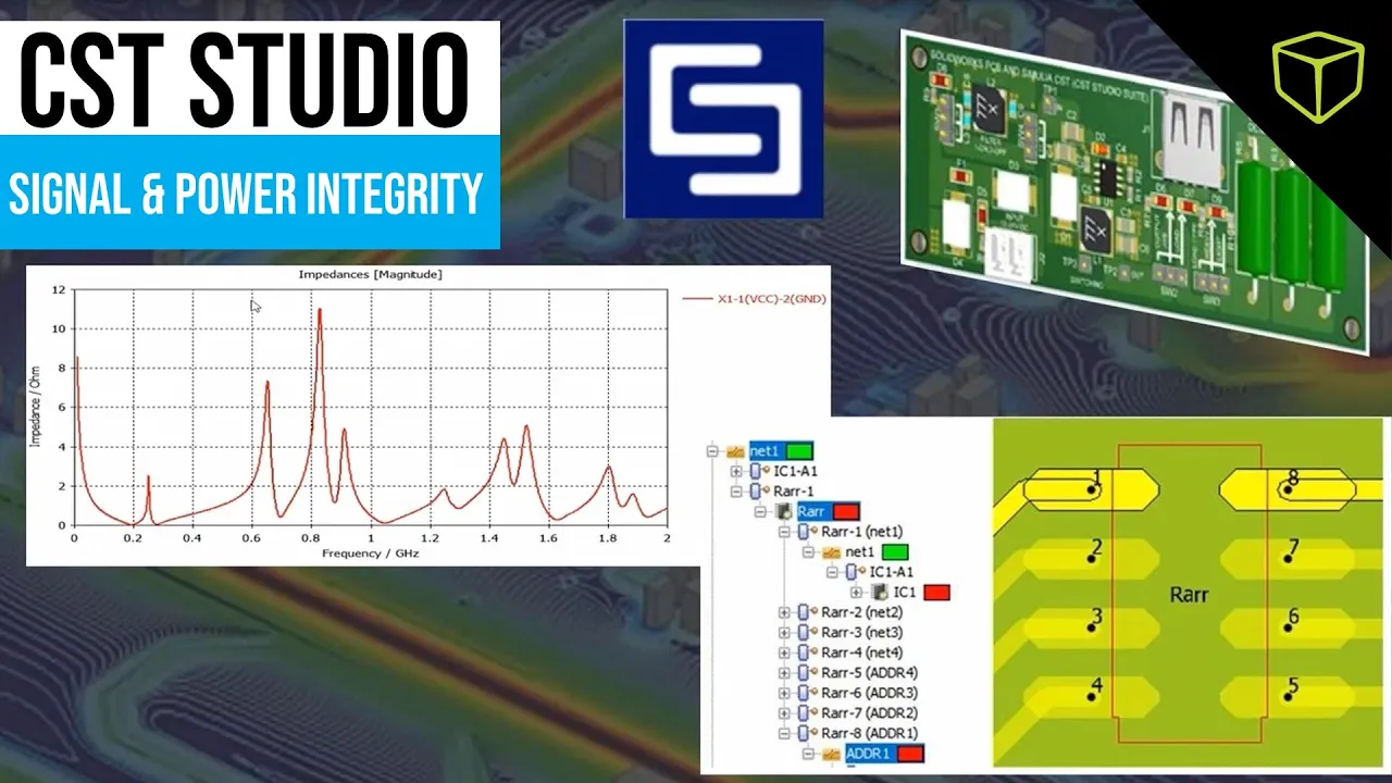
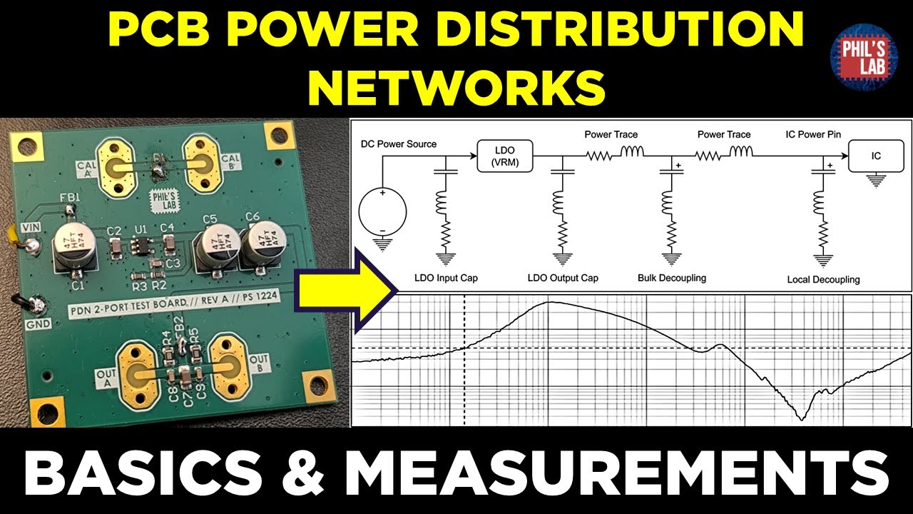
Advanced Power Integrity (PI) analysis, including decoupling capacitor optimization, target impedance, and PDN (Power Delivery Network) design.
Hands-on simulation of PCB parasitic inductance and capacitance using EDA/FEA tools like Ansys SIwave, Altium PDN Analyzer, or HyperLynx.
Practical design of active and passive EMI filters, such as common-mode chokes, differential-mode filters, and shielding enclosures.
50.5K views1.6Klikes42:38Original Release: 2021-03-17
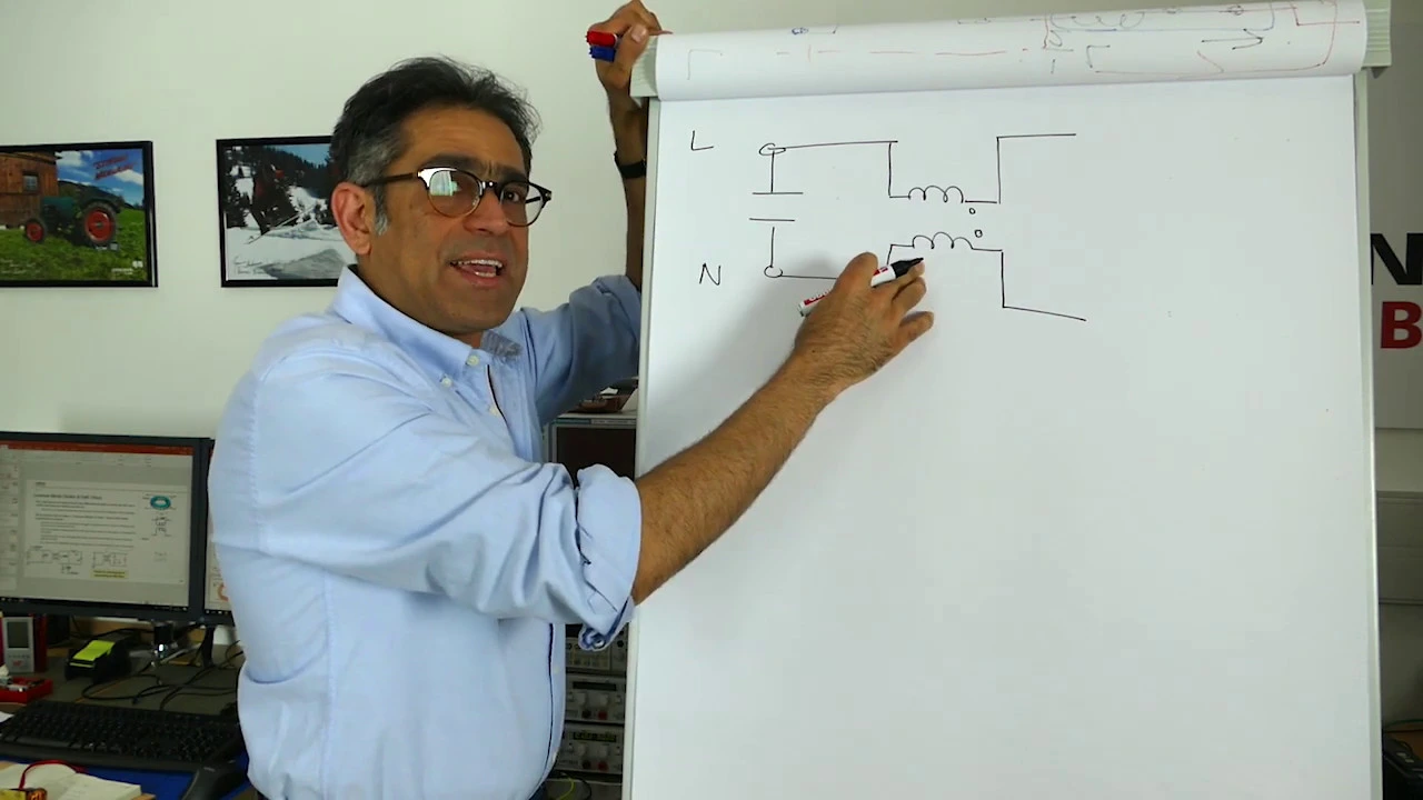
okay hi everybody uh my name is alex chesevar uh i uh um i'm delighted to be here today uh in particular because this is the first time that i've had to wear a shirt since last march i haven't been allowed out of the house for a year now so uh it's good to be able to present to some people today we're going to talk about pcb layout fundamentals uh there are a great deal of guidelines and so on on the internet about pcb layout but it is very difficult to um apply these beyond the circuit that they're describing in an application note if you don't follow the actual fundamentals and today we're just going to talk about how to deal with fast changing currents mainly because we've only got 15 minutes okay so a quick introduction there are many many tips and guidelines and so on for correct pcb layout on the internet the problem is that often these guidelines conflict with each other and they can be sometimes even contradictory many times the guidelines are either vague or ambiguous exactly how many millimeters is as close as possible to avoid jitter exactly how far away is as far as possible to avoid crosstalk if you have to avoid jitter and crosstalk but it is as close as possible and as far as possible at the same time uh i'm going to talk about currents in particular today in particular the ones in power supplies and many times you read that we have to minimize all the loop areas i mean how can we do that at the same time you cannot have zero space if you minimize absolutely everything it's not physically possible now none of these guidelines are incorrect in fact all of them are correct it's just that we need to decide when to give priority to each guideline which one is the more important one at the point of the layout that we are going to be laying out now thankfully often all we need is to apply some high school physics so we just need to know some high school physics fundamentals which we've all studied at school but it's just that we haven't applied it to pcb layout so in this webinar we will first talk about some fundamentals that you need to correctly root fast changing current traces by that i mean current traces that have got very high di dt the rate of change of current then after we talk about this high school physics stuff then we apply these fundamentals to a real life circuit and remove some of the ambiguity surrounding the pcb layout so that we see okay which one of these loops i minimized i cannot minimize all of them which one is the one that is going to give me the biggest headache and i'm going to prioritize that one in order to uh um you know in order to get a better pcb layout so first a quick reminder of high school physics rule one right hand screw rule you would have uh uh done this at the school at some point uh so and it basically says when a current flows in a conductor or a cable or a pcb track a magnetic field is formed around it it becomes magnetic we will represent this with what we call magnetic field lines the right hand screw rule allows us to determine the direction of these field lines now the direction of these field lines is important because depending on how you lay out your pcb you can either laid out in a way that these magnetic fields lines cancelling cancel each other or they reinforce each other for example if you want to build an inductor you want this magnetic field lines to reinforce each other if you want to have a quiet pcb track we usually would like these magnetic field lines to cancel each other and we'll talk about this a little bit later if you hold your current carrying conductor this is the right hand screw with your right hand and with your thumb pointing at the direction of the current then the way your fingers curl is the direction of the magnetic field lines and remember we want to know the direction of magnetic field lines because later on we will see how we can we can cancel thing the magnetic fields with these okay so that's the direction there we go that's the direction of the current my thumb is pointing at the direction of the currents then the magnetic field lines will go the way my fingers curve provided that i hold it in my right hand right so and the magnetic field lines is going that way that is something that we studied at physics in school and we will see shortly how this helps help us in laying out a pcv now let us look at the conductor from the top so if you imagine this was my conductor i was holding it like this it's a lot easier if i look at it like this so what i'm going to do is i'm going to rotate the conductor and look at it from the top now the current coming towards us again if you remember from the school of the physics if it's coming towards you or out of the page right let me represent this with a dot and of course what i said was it's coming towards us the thumb is pointing at the direction of the current which is coming towards us my fingers are curling this way and therefore the magnetic field lines go this way on the other hand if i hold the thing in the opposite direction my hand is like so we represent that with a cross like an arrow that is going away from you and you just see the feathers at the back of the arrow that's the cross the arrow coming towards you is the pointy bit coming coming towards you again the fingers show the direction of the magnetic field lines and you get these two okay so we've done all of this before how does it relate to a pcb layout in the world of theoretical physics we can have infinitely long current carrying wires we can be suspended in vacuum it can they can be one meter apart from each other and a current will can flow in them forever to infinity now in real life unfortunately that cannot happen in real life current comes out of a battery or a source and must return to it otherwise it won't flow therefore currents always always always must flow in a loop so we have a conductor that goes out this way and comes back we have got a loop otherwise the current will not flow so by using the right hand string law we can decide how to route each path of this loop to either increase the magnetic field or cancel it okay using the right-handed screw rule we will see shortly that the uh the smaller the loop area the smaller the magnetic field emanating from it and of course if you've ever been to an emc test chamber you know how important this is this is why pcb layout tips often say minimize the loop area obviously though we cannot minimize the loop areas of all the tracks on our pcb and therefore we have to be selective and we have to find a compromise right we also need a few other simple rules that i'm going to talk about shortly after which you can have an intelligent um selection criteria as to which loop is the most important that i need to minimize and give priority to it so how the magnetic fields affect our pcb this is a pcb that i've got uh from the top view and this is its side view so i've made i've made a crappy one here so this is one from the top view and this and this one here is when i'm looking at it from this way it is often easier to look at the pcb this way in order to see what the magnetic fields are doing okay so we can see the magnetic field lies much better from the side view as opposed to the top view so what happens you've got a current that let's say is going from here back down to here in a loop right here is my right hand the current is going away from me so i need a cross the magnetic field lines look like so and here is my right hand the current now is coming towards me so i represented with a dot the magnetic field lines go this way right and the let's expand the number of magnetic fields there we go the total magnetic field would look like so now have a look at the direction of the magnetic field line here here here and here it's there there there and there and you can see that these are actually in the same direction which means that inside of the loop not only these two don't cancel inside of the loop they add to each other okay so inside of the loop area the magnetic field lies due to the forward and the return current so due to this one and this one actually reinforce each other right and therefore we will get oh can i move this without messing things up no i can't see the top of my own screen magnetic field lines are thank you magnetic field lines of the left conductor plus the right conductor in this region they add to each other but they're quite far from each other so outside of this loop area so in this area and this area the magnetic field of this conductor does not have any impact on this one and vice versa the magnetic fields of this conductor outside of the loop so in this area and this area does not have any effect on this one okay so therefore you can see that in this area and this area you see the magnetic field of only this conductor so here you see the magnetic field of this one here you see the magnetic field of this one this is similar to a inductor with a single turn if you ignore this resistance right and of course we know that the inductance of an inductor is proportional to the area okay now let us consider another case whereby it's exactly the same circuit but instead of having it like so i've made it like so so i have minimized the area inside of the two uh conductors so that is the forward path that is the return path again i'm gonna look at it from this angle because it makes my life easier i can see it better now this is still just another inductor with a single turn but you can see that the loop area now is much much smaller and therefore its inductance is a smaller okay let us consider now the same current going through the loop with a much smaller area so again that is my right hand the current is going in that way this is my left hand the current is coming back towards me in the center they reinforce each other just like the previous example but now look at what happens outside of the loop area okay inside the magnetic field is exactly the same right there there we go but that now the area is much smaller so the inductance is smaller but outside is the important bit outside of the loop if you apply the right hand screw rule you'll see that now this one is going in the opposite direction of this one and therefore they actually cancel each other so you get a double money here not only you minimize the loop area and therefore the amount of inductance is smaller the amount of magnetic fields spewing all over your circuit in the test chamber into the smaller outside of the loop area provided that the forward current is the mirror of the return current which often but not always it is right they actually cancel each other so you end up with no or little or no magnetic field on these areas and suddenly this area of your pcb is quiet whilst in the previous example this area of the pcb had the magnetic field due to this line here and this area of the pcb had the magnetic field lines to this conductor here okay note that the cancellation is uh i'm just an added bonus uh and uh if the current is not an exact mirror you may not get perfect cancellation okay so now what is the best way of minimizing the loop area and canceling stuff one of the most effective way of minimizing is to route the return current right on top of the the the input current so as the current goes in the return path comes under as i've shown this is my pcb this is the current going in that is the current coming out there we go that's the current going in that's the current coming out now this if you have two layers has got the advantage that is usually the smallest area that you can achieve right you get a much better area if you put these two together um then often all the magnetic field is contained within the body of the pcb right here right so that is where the magnetic field is there and there okay as an added bonus if the current is exactly the same but in the merit so this one is the forward current and that is the return current then everywhere else just like we saw in the previous slide actually the magnetic fields cancel so you end up with no magnetic field outside of these two tracks and of course that means that it's quiet uh from an emc perspective okay so if our return current is going to ground and we have a ground plane or an on an adjacent layer right then the current will actually automatically return under here right we will talk about this a little bit later so if you actually poured copper right under here and that's your entire ground claim you don't even have to root it it will naturally because of laws of physics which we're going to talk about a little bit more that's the school level physics it will naturally flow right under the the the current that is going in okay so let us have a look at that return current on a ground plane here i have got a pcb this is the top layer right and let's say that the return from here is going to ground and this is the bottom layer and this is the copper pole of the ground layer okay i am going to show the current on the top layer with dash black lines and i'm going to show the current on the bottom layer with solid red lines okay so this bit here is connected to ground and of course the bottom layer is the uh the copper pole right now for a dc current vc current will take the path of least resistance okay so current on the top layer going from there to there that is from there to there and then through there to there and then it's going to return right and that's current on the bottom layer with the red line the total area is this much right and it's dc which we're gonna give it low priority we are not too much worried about dc with a big loop area i'll explain that why in a minute now high frequency current so if your current is changing right then it doesn't follow the path of least resistance it follows the path of least inductance and of course the path of least inductance naturally because of faraday's law and lenses law is right under the current that is going up so this is again the current on the top layer going from there to there but if it's high frequency instead of taking a b line a straight line over there it will naturally flow from there to there and there to there because that is the that is the path of least inductance that's why we twist two conductors together from the current going in and returning okay and the area is naturally minimized and of course around it the fields are cancelled okay now which magnetic field on our pcb do we care about now if you remember from the previous slide i said that with dc we we give it lower priority to high frequency ac now consider that we've got a magnet and we've got a coil or a pcb track obviously we cannot minimize all of the tracks so we're going to have to be selective now if i rotate this magnet i will get a change or time varying magnetic field we know from school level physics the faraday's law says that we have an emf which is a voltage induced in the coil or our pcb track the faster we spin the magnet the bigger the induced emf and if we stop moving the magnets we get zero emf because no magnetic field lines are being cut there is no di dt well in case of faraday it would be d5 dt because that's it's talking about flux but flux is proportional to the current and a change in magnetic field in the middle of your pcb from a mmc perspective is a nightmare according to the lenses law the direction of the induced nmf will change depending on whether it's the north pole of the magnet that is cutting the line or it's a south pole and it opposes the movement that is causing it so you end up with a rotating magnetic field if i physically get a magnetic field a magnet a permanent magnet start spinning it on a bunch of conductors i will induce an emf which will be a sinusoid okay but we don't have to have a permanent magnet attached to a drill is spinning in order to have a changing magnetic field as soon as we change any current on a pcb track we get a changing magnetic field and that is why an ac current changing is a lot more important in terms of emc and pcb layout than dc because an ac current is like a rotating magnetic field it's a time varying magnetic field whilst dc current is a magnetic field that is constant let us look at our um pcb one more time a dc current will form a magnetic field like so so the current is going in this way is coming back the other way this is the magnetic field lines according to the right hand rule that we discussed this is looks like a permanent magnet now we know that it's not time changing because it's dc and we know from the school level physics uh if you remember magnetic field lines come out of which pole and goes back into which pole florian you're the only one can talk doesn't matter right the magnifying lines come out of the north pole i see the magnifier has come out of the north pole and return into the south pole so the north pole of the magnet is here magnetic field lines come out of it and they go into the south pole the south pole is there having a dc current is not usually a big problem because it will not directly induce an emf in other pcb tracks the magnetic field is not changing and not time varying okay but ac or other otherwise time varying currents will act like a rotating or a moving magnetic field from the previous slide faraday states that the induced emf is proportional to their rate of change of current therefore it will induce on unwanted voltages in pcb traces nearby including itself including its own track and the rate of change of current the higher the rate of change of current the more of a nightmare this thing is going to be okay so the conclusion is that magnetic fields lie due to time bearing currents you should usually be given more priority for loop minimization compared to dc so we are immediately seeing if you've got many many loops which one you should select first on your pcb layout to minimize then let's look at another thing time bearing current in a track would be similar to a rotating magnet or a moving magnet interacting with a pcb track there we go you see here right that an ac current will be doing this right a dc current would be only going in one direction ac is going moving back and forth back and forth back and forth right and therefore you end up with a magnetic field that looks like this yeah it's not dissimilar to that rotating magnetic field you've got a changing magnetic field right in the center of your pcb and if this magnetic field interacts with any other tracks you're going to induce an emf according to faraday's law he would induce under unwanted voltages we would induce them in the tracks nearby via something called the mutual inductance how much inductance there is between this track and tracks around it and we would induce a voltage in this conductor itself via itself inductors because it's one looper wire and it's got some self-inductors when considering the effect of the changing magnetic field to a change in current we know that the induced emf is defined as minus ldi dt we have seen this many times before right the inductance times the rate of change of current and we know when you consider tracks away from the magnetic field but being impacted by it the inducing mf is e minus mdi by dt where m is the mutual inductance and l is the self inductance okay di by dt is the rate of change of current which means the faster you change the current the worse it will get just like a switch in a power supply so let's have a look at self-inductance first example one let's say we have a current that changes direction at a rate of 100 kilohertz and it will in that current will induce a bigger voltage in its own conductor compared to the same current with the same magnitude rise and fall times right of a one kilohertz ac card right now therefore as the frequency goes up things get worse but more importantly is actually the switching transition how fast you switch things on and off the faster you switch things on the idt gets worse so you again i've got something to select you look at which current is changing faster now consider we've got a mosfet with its let's say you've got a switching frequency of 100 kilohertz right let us assume that the turn off and on time for the mosfet is 30 nanoseconds and let's say that it goes from zero to maximum of six apps just for simplicity let's work out how much is going back and forth here right at the rate of 100 kilohertz rise and full times of 30 nanoseconds and going from zero to six amp right so if it goes from zero to six amps in 30 nanoseconds the idt the rate of change of current is six divided by 30 nanoseconds which is 200 mega amps per second okay now let us assume that our current carrying track is five centimeters long and one millimeter wide again just for simplicity right and a rule of thumb for a loan one millimeter wide the standard fr4 pcb track is that every centimeter has got around eight nano henries of inductance or 20 nano hemis per inch therefore the induced voltage spot in its its track itself that is changing is five centimeters times eight nano henrys times 200 mega amps per second and that's eight volts you get an eight volt spike right for minimization of loop priority i would say this one's got a high priority because you're getting eight volt spikes if you don't minimize things okay now let us assume the same loop but this time let us consider not that not the track itself but another track cutting the magnetic field lines of this particular cup current changing right and we call this magnetic coupling let's say i've got another track on a different layer that looks like this is is cutting this high di by dt trace again the current is going back and forth the magnetic field is moving it's just like a rotating magnet magnet right and it's going to cut this line here and therefore it's going to introduce an emf with transformer action if you will in the other conductor so let us also assume that this thing is going to a reset pane or a clock pin of a sensitivity for simplicity let us assume that the mutual inductance between the signal track and the switching track of the mosfet is five nanohenries using exactly the same numbers the magnitude of the induced emf on this track that is just crossing a different layer on here is going to be around one box and that is let's say going to the clock or to a reset right our power supply was switching at 100 kilohertz so this spike may appear at every switching transition which is at a rate of 200 kilohertz on a clock pin and that's why it's important that if you have got a loop that has got high didt you minimize this and you actually try to cancel in addition to minimizing track length and loop area of high die dts we need to keep sensitive tracks away from these but places these these areas of high di dt i change our magnetic field so this was the fundamentals that we talked about now let's apply this to a real life example let's say like a buck converter clearly the traces will have high and fast changing currents are the ones that we have to prioritize switching power supplies are usually the worst offenders for these things because you've got big currents changing all the time and there's high didt right but even within the switchback switching power supply you still have to be selective because you never have enough space on your pcb so out of these areas and loops and branches which ones i should give priority to minimizing if you consider a buck converter let us consider and grade the loops in order of badness which loop is the worst okay there are groups that only deliver dc for example the output from here on it's only dc okay there are loops that have very fast switching currents right and those are the ones with the switch and the diode the switching elements here and here they are turning on and off in orders of tens of nanoseconds so these will have high vidt and then there are loops that have ripple cut right so they still have some changing magnetic field they have gi dt but it's not as bad as these switching ones and this is the ripple current through the inductor and ripple current through the capacitor i will show you the waveforms anymore so we have to choose which ones works here we go in the switch on period so when this switch is on sw on period then the dart is off and the current flow looks like this so the current goes from there to there this is on that is off when it gets to this point here splits the dc current goes down here the ac current goes down here so it splits and goes like so and then here it rejoins and then it returns okay that's during the switch on period during the switch off period or d on period when the diode is on the switch is off right so there's no current flowing that way and then the current looks like that the current goes from there to there then again it splits just like so from here to here then it rejoins and it goes there so we've got one loop that goes this way we've got another loop that goes this way we've got one loop that goes this way down through the cap on another loop that goes here down through the resistor okay please don't be scared of these waveforms and then how you work them out in real life you literally just assimilate it and and you will see exactly where the currents are and then you see where there is hdidt now i've done this for the buck converter and you'll see what's going to happen now let us look at the currents on each branch during the suture on period and the diode on period so during the uh uh switch on for now we're just going to look at the current going in right and then on the next slide we look at the current returning so this is the switch on period sorry this is the switch current as a whole switch on period you can see fast rise time current ramping up and then you turn it off switch off period there's obviously no current and then it repeats that's off period then this is the diode during the diet on period you'll see that the current is freewheeling through the diode and it's ramping down and during the off period obviously there is no current in the diode because the switch is on okay and what really happens is that you are switching on off on off on off in an interlaced way so it's going to look like that yeah when the switch is on the guide is off when the dial is on the switch is off and these two act together at this junction and go through the inductor so the inductor current will look like this you can immediately see that these are these one and this one i've got higher di dt this one has got a ripple current right but not as high of the i by dt then what happens is that the dc current goes through your load that is dc so it's got no di dt and then you've got your capacitor which is the remainder of this inductor current so this is the capacitor ripple current okay then we looked at the current going in let us now look at the current coming back the switch current look like that the diode current looks like that the inductor current looks like that dc current from the resistor look like that and the ripple current from the capacitor look like that now these two add together so you end up with a current here in this branch here which is the exact mirror of the inductor current there again please don't be scared of how you work these out you simulate them and you put a current probe and you can see which tracks which loops are important for you to minimize when you do your pcb then finally the return current has to be what's going in has to come back and it looks like this and again that is a mirror of that and remember we said if you've got a mirror current provided that we root these on top of each other or we stick them on a on a ground plane if it's a ground current then they naturally flow under each other and cancel each other out so you've got inductor current there you've got the mirror of the inductor current there you've got switch current there you've got the mirror of the switch current here you've got diode current here but you don't have a mirror so this is the one that you can't properly cancel okay how do we choose which loops we can see from the previous slide that the branches with the switch and the diode have the highest the idt the branches with the inductor and capacitor have ripple but not as much didt and the branches with the resistor is dc and therefore no didt we should really also talk about dv dt on the switch node but unfortunately in this short webinar we don't have time to do that note that the current through the switch mir is mirrored exactly at the bottom right so if you root the two on there we can get some cancellation and note that the trace content in a diode has high didt but does not have a mirror current under it there we go that's a direct current okay so in order to priority minimizing loop i would give this one top priority i will also give you either first equal or second top priority so these two are absolutely essential for minimizing okay how will we lay it out now that we know which loops are bad this is really bad this is really really bad this is really bad right um it's almost always a bad idea to lay out anything just as you see it on the schematic so if that is your schematic please please please don't lay it out like so because they will have a massive loop here that is the switch on the diode and you have another massive loop here that's a diode and then nectar and this will cause you pain okay we need to think carefully about positioning the components rotating them around and see what we can do in order to minimize the critical route okay if you root exactly the same thing these are exactly the same components but what i've done is i've wrapped it like a u-shape here right this was actually um i read a beautiful book by sanjay manitala which actually talks a lot of good things about how to layout um power supplies and he recommends this method there we go now that loop is minimized and that loop is also minimized in this particular case if we wrap our components so that our input connector is near our output connector then we minimize our critical loop areas okay this is for a single led board but we often have a minimum of two layers in this case we can then use the other layer the bottom layer to copper pour the ground net and create a ground plane okay sadly we don't have time to discuss ground planes power planes power ground signal grounds in great detail we also didn't have time to uh discuss um switching node and dvdt but there is a lot here already that can help hopefully uh hope can hopefully help you in in in rooting your power supply better the high frequency current you must remember follows the path of least inductance but not the least resistance the path of these inductors is where the magnetic field of the return current naturally cancels the magnetic field of the forward current right in other words we do not need to root the return current under the uh the switch for example if we have poured a copper and if there is no cut on the ground plane if you remember there is also many guidelines about never put a cut in the ground thing never put a ground plate actually sometimes you don't have a choice you have to put a cut in the ground plane it's just that you shouldn't put it under the path of high didt if you put a if you if you put a cut in a ground plane somewhere where the the current is dc then it's not too big a deal if you put a cut in the ground plane somewhere that you have massive switching current then it is a big deal so again you can be selective but unfortunately we don't have time to talk about that anymore okay finally the control circuitry can be added away from the noisy traces you're gonna have to shift and move your components in such a way that you can put the control traces away from um from noisy um noisy part of your circuit right but we don't have time to discuss these in detail but all the fundamental laws that we discussed can be applied in exactly the same manner right the signal with the highest didt in an ic is the gate drive signal so the gate drive signal has to push a lot of current very fast into the gate of the switch so that is the one that you need to minimize this loop okay so it will look something like this you've got here again the input connector you've got the output connector this part here is the ground that is your mosfet that is your diode i've wrapped them all out in order to minimize the loop let's say that this is the um control ic and let's say that is the gate drive to the top switch okay remember that this is floating the top switch it's not there is no ground right the return current is not the ground but there is a return so what you have to do is make sure these are as close as each other right now if there is no high frequency current going around this way you could root this under and put a cut in your ground plane but you have to be careful and you have to make sure that it does not interfere with anything but we'll look at what i've done here i have i know that i've got id idt on the gate drive and therefore i have minimized this loop oops i haven't minimized the other loops right a few other things last year on the subject on a voltage mode control um the most uh sensitive signal that is far away from the control ic and needs to be returned back is actually the voltage feedback potential divider signal right so that has to traverse through these places and it's very sensitive because that's your feedback signal so as i said in the previous slide you need to keep these sensitive signals away from the noisy bits okay and you have to route them away you minimize the loops you make sure that you cancel everything you take then the output voltage and you try to get it to your control signal as cleanly as you can you have got to have a usually you have to have a voltage potential divider don't put the potential divider here on the output voltage because then you increase its impedance on the track and you make it easier or more susceptible to pick up noise put the potential divider right next to the ic and that way you've got low impedance going there so it's less susceptible to noise you root it as best as you can and you bring it over here in terms of a current mode the most sensitive signal is the current sense resistor the current sense signal which comes from the current sense resistor you put that again not far away as close as you can to the current not available okay and that is how you laid out underneath the board if you put a island of ground on the second on the on the bottom layer right and only connect at one point that is where the signal current connects signal ground connects to the power ground okay now on a voltage mode where signal ground connects to power ground is by the potential divider so close to here you connect the two ground layers together and on a current mode the signal ground connects to the power ground near the uh current sense resistor okay so concluding remarks i hope you enjoyed the presentation uh unfortunately we didn't have much time to uh go through anything else apart from the loops we hope uh to resume our in-person workshops in germany and in the us starting october 2021 covet permitting obviously uh we're going we offer our usual analog psu design digital ps2 design and emc filter design then we are working on a distance learning pcb routing for emc compliance workshop uh and that will have by far more detail and then than what we discussed today and there will be videos uh that you can watch offline there will be a step-by-step simulations in order to show the basic principles uh which you can do again yourself at your own time there'll be step-by-step hands-on experiments that you can do on your own what we're going to do is we're going to send you the evms that you need with very detailed um guidance or laboratory scripts that you follow and then there will be answers to or there will be work we have the videos to show you how the experiments should have been done and then there may be some live presentation and questions and answers for more complicated materials or if they have anybody has any uh questions this is what hope we're hoping to be we are preparing right now here i missed it please register on www.reach.comicron in order to download this current presentation and be kept informed of what we're going to be presenting in terms of workshops and webinars and so on this is the end of the presentation i hope you enjoyed it and thank you very much for listening
Up Next
10:18
4-Layer PCB Design: Transforming a GPS Emergency Device to Credit Card Size
@greatscottlab
416.3K views•2022-01-23

30:32
Ultrasonic Transducers: Resonant Frequency Measurement and Horn Design
@imajeenyus42
229.9K views•2017-02-22

54:16
Polymer Environmental Degradation: Mechanisms & Stabilization
@iit
1.8K views•2012-07-10
33:39
How a Student's Question Saved a NYC Skyscraper from Collapse
@veritasium
22.8M views•2025-04-26
Related Study Plans & Knowledge Roadmaps
Structured learning paths in Engineering
engineering
Building Acoustic Levitators: Physics & Arduino
01The Physics of Sound and Standing Waves
02Piezoelectric Transducers and H-Bridge Drivers
03Arduino Programming: Generating 40 kHz Signals
+ 2 more learning modules
14h5 modules
Explore Roadmap
engineering
Building Peltier Cloud Chambers: Particle Tracks
01Cosmic Rays & Cloud Chamber Physics
02Thermoelectric Cooling (TEC) Fundamentals
03Custom Liquid-Cooling Loop Design
+ 2 more learning modules
18h5 modules
Explore Roadmap
engineering
Yagi-Uda Antennas: Modeling, Build & VNA Test
01Introduction to RF and Antenna Fundamentals
02Yagi-Uda Antenna Design Principles
03Antenna Modeling and Simulation in 4NEC2
+ 2 more learning modules
18h5 modules
Explore Roadmap
engineering
ECG Monitor Design: Op-Amps, Filters & Noise
01Electronics & Breadboard Basics
02Op-Amps and Instrumentation Amplifiers
03Bioelectricity and ECG Fundamentals
+ 2 more learning modules
18h5 modules
Explore Roadmap