





![📡 Introducción a LiteVNA (NanoVNA mejorado) 📡 ANALIZADOR Vectorial para RF [BARATO]](https://i.ytimg.com/vi/V8gbAqsRilo/maxresdefault.jpg)



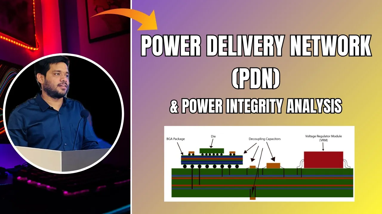

![10 preguntas de SMT [Tips consideraciones para diseño, fab y ensamble] Ft Editronikx](https://i.ytimg.com/vi_webp/98X9_dFBekg/maxresdefault.webp)
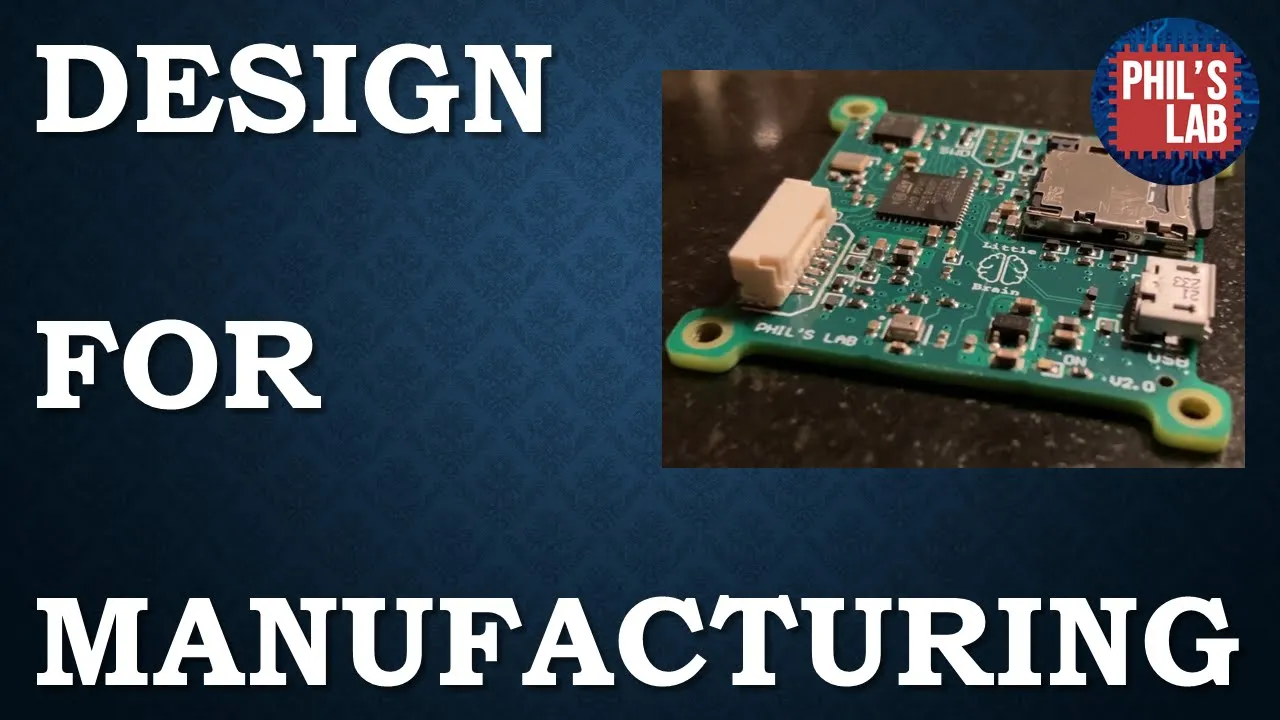
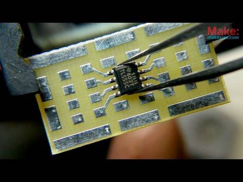
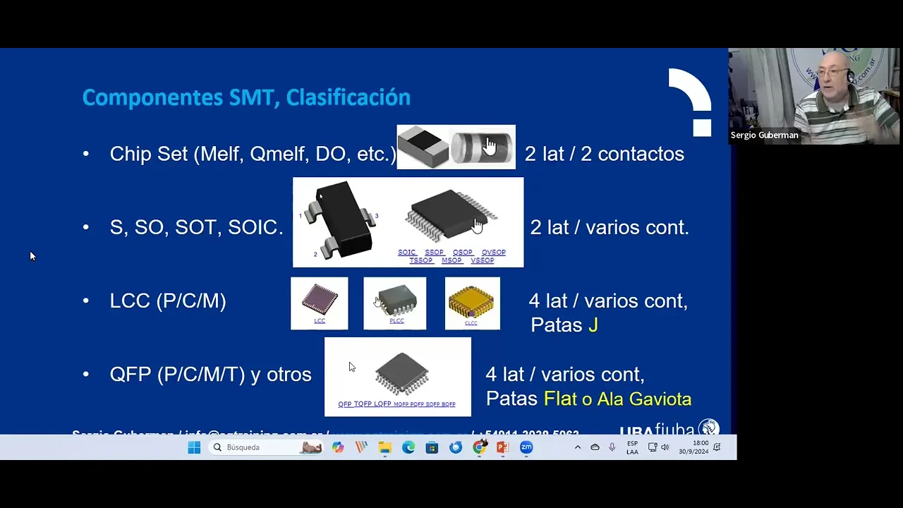







![끝판왕 보조배터리 자강두천 [앤커 VS 쿡테크]](https://i.ytimg.com/vi/_zcwJXNoyGc/maxresdefault.jpg)

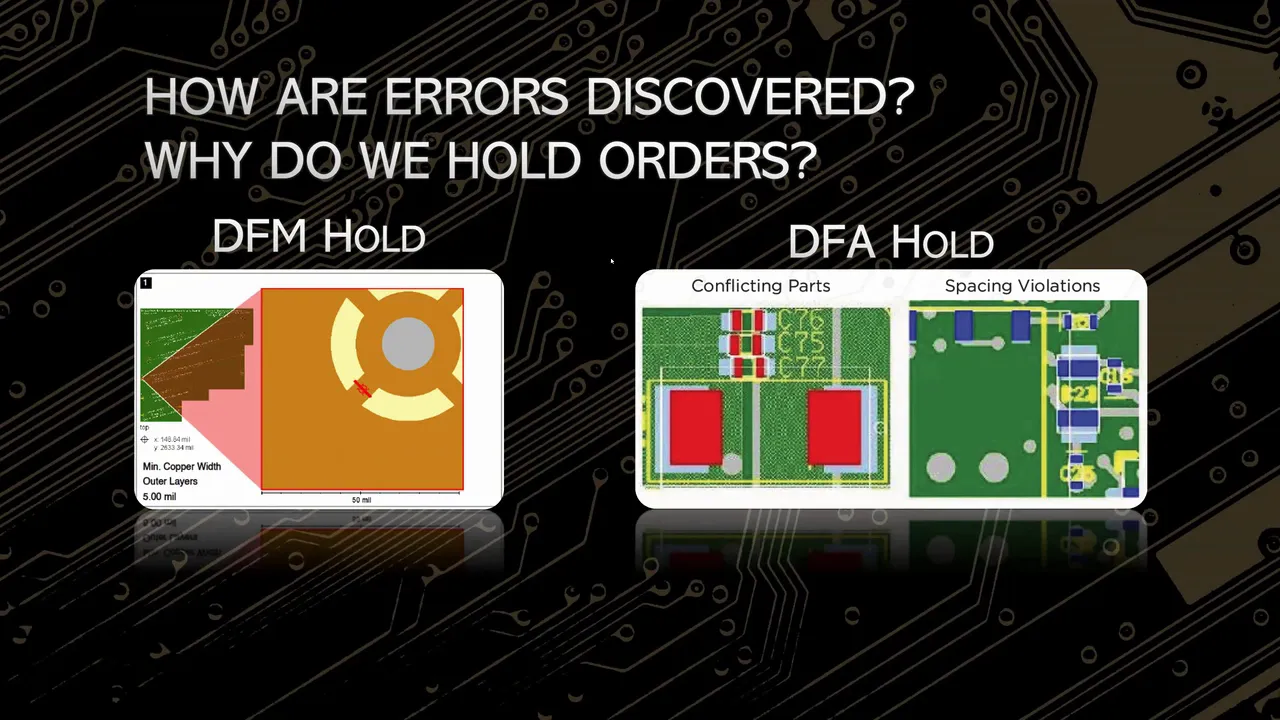


![Diseño para manufactura de PCB con normas IPC [DFM - Design for manufacturing ]](https://i.ytimg.com/vi/hZGGB1JQpFU/hqdefault.jpg)
A 4-layer PCB design allows for significantly more compact electronics by dedicating inner layers to ground (GND) and power (VCC) distribution, which frees up the front and bottom layers for signal routing and enables tighter component placement compared to traditional 2-layer PCBs.
4-Layer PCB Design: Transforming a GPS Emergency Device to Credit Card Size
Added:Fundamental understanding of schematic capture and basic 2-layer PCB layout design principles.
Basic concepts of Radio Frequency (RF) signals, including the importance of 50-ohm impedance matching for antennas.
An understanding of Power Distribution Networks (PDN) and how decoupling capacitors suppress noise in digital systems.
Familiarity with Surface Mount Technology (SMT) and small-scale component packaging (e.g., 0402, QFN, and BGA packages).
Advanced High-Speed Signal Integrity concepts, including controlled impedance routing, differential pairs, and via design.
Design for Electromagnetic Compatibility (EMC/EMI) to prepare wireless consumer electronics for FCC and CE certification testing.
Thermal management and heat dissipation strategies for ultra-compact, high-density electronic designs.
Design for Manufacturing (DFM) and Design for Assembly (DFA) methodologies for mass-producing multi-layer PCBs using High-Density Interconnect (HDI) technology.
416.3K views18.9Klikes10:18Original Release: 2022-01-23
This box can save your life is what I said during a previous project video because as soon as you press its big red button it either calls your phone to get you out of awkward conversations or if you select SMS mode it will send its GPS coordinates as an SMS to a contact of your liking in case you are in an emergency situation.
In my opinion it is a pretty useful box and that is also what lots of people said underneath the original project video which you should definitely check out.
The only problem I have with it is that it is a bit too big to carry around comfortably and or unnoticeable.
The reason is of course that the electronics system is made up of separate breakout boards that need to get connected to one another and that obviously takes up space.
So what I did to solve this problem was creating this almost credit card sized PCB onto which all components should snugly fit and hopefully still work well together.
So in this video we will not only find out whether this PCB does its job just fine but I will also tell you a bit more about how I designed it because this PCB is a 4 layer PCB and thus a bit more special than the 2 layer PCBs I usually use.
Let's get started This video is sponsored by JLCPCB which is the PCB manufacturer that produced the 4 layer PCBs for this project.
But they do not just make excellent quality PCBs nowadays, they also offer a 3D printing service in case you do not have a 3D printer at home and they also offer an SMD assembly service in case you are not into hand soldering or want to speed up your PCB assembling process.
So feel free to have a look at their website and be amazed what they can all do for very little money.
When starting this project I initially thought that it will be easy finding the main chips of the GSM and GPS board online but probably due to the semiconductor shortage that was not possible at all.
And that is why I was very thankful to have some spare boards lying around.
So the basic idea is removing the main chips of those boards, placing them onto a custom PCB with all the required complementary components they need and then adding an Arduino Pro mini as the microcontroller and a TP4056 IC as the charge circuit for the LiPo battery.
And at first that sounded simple enough but as soon as I realized that the used A6 GSM module and Neo-6M GPS module both came with datasheets that didn't feature a typical application schematic, I knew it wouldn't be super easy.
But luckily there are sites around with more details and eventually I even found a schematic around the GSM module as well as around the GPS module.
So I was time to find both of those modules in EasyEDA, place them in the schematic and make the necessary connections to their required complementary components and voltages.
And after I decided on a suitable uFL connector for the antennas, an EEPROM for the GPS board, a SIM card holder and an ESD protection IC which sits between the GSM module and SIM card holder and basically prevents electrostatic discharges, I finished the schematic around those modules and moved on to the TP4056 LiPo charging IC.
Its datasheet actually comes with a very simple example circuit and since I worked with it before it was no problem implementing it.
And last but not least I added an Arduino Pro Mini board around which I positioned and wired up pretty much the same components as shown in the previous iteration of this project except that this time they were mostly SMD versions of the components.
And just like that I had some faith that this schematic could work but more about the schematics problems later.
Because now it was time to convert this schematic to a PCB and for that I started off by simply placing the outlines of the components onto the front and bottom layer how I thought it would make sense.
Here is the final result with the Arduino, GPS and interface stuff on the top and the GSM and LiPo charging components on the back.
And that was the moment I clicked on my layer manager and switched from 2 copper layers to 4 and the reason for that is quite obvious because with 4 layers you simple have more copper layers for routing your signal and voltage lines and thus you can squeeze your components tighter together.
Of course there are more professional reasons like EMC problems but let's keep it simple for now and as an example have a look at this 2 layer design I created before.
As you can see on the real life board and in the design I used traces to connect the signal and voltage lanes of the components pins to one another on the top and bottom side.
By the way to connect the top with the bottom you utilize so called vias which look like this on the board.
But anyway at the end I then always use the copper area tool to create one big solid copper area on the top and bottom that features a small clearance to all the other traces while connecting all the GND pins of the components.
This method of course works just fine but by going 4 layers we can set one inner layer as the GND layer and the other one as the VCC or supply voltage layer.
This way we can simply set a via next to a voltage pin to jump to one of the inner layers and are therefore left with the complete front and bottom side for all the other signals which gives you so much more space and freedom to design.
I highly recommend trying that out but for my design I quickly realized that I didn't have time on my hand to route all the copper traces by myself.
So I did the unthinkable and used the autorouter which is a crime to some but I think while it did made some questionable choices regarding the power wiring, I was OK with the rest and thus quickly ordered the boards from JLCPCB for a great price along with of course a stencil for both sides.
And as soon as the PCBs and stencil arrived along with all the other components, it was finally time to use some hot air in order to free the GPS and GSM modules from their PCBs.
Afterwards I used the stencil in order to evenly spread the solder paste onto the first side of the PCB and that worked out pretty great.
So I placed all the components on this side and once again use hot air to melt the solder and thus basically secured all the components in place.
After then using some isopropanol for cleaning, I moved on to the other side which honestly speaking was pretty much the same thing as before and thus not very hard to do.
And after double checking that there were no shorts between the SMD pins and all solder connections looked good, it was time to move on to the through hole components which were a walk in the part in comparison to the SMD stuff.
And just like that the assembly was complete and I continued by adding test wires and powering the PCB with my lab bench power supply which to my delight didn't let anything explode.
But the current consumption seemed a bit low and thus I was a bit scared to check whether the GPS and GSM module were working properly.
And as you can see the GPS module did work while the GSM module was sadly not responding to my commands.
So it was time for troubleshooting which I did by checking the voltages on the original breakout board and then comparing that to my PCB version while also reverse engineering the original breakout board circuit.
And guess what; these two resistors were the problem that tie the power key pin and interrupt pin to the supply voltage which I thought is required according to the datasheet.
But apparently connecting the power pin to GND through a 10kohm resistor is the way to go.
And just like that the GSM status indicator LED came to life and it seems like all problems were solved.
So I hooked up a LiPo battery to test whether charging works which it did and then hooked up the antennas and inserted the SIM card before finally programming the microcontroller.
And as you can see the call mode works without a problem and after positioning the system outside we can see the GPS indicator LED blinking and thus sending the GPS location was also no problem.
Of course as a final touch I also designed a new enclosure for the project which I then 3D printed and through the help of the M3 holes in the corners of the PCB it was all very easy to put together.
And there you have it; a really useful project that is now a lot smaller and thus easier to carry around.
With that being said I hope you enjoyed this video and maybe learned a thing or two along the way.
If so consider supporting me through Patreon.
As always don't forget to like, share, subscribe and hit the notification bell.
Stay creative and I will see you next time.
Up Next

9:39
Keplerian Orbital Elements: Size, Shape, and Orientation
@alfonsogonzalez-astrodynam2207
16.8K views•2021-12-30

30:32
Ultrasonic Transducers: Resonant Frequency Measurement and Horn Design
@imajeenyus42
229.9K views•2017-02-22
5:54
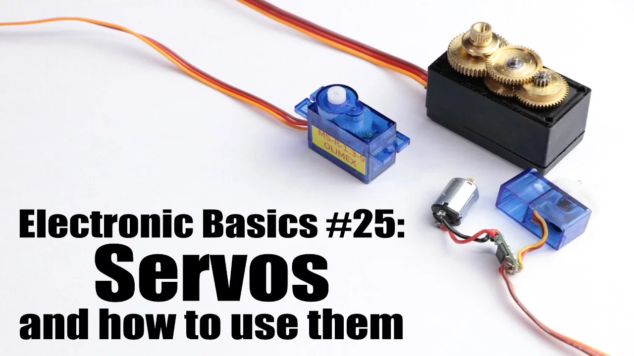
Understanding Servo Motors: How They Work & How to Use Them
@greatscottlab
977K views•2016-10-23
33:39
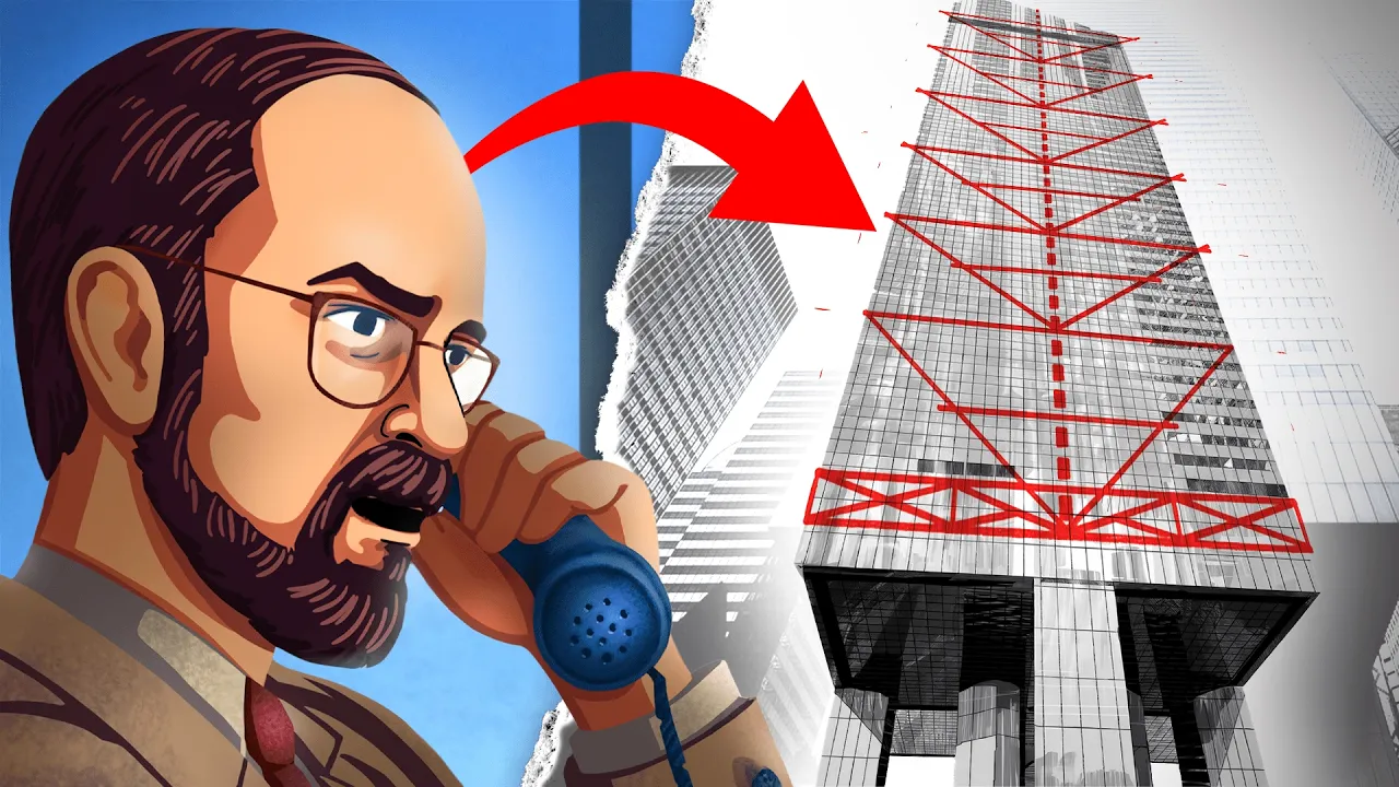
How a Student's Question Saved a NYC Skyscraper from Collapse
@veritasium
22.8M views•2025-04-26
Related Study Plans & Knowledge Roadmaps
Structured learning paths in Engineering
engineering
Building Acoustic Levitators: Physics & Arduino
01The Physics of Sound and Standing Waves
02Piezoelectric Transducers and H-Bridge Drivers
03Arduino Programming: Generating 40 kHz Signals
+ 2 more learning modules
14h5 modules
Explore Roadmap
engineering
Building Peltier Cloud Chambers: Particle Tracks
01Cosmic Rays & Cloud Chamber Physics
02Thermoelectric Cooling (TEC) Fundamentals
03Custom Liquid-Cooling Loop Design
+ 2 more learning modules
18h5 modules
Explore Roadmap
engineering
Yagi-Uda Antennas: Modeling, Build & VNA Test
01Introduction to RF and Antenna Fundamentals
02Yagi-Uda Antenna Design Principles
03Antenna Modeling and Simulation in 4NEC2
+ 2 more learning modules
18h5 modules
Explore Roadmap
engineering
ECG Monitor Design: Op-Amps, Filters & Noise
01Electronics & Breadboard Basics
02Op-Amps and Instrumentation Amplifiers
03Bioelectricity and ECG Fundamentals
+ 2 more learning modules
18h5 modules
Explore Roadmap