This video demonstrates how to design and simulate a Twin T Notch Filter (band-stop filter) using LTSpice software, showing the process of setting component values (resistors and capacitors), configuring AC analysis parameters, and verifying the filter's frequency response to achieve the desired stop frequency of approximately 1,346 Hz.
Designing a Twin T Notch Filter in LTspice: Band Stop Tutorial
Added:Deep Dive
Basic AC circuit theory, including the concept of capacitive reactance and impedance.

AC Theory Important Questions 🔥 | Electrician Theory for All Exams | ALP, Technical Helper 2025
10.2K
This section covers AC circuit reactance and impedance: (1) Inductive reactance X_L = 2πfL is zero in DC circuits (f=0), (2) X_L is directly proportional to frequency and inductance, (3) Capacitive reactance X_C = 1/(2πfC) is inversely proportional to frequency and capacitance, (4) Calculation example: 40mH coil at 1000Hz gives X_L = 251.2Ω, (5) Susceptance (B) is reciprocal of reactance, unit is Siemens (S), (6) Impedance (Z) unit is Ohm (Ω), (7) In purely resistive AC circuit, Z = R, (8) For circuit with X_L = 6Ω and X_C = 8Ω, Z = √(R² + (X_L - X_C)²) = 2Ω, (9) For R = 15Ω and Z = 25Ω, reactance X = √(Z² - R²) = 20Ω. These concepts are essential for understanding AC circuit behavior.
Click to watch →
Explained! Impedance, Admittance, Reactance, Inductance, Capacitance, Conductance, and Susceptance
121.8K
Impedance (Z) is a complex number representing total opposition to AC current flow, expressed as Z = R + jX in ohms. Resistance (R) is the real component opposing current without phase shift, while reactance (X) is the imaginary component opposing changes in current or voltage. Reactance has two types: inductive reactance (X_L = ωL = 2πfL) opposes current changes through magnetic field buildup, and capacitive reactance (X_C = 1/(ωC) = 1/(2πfC)) opposes voltage changes through charge storage between plates. Inductive reactance consumes reactive power (positive VARs) causing lagging power factor, while capacitive reactance supplies reactive power (negative VARs) causing leading power factor. Capacitors improve power factor by reducing the reactive power gap between apparent power (S) and real power (P).
Click to watch →

FIR315 S15 C1 JDDVP
137
This segment covers capacitive reactance (X_C) and impedance (Z) in AC circuits. The instructor explains that capacitive reactance is given by X_C = 1/(ωC) = 1/(2πfC), where ω is angular frequency, f is frequency, and C is capacitance. Unlike inductive reactance, capacitive reactance decreases as frequency increases. The instructor then introduces impedance as the total opposition to current flow, combining resistance, inductive reactance, and capacitive reactance. For series RLC circuits, impedance is calculated as Z = √(R² + (X_L - X_C)²).
Click to watch →
What is Resistance, Inductance, Capacitance and Impedance|| R, L, C & Z क्या है???
53K
A capacitor consists of two conducting plates separated by an insulating dielectric material. When connected to a voltage source, charge accumulates on the plates, storing electrical energy in the electric field between them. Capacitance is the ability to store charge, measured in Farads (F). Capacitive reactance is the opposition a capacitor offers to AC current, which is inversely proportional to both frequency and capacitance. In AC circuits, total opposition to current flow is called impedance (Z), which combines resistance, inductive reactance, and capacitive reactance into a single complex quantity measured in Ohms.
Click to watch →
![[긴급학습지원] 대학생 전기 1. 회로이론_제3장 RLC 교류회로](https://i.ytimg.com/vi_webp/i7ckFBfh8Is/maxresdefault.webp)
[긴급학습지원] 대학생 전기 1. 회로이론_제3장 RLC 교류회로
4K
This section covers capacitive reactance and the concept of impedance in AC circuits. Capacitive reactance is calculated using XC = 1/(ωC), where ω is angular frequency and C is capacitance. The voltage across a capacitor is given by V = -j/(ωC) × I, where the negative sign indicates that voltage lags current by 90 degrees. In capacitive circuits, current leads voltage by 90 degrees, which is the opposite of inductive circuits. The section then introduces impedance (임피던스, Z) as the total opposition to current flow in AC circuits, combining resistance (R) and reactance (X), measured in ohms. For RL circuits, Z = R + jωL. For RC circuits, Z = R - j/(ωC). For RLC circuits, Z = R + j(ωL - 1/(ωC)). The magnitude of impedance is |Z| = √(R² + X²). The instructor emphasizes that impedance is a complex quantity that accounts for both magnitude and phase relationships, making it essential for AC circuit analysis.
Click to watch →
Deep Dive
Fundamentals of filter characteristics, specifically the definition and behavior of a band-stop (notch) filter.
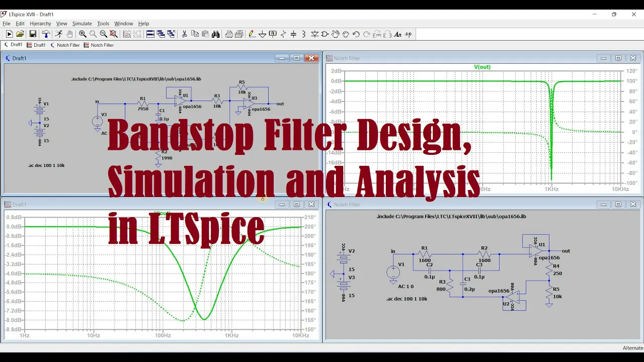
Band Stop Filter | Band Reject Filter Explained | Analysis | Simulation #notch #ltspice #diy
6.6K
A band stop filter is created by combining an RC low pass filter with an RC high pass filter, functioning to block or severely attenuate frequencies within a specific range while passing all others. Also called a band reject or notch filter, it operates as the inverse of a band pass filter. The filter is second-order with two cutoff frequencies (-3 dB points) defining a wide stop band. It passes frequencies below the lower cutoff (f_low) and above the upper cutoff (f_high), while rejecting frequencies in between. When the stop band is extremely narrow and highly attenuated, it becomes a noise filter. The geometric mean of the cutoff frequencies determines the center frequency, and the Q factor represents the ratio of center frequency to bandwidth.
Click to watch →

Band Reject Filter ( BRF ) / Band Stop Filter (BSF) | Band Stop/Reject Filter | Analog BPF/BRF
361
A band reject filter (band stop filter or notch filter) is an electronic circuit that blocks signals within a specific frequency range while allowing signals outside that range to pass through. The ideal transfer function magnitude |H(jω)| shows pass bands at frequencies below ωC1 and above ωC2 with |H(jω)| = 1, and a stop band between ωC1 and ωC2 with |H(jω)| = 0. Practical applications include removing power supply interference (50 Hz or 60 Hz hum) from electronic devices and audio systems. A notch filter is a highly tuned version of a band reject filter designed to eliminate a single specific frequency.
Click to watch →

L28 | Designing of BSF using LPF and HPF, Designing of APF, Problems Based on Filters (Part-01)
6.6K
Band-stop filters exhibit a frequency response with a notch at the center frequency where the gain drops to zero. The filter allows low frequencies to pass through and high frequencies to pass through, while blocking a specific middle frequency band. The frequency response is discontinuous, which is why bandwidth is not defined for band-stop filters. The notch filter is a special case where rejection occurs at a single specific frequency rather than a band.
Click to watch →

L02 Complete OP-AMP Revision | GATE 2026 | Best Practise Session #gateacademy
2.2K
This section provides a comprehensive overview of filter classification and band-stop filter design principles. Filters are classified based on their frequency response characteristics: Low-pass filters pass low frequencies and attenuate high frequencies. High-pass filters pass high frequencies and attenuate low frequencies. Band-pass filters pass a specific frequency band while attenuating frequencies outside this band. Band-stop (notch) filters attenuate a specific frequency band while passing frequencies outside this band. All-pass filters pass all frequencies with unity magnitude but introduce phase shift. For a band-stop filter, both low and high frequencies are passed while a specific band is attenuated. The transfer function for a second-order band-stop filter is T(s) = (s² + ω₀²)/(s² + (ω₀/Q)s + ω₀²). At both DC (s = 0) and infinite frequency (s → ∞), the gain is 1. At the center frequency ω₀, the gain is zero. Band-stop filters are also called notch filters or band-reject filters. The bandwidth is not defined in the same way as for band-pass filters since both low and high frequencies are passed. The quality factor Q determines the sharpness of the notch. A higher Q value results in a narrower notch. An all-pass filter can be designed using a low-pass filter topology. The transfer function is T(s) = (1 - sRC)/(1 + sRC). This form has a zero at s = 1/(RC) and a pole at s = -1/(RC). The phase response is φ(ω) = -2tan⁻¹(ωRC). At ω = 0, φ = 0°. At ω → ∞, φ = -180°. This design uses the low-pass filter topology but produces the same all-pass behavior as the high-pass design. The pole-zero diagram shows a zero at s = 1/(RC) and a pole at s = -1/(RC). The distance between the zero and the origin equals the distance between the pole and the origin, which is a characteristic property of all-pass filters. This configuration makes all-pass filters non-minimum phase systems.
Click to watch →

Band-stop Filter Design with two operational amplifiers
852
In the s-plane, the notch filter exhibits specific pole-zero placement: zeros lie on the imaginary axis at ±jω₀, while poles are located near the imaginary axis with small negative real parts. At DC (s=0), the numerator and denominator vectors are approximately equal in magnitude, resulting in gain of 1. At high frequencies (s→∞), the highest-order terms dominate and again yield gain of 1. Exactly at the zero frequency (ω=ω₀), the numerator becomes zero regardless of input, producing zero output - confirming the notch behavior.
Click to watch →
Deep Dive
Introductory proficiency in LTspice, including placing components, wiring, and running basic schematic drafts.

001 LTspice introduction, component placement, wiring and simulation
653
LTspice is a powerful circuit simulation tool for electronics and electrical engineers. Download from analog.com via Design Resources > Design Tools and Calculators. The interface includes: new schematic button, run button (green arrow), zoom tools, cut/copy/paste, wire tool (pencil), ground symbol, net labeling, component library, move/drag, undo/redo, mirror imaging, text tool for comments, and SPICE directive tool. Keyboard shortcuts: R=resistor, C=capacitor, D=diode, L=inductor, V=voltage source, G/Z=ground, I=current source. Place components using shortcuts or library. Wire components using the wire tool. Set component values by right-clicking (e.g., 10K for resistors, 15V for voltage sources). Run simulation by specifying stop time and start time. View results using the probe tool (pen symbol) to measure node voltages. The error log identifies missing values, helping diagnose issues early.
Click to watch →

Experiment #3x: Simulation of Circuits Using LTspice (including) LTspice tutorial
1.9K
LTspice is a circuit simulator accessible via personal installation or UIC Virtual Lab remote desktop. For Virtual Lab, type 'desktop uic edu', sign in with UIC credentials, then log into remote desktop. Windows and Mac interfaces differ: Windows uses top menu bar, Mac requires right-clicking the program. To start a new schematic, click the 'New Schematic' icon. Basic components needed are voltage sources, current sources, resistors (2-5), and ground symbol. To place components, click the Component icon, select the component (e.g., Voltage), and click OK. Components snap to grid positions. Multiple copies are created by clicking and dragging. Exit placement mode by pressing Escape or right-clicking. LTspice automatically numbers components with reference designators (V1, V2 for voltage sources, R1, R2 for resistors). To rename, right-click and type the new name. To set values, right-click on the value field and enter the desired value.
Click to watch →

Intro to LTSpice
248.6K
This section covers the essential steps for beginning circuit simulation in LTSpice. Users learn to download and install the software, create new schematics, and display the grid for accurate component placement. The tutorial demonstrates adding fundamental components including voltage sources, resistors, operational amplifiers, and ground connections. Key concepts include understanding spice directives like 'liopamp.sub' for ideal op-amps, using the wire tool for circuit connections, and rotating components using the rotate button or Ctrl+R. The section emphasizes that LTSpice wires don't bend automatically and must be manually adjusted.
Click to watch →

LTSpice Tutorial - EP1 Getting started
842.9K
To create a circuit schematic in LTspice, you need to place basic components including resistors, voltage sources, and ground references. Resistors can be placed by clicking the resistor icon in the toolbar or by pressing the R key. Voltage sources are found in the components menu at the end of the list. Ground symbols provide the reference point for all voltages in the circuit. Components can be connected using the wire tool, which automatically links components without causing short circuits.
Click to watch →

LTSpice Presentation with Andrea Urueta | TAMU SHPE
161
LTSpice provides a schematic drawing interface with control icons for zooming, copying, pasting, placing components, connecting with wires, adding grounds, labels, and moving/rotating components. Components are placed via the component button (NAND icon) or F2 key, with options to search for resistors, capacitors, inductors, diodes, and transistors. Components can be rotated with Ctrl+R and mirrored with Ctrl+E. Circuit connections use the wire tool (F3), and every circuit requires a ground symbol (G key). Component values use specific notation: K for kilo (10^3), M for mega (10^6), U for micro (10^-6). Critical: use 'Meg' not 'M' for mega values since 'M' is reserved for milli.
Click to watch →
Deep Dive
The operating principles of passive RC low-pass and high-pass filter networks, which form the building blocks of the Twin-T topology.

#380: Circuit Fun: Twin-Tee Oscillator - low distortion op amp sine waves
52.1K
The twin-T network consists of two T-style filters connected in parallel. One branch is an R-C-R low-pass filter that shunts high frequencies to ground, while the other branch is a C-R-C high-pass filter. When configured with specific relationships between component values (R values are equal, and capacitor values are doubled in one leg), these circuits resonate at the same frequency. This creates a notch filter response where the combined circuits produce a deep attenuation at the resonant frequency, typically around 40-50 dB deep, making it effective for removing unwanted frequencies like 60 Hz or 120 Hz interference.
Click to watch →

Passive RC low pass filter tutorial!
906.2K
A passive RC low-pass filter is a simple circuit consisting of a resistor and capacitor that allows low-frequency signals to pass through while attenuating high-frequency signals; the filter's cut-off frequency is determined by the formula f_c = 1/(2πRC), where at frequencies below the cut-off point the signal passes unchanged, and above this point the amplitude decreases at a rate of approximately 20 decibels per decade, with the cut-off frequency representing the point where the amplitude is reduced by approximately 30% (or 3 dB).
Click to watch →
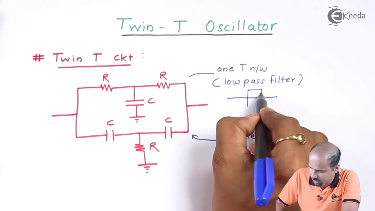
Twin -T Oscillators | Electronic Devices and Circuits 2 in EXTC Engineering
5.5K
The Twin-T Oscillator is a low-frequency oscillator circuit that combines two T-networks (one acting as a low-pass filter and the other as a high-pass filter) connected in parallel, where the low-pass filter has resistors in series with a shunt capacitor and the high-pass filter has capacitors in series with a shunt resistor; when both networks are configured with the same cutoff frequency, they form a band-reject filter that enables sustained sinusoidal oscillation at a specific frequency determined by the RC time constant, with the oscillation frequency given by f₀ = 1/(2πRC).
Click to watch →
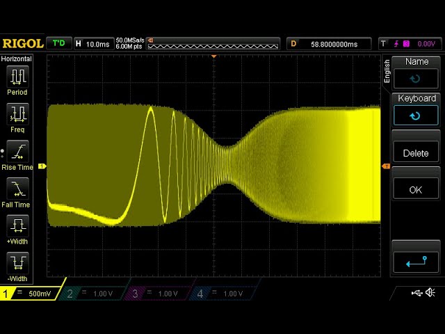
#471 Twin T Filter
2.4K
T-filters are fundamental passive filter circuits shaped like the letter T, consisting of three components arranged in specific patterns. The resistor-resistor-capacitor (RRC) configuration functions as a low-pass filter, allowing low frequencies to pass while attenuating high frequencies because capacitors block DC and low-frequency signals but allow high-frequency AC to bypass to ground. Conversely, the capacitor-capacitor-resistor (CCR) configuration acts as a high-pass filter, permitting high frequencies while blocking low frequencies. Both configurations use identical component values (10kΩ resistors and 0.01μF capacitors) and demonstrate complementary frequency response characteristics when tested with an oscilloscope using a logarithmic frequency sweep from 1 Hz to 1 MHz, with the cut-off frequency occurring around 1 kHz for these particular component values.
Click to watch →

Passive RC Filters
5.9K
Passive RC filters are fundamental circuit elements that use resistors and capacitors to create frequency-selective responses; they work by exploiting the frequency-dependent impedance of capacitors (which decreases with increasing frequency) combined with the constant impedance of resistors, enabling the construction of basic filter types including high-pass, low-pass, band-pass, and band-stop configurations, with more advanced designs like twin-T notch filters and limited-attenuation filters offering greater control over frequency response characteristics.
Click to watch →
Prerequisite Knowledge
- Concept 01Basic AC circuit theory, including the concept of capacitive reactance and impedance.
- Concept 02Fundamentals of filter characteristics, specifically the definition and behavior of a band-stop (notch) filter.
- Concept 03Introductory proficiency in LTspice, including placing components, wiring, and running basic schematic drafts.
- Concept 04The operating principles of passive RC low-pass and high-pass filter networks, which form the building blocks of the Twin-T topology.
Subsequent Learning
- Step 01Design of active Twin-T notch filters using operational amplifiers to improve selectivity and Q-factor.
- Step 02Performing Monte Carlo tolerance analysis in LTspice to evaluate how real-world component variations degrade the notch depth.
- Step 03Practical applications of notch filtering, such as eliminating 50Hz/60Hz power-line hum in audio systems or ECG sensor readings.
- Step 04Exploration of alternative notch filter topologies, such as the Bainter, Fliege, or Wien-Bridge configurations.
Filter Design
Param Testing
Filter Design
0:00Playing Section
- 1
Sets up a 20-notch filter circuit with equations and components.
- 2
Places voltage source, ground, resistors, and capacitors on the schematic.
Real-World Component Sensitivity and the Superiority of Active Filter Topologies
While LTspice simulations of a passive Twin-T notch filter show an ideal, deep attenuation at the target frequency, this theoretical performance rarely translates to physical circuits due to extreme sensitivity to component tolerances. In practice, even a 1% mismatch in resistor or capacitor values severely degrades the notch depth and shifts the center frequency. To achieve a reliable, high-Q stopband in real-world applications, engineers often reject the passive Twin-T design in favor of active filter topologies, such as the Bainter, Fliege, or State-Variable notch filters. These alternative designs offer much lower sensitivity to component variations, allow for independent tuning of the notch frequency and quality factor (Q), and provide buffered outputs, making them far more robust and practical than the highly temperamental passive Twin-T configuration.
Deep Dive
Design of active Twin-T notch filters using operational amplifiers to improve selectivity and Q-factor.
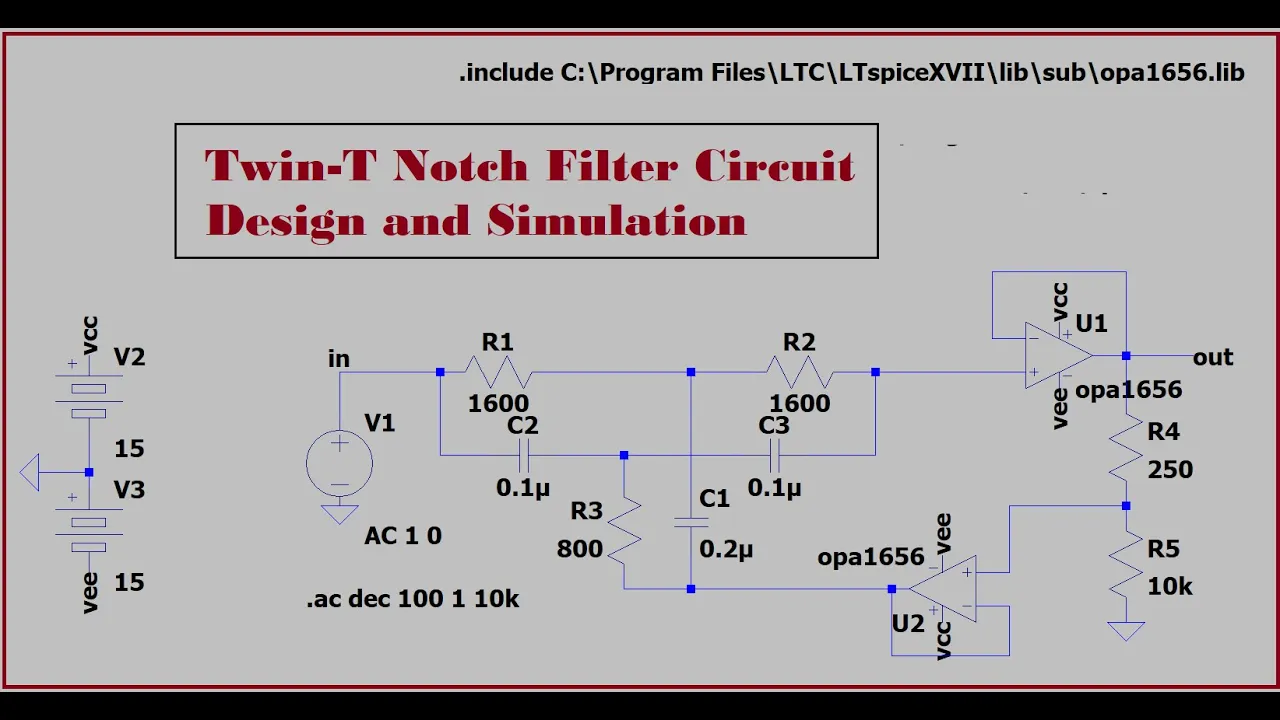
🔥🔥Twin-T Notch Filter Circuit Design, Simulation Analysis in LTSpice🔥🔥#circuit #ltspice #tutorial
4.9K
A Twin-T notch filter is a narrowband band-stop filter that blocks a specific frequency range while passing all others; it consists of two T-networks (one low-pass and one high-pass) connected in parallel, with the notch frequency calculated as f₀ = 1/(4πRC), where the low-pass section uses twice the capacitance and twice the resistance of the high-pass section. The Q factor determines selectivity, with higher Q values producing narrower notches and greater attenuation. Active implementations using operational amplifiers like the OPA1656 provide better performance than passive versions, achieving precise notch depth and bandwidth control through feedback networks.
Click to watch →

Twin-T Bandstop Filter Design 🌟 Transfer Function & Design Example! 🎯 #notch #filter
1.6K
The Twin-T bandstop filter is an active filter circuit that uses two T-networks with specific component ratios (resistors and capacitors in 2:1 relationships) along with operational amplifiers as voltage buffers. The transfer function shows a second-order system with a center frequency ω_center = 1/(RC) and bandwidth ω_bw = 4(1-x)/RC, where x = 1 - 1/(4Q) and Q is the quality factor (ratio of center frequency to bandwidth). For a narrow band notch filter design with center frequency of 400 Hz and bandwidth of 40 Hz (Q = 10), selecting C = 10 nF yields R = 40 kΩ, R1 ≈ 39 kΩ, and R2 ≈ 1 kΩ. Simulation verification using Bode plots confirms the design meets specifications with a sharp notch at the center frequency and correct passband gain.
Click to watch →

OP-AMP NARROW BAND REJECT FILTER OR NOTCH FILTER(Variable Q)
369
A variable Q notch filter (narrow band reject filter) uses two OP-AMPs in voltage follower configuration with a feedback network to achieve adjustable quality factor, unlike the basic 20-network notch filter which has a fixed Q of 0.25; the variable Q filter allows Q to be controlled by adjusting the feedback factor K=R2/(R1+R2), enabling precise single-frequency rejection with narrower bandwidth as K approaches unity.
Click to watch →

APRENDA A PROJETAR UM FILTRO REJEITA BANDA ATIVO (TEORIA E PRÁTICA)
10.5K
An active band-reject filter using the Dual-T topology with operational amplifiers can be designed by selecting component values that satisfy the cutoff frequency equation fc = 1/(2π × R1 × C1) and the quality factor equation Q = (Ra + Rb)/(4 × Ra), where R1 = R2 = 2 × R3 and C1 = C2 = ½ × C3; the filter attenuates signals at the cutoff frequency while allowing frequencies above and below to pass, with different Q values producing Bessel, Butterworth, or Chebyshev response approximations.
Click to watch →
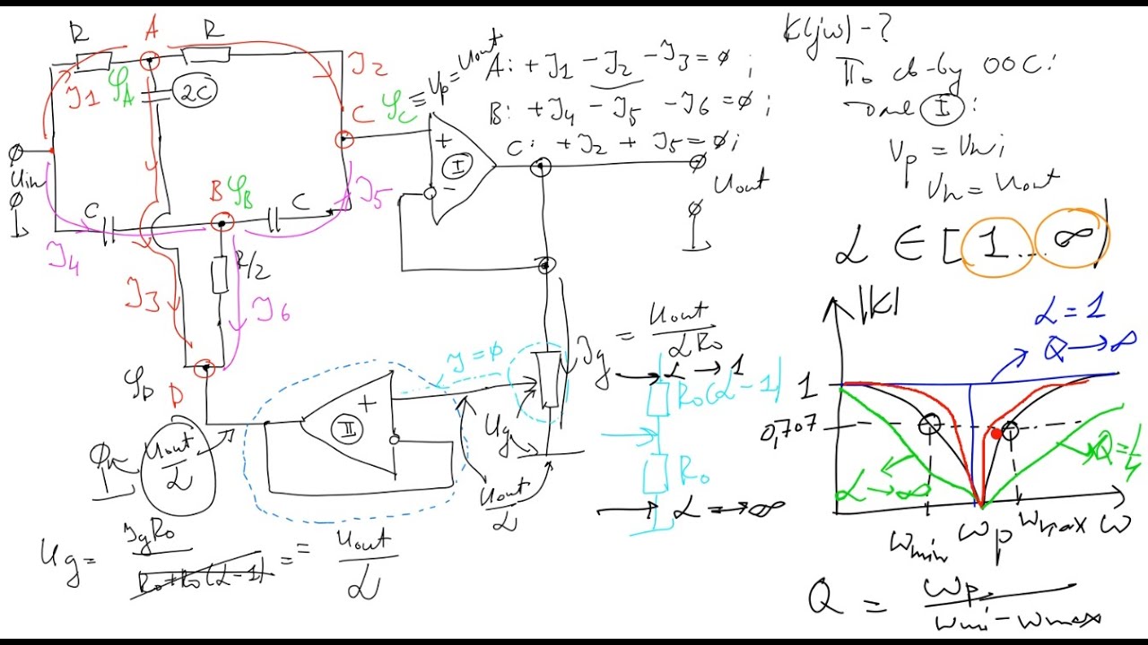
Активные фильтры на операционных усилителях (3 часть).
1.7K
The twin-T notch filter employs a double-T bridge configuration followed by an operational amplifier buffer. The bridge consists of two T-networks with a potentiometer controlling the balance between arms. The buffer provides high input impedance and low output impedance, isolating stages while preserving signal integrity. The mathematical analysis involves writing node equations for each junction, applying op-amp properties, and deriving the transfer function. The magnitude response shows complete rejection at the notch frequency, with the quality factor adjustable from 1/4 to infinity through the potentiometer setting.
Click to watch →
Deep Dive
Performing Monte Carlo tolerance analysis in LTspice to evaluate how real-world component variations degrade the notch depth.
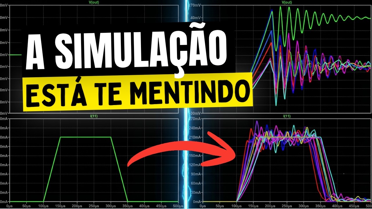
Como evitar que seu Protótipo FALHE: Simulação Realista no LTSpice
136
This video explains three methods for incorporating component tolerances into circuit simulations using LTspice: Worst Case Analysis (pessimistic, evaluates extreme conditions by varying all components to their tolerance limits), Monte Carlo with Uniform Distribution (randomly selects values across the entire tolerance range, useful when manufacturer data is unavailable), and Monte Carlo with Gaussian Distribution (most realistic, models actual manufacturing variations where most components cluster near nominal values with 68.2% within one standard deviation). The Gaussian distribution requires dividing the tolerance by 3 since LTspice interprets the input as standard deviation. These methods help minimize hardware prototype failures by accounting for real-world component variations.
Click to watch →
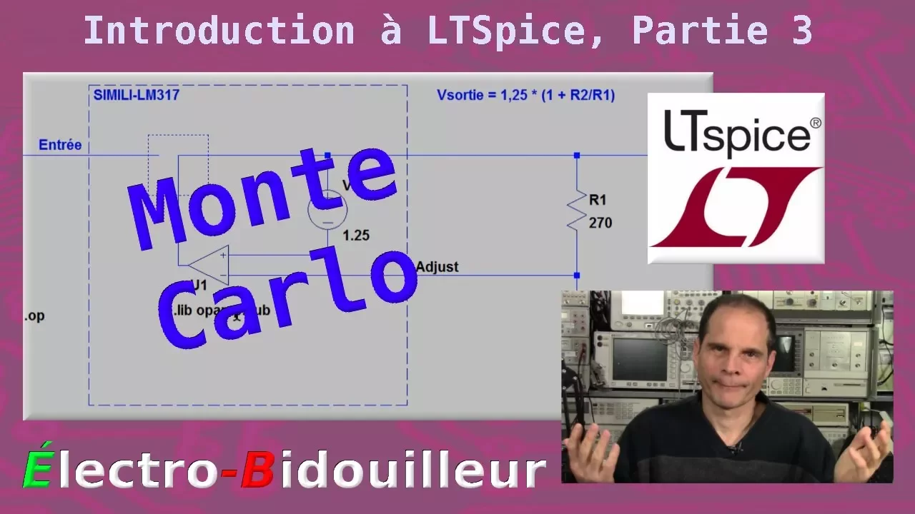
EB_#195 Introduction à LTSpice, Partie 3: Simulation Monte Carlo
14.8K
Monte Carlo simulation in LTSpice is a statistical analysis technique that calculates circuit response by randomly varying component parameters within specified tolerance limits across multiple iterations, allowing engineers to predict and analyze how real-world component variations affect circuit performance and identify worst-case scenarios.
Click to watch →

Monte Carlo Simulation in LTspice | LTspice tutorial #ltspice #montecarlo
4.1K
Monte Carlo analysis in LTspice is a statistical simulation technique that evaluates how component tolerances affect circuit performance by randomly varying component values within specified tolerance ranges (e.g., ±10%) and running multiple simulation iterations to determine the statistical distribution of output parameters, enabling circuit designers to predict and account for real-world manufacturing variations in their designs.
Click to watch →

LTSpice - Monte Carlo and Worst Case Simulations
20.8K
LTSpice provides Monte Carlo and worst case simulation tools to analyze circuit performance under component tolerance variations; Monte Carlo uses normal distribution to model realistic probability distributions of component values, while worst case analysis assumes all tolerances stack in the most unfavorable direction to identify absolute maximum/minimum performance scenarios, enabling designers to verify that their circuits will meet specifications across all possible component variations.
Click to watch →
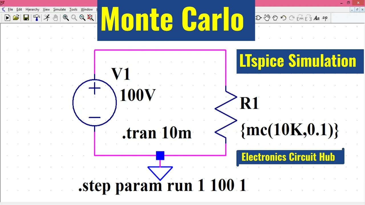
LTSpice Monte Carlo Circuit Analysis | Simulation
3.7K
Monte Carlo analysis is a statistical simulation method used to analyze circuit behavior and component tolerance by randomly varying component values within their specified tolerance ranges across multiple simulation iterations. In LTspice, this is implemented using the MC syntax (e.g., MC bres 10K, 0.1 for a 10K resistor with 1% tolerance) combined with a parameter sweep that runs multiple iterations (e.g., 100 times with step of 1). The simulation reveals how component tolerances affect circuit performance—for example, a 10K resistor with 1% tolerance in a 100V circuit will produce current values ranging from approximately 9mA to 11.17mA instead of the theoretical 10mA, demonstrating the real-world impact of manufacturing variations on circuit behavior.
Click to watch →
Deep Dive
Practical applications of notch filtering, such as eliminating 50Hz/60Hz power-line hum in audio systems or ECG sensor readings.
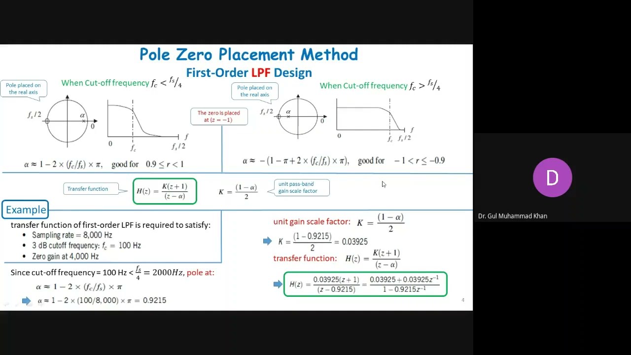
#Filters:Pole Zero Method First Order, #LPF Design, First Order Application #HPF Design,& applicatio
1.8K
This concluding section demonstrates practical applications of notch filter design in real-world scenarios. The instructor explains how power supply hum (50/60 Hz) contaminates electronic signals, particularly affecting sensitive measurements like ECG readings. Since power waveforms contain multiple harmonics (100 Hz, 150 Hz, etc.), single-notch filters prove insufficient. Students learn that cascading multiple notch filters, each targeting specific harmonic frequencies, provides effective multi-frequency suppression. The instructor connects this technical concept to medical applications, explaining how ECG signals containing P, Q, R, S, T waves require clean acquisition for accurate cardiac disease diagnosis. The section emphasizes that proper hum elimination preserves waveform integrity necessary for detecting the 16+ classes of heart conditions that rely on precise peak analysis.
Click to watch →
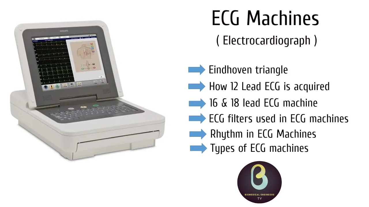
ECG Machines | Electrocardiograph | Biomedical Engineers TV |
27.2K
A notch filter or main AC filter combines both high-pass and low-pass characteristics to create a narrow band of frequencies to be removed. In ECG machines, the primary target is removing 50 Hz or 60 Hz mains noise, which falls within the diagnostic frequency region of interest. AC filter settings are usually optional since ECG equipment already contains some ability to reject mains noise through other mechanisms like the right leg drive. Some systems automatically detect mains frequency, while others are set by users or service personnel, with some covering both 50 and 60 Hz simultaneously.
Click to watch →

Every Type of Electronic Filter Explained
128
The notch filter is a different instrument entirely. Narrow Q, sharp edges, deep rejection at one specific frequency while everything immediately adjacent survives almost untouched. The most famous application is mains hum removal. Electrical power is delivered at 50 hertz in most of Europe, Asia, and Africa, and at 60 hertz in North America and parts of South America.
Click to watch →
What Do Microwaves Hum?
431.5K
A band-stop filter, also known as a notch filter, reduces specific frequency ranges while allowing most other frequencies to pass through. For mains hum reduction, filters are designed to completely reduce frequencies in the range of 49-51 Hz or 59-61 Hz. This range is chosen because actual power line frequencies fluctuate slightly (by a few thousandths of a Hz) based on supply and demand variations, rather than remaining perfectly at exactly 50 or 60 Hz.
Click to watch →
Lab: Filtering
1.2K
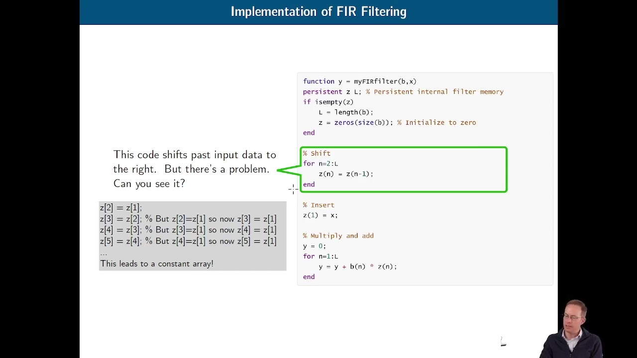
Practical filter applications demonstrate real-world signal processing tasks. Shelving filters boost or cut specific frequency ranges (e.g., +10 dB at low frequencies) while passing others unchanged, useful for audio equalization. Notch filters remove narrow frequency bands (e.g., eliminating 60 Hz hum or specific musical notes) through carefully designed coefficient relationships. Implementation requires converting recursive difference equations to standard form by adjusting feedback coefficient signs. Validation techniques include impulse response testing (applying impulse input should reproduce coefficients) and spectrogram analysis comparing input/output frequency content. These methods confirm filter correctness and enable practical audio processing applications.
Click to watch →
Deep Dive
Exploration of alternative notch filter topologies, such as the Bainter, Fliege, or Wien-Bridge configurations.
Wien Bridge Oscillator (using op-amp) Explained
538.2K
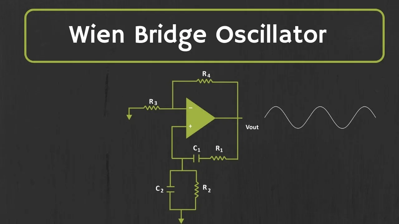
The RC feedback network in the Wien bridge oscillator functions as a notch filter. At the resonant frequency, the output of the circuit reaches its maximum value, while at all other frequencies, the output is minimized. At this specific resonant frequency, the phase shift of the circuit equals zero degrees, and the ratio of output to input (feedback fraction β) equals 1/3.
Click to watch →

Радиоэлектроника. Часть 6. Фильтры Вина-Робинсона, двойной Т-образный, 3-звенная RC для генератора.
306
This section covers notch (rejector) filter characteristics and practical applications. Notch filters do the opposite of bandpass filters: they attenuate a specific frequency while passing all other frequencies. The Wien bridge filter can be configured as a notch filter, rejecting a narrow frequency band. The lecture explains that notch filters are particularly useful for eliminating power line interference (50/60 Hz) from electronic circuits, as well as interference from nearby radio stations and parasitic signals in technical devices. The filter can be tuned to reject specific frequencies by adjusting component values.
Click to watch →

All about 2-pole RLC passive filters (7 - Passive Filters)
8.5K
Filter topologies are classified as series-fed (first reactive element in series) or shunt-fed (first reactive element shunted to ground). Series-fed topologies include inductor-first (low-pass), capacitor-first (high-pass), and series LC combinations (band-pass). Shunt-fed topologies use capacitors or inductors shunted to ground for low-pass or high-pass filtering respectively. Band-pass filters can also be shunt-fed with both elements to ground. A notch filter blocks a specific frequency range by having two zeros on the imaginary axis and two poles, with high-frequency signals passing through the capacitor and low-frequency signals through the inductor. Band-pass filters are essential in AM radio receivers, where tunable inductors or capacitors allow adjustment of the center frequency ω₀ = √(1/LC) to select different radio stations.
Click to watch →
Активные фильтры на операционных усилителях (3 часть).
1.7K
The twin-T notch filter employs a double-T bridge configuration followed by an operational amplifier buffer. The bridge consists of two T-networks with a potentiometer controlling the balance between arms. The buffer provides high input impedance and low output impedance, isolating stages while preserving signal integrity. The mathematical analysis involves writing node equations for each junction, applying op-amp properties, and deriving the transfer function. The magnitude response shows complete rejection at the notch frequency, with the quality factor adjustable from 1/4 to infinity through the potentiometer setting.
Click to watch →
A Better Way to Think About a Notch Filter | Control Systems in Practice
80.8K
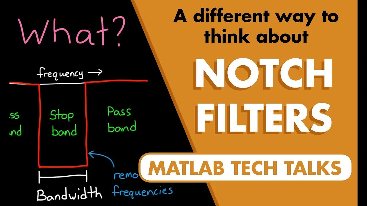
A notch filter can be intuitively understood as an inverted, lightly damped second-order low-pass filter (which creates a peak at the natural frequency) with two additional poles added to make it realizable and provide control over the notch width; the damping ratio controls the depth of the notch, the natural frequency determines its location, and the ratio of pole positions relative to the natural frequency controls the notch width.
Click to watch →
Filter Design
Param Testing
Filter Design
0:00- 1
Sets up a 20-notch filter circuit with equations and components.
- 2
Places voltage source, ground, resistors, and capacitors on the schematic.
Real-World Component Sensitivity and the Superiority of Active Filter Topologies
While LTspice simulations of a passive Twin-T notch filter show an ideal, deep attenuation at the target frequency, this theoretical performance rarely translates to physical circuits due to extreme sensitivity to component tolerances. In practice, even a 1% mismatch in resistor or capacitor values severely degrades the notch depth and shifts the center frequency. To achieve a reliable, high-Q stopband in real-world applications, engineers often reject the passive Twin-T design in favor of active filter topologies, such as the Bainter, Fliege, or State-Variable notch filters. These alternative designs offer much lower sensitivity to component variations, allow for independent tuning of the notch frequency and quality factor (Q), and provide buffered outputs, making them far more robust and practical than the highly temperamental passive Twin-T configuration.
Basic AC circuit theory, including the concept of capacitive reactance and impedance.
Fundamentals of filter characteristics, specifically the definition and behavior of a band-stop (notch) filter.
Introductory proficiency in LTspice, including placing components, wiring, and running basic schematic drafts.
The operating principles of passive RC low-pass and high-pass filter networks, which form the building blocks of the Twin-T topology.
Design of active Twin-T notch filters using operational amplifiers to improve selectivity and Q-factor.
Performing Monte Carlo tolerance analysis in LTspice to evaluate how real-world component variations degrade the notch depth.
Practical applications of notch filtering, such as eliminating 50Hz/60Hz power-line hum in audio systems or ECG sensor readings.
Exploration of alternative notch filter topologies, such as the Bainter, Fliege, or Wien-Bridge configurations.
435 views6likes4:09@dudekpobOriginal Release: 2025-02-10
hello welcome to my electronic basic course today I want to show you how to design basic 20 Notch filter it's a Bop filter you can see on the left side of the screen we have equation our P stop frequency equals like 1,3 46 HZ so let's do do this filter I Vol The Source ground F resistors and two capacitors three Capac sorry I mistake here here and okay now we need to go in this I present and click on this element okay now Escape come back to one okay [Music] think this network F out okay everything is ready now we need to like okay parameters par directive param l = 10 uh press shift and and enter par Capal 6 microfarads so okay now to cck this go to advance subed one go to l toose okay let's copy this multiply by two t two okay now we have see see okay so it's ready now can this you go to AC analysis table sweep choose the choose 20 1 2 to 100 okay so we have our plot take this you can see this is our parameter of our filter I 10 10,000 so this 100 so it's better you can see we have like go to place C see this is that frequency it's like one KZ one put 300 one 1,300 KZ so it's almost this is our our band
Up Next
35:07
How to Use an Oscilloscope: A Beginner's Guide for Electronics
@EngineeringMindset
488.3K views•2025-04-14

12:54
Triumph of Orthodoxy Icon: Byzantine Art & History Explained
@BenCallan
2.1K views•2024-08-06

9:49
FastAPI vs Flask vs Django: Choosing the Right Python Web Framework
@TechWithTim
302.5K views•2024-05-26

1:42
Game of Thrones Opening Credits: A Cinematic Analysis
@gameofthrones
46.3M views•2011-04-18
Related Study Plans & Knowledge Roadmaps
Structured learning paths in General & Interdisciplinary Studies
general-studies
Elevator Engineering: History, Physics & Cities
01From Hoists to Safety Brakes: The Dawn of Vertical Lift
02Hydraulic vs. Traction: The Engineering Physics of Elevators
03Modern Speed, Safety, and Algorithms
+ 2 more learning modules
12h5 modules
Explore Roadmap
general-studies
Rubber: Material Science, History & Geopolitics
01Origins of Natural Rubber & Mesoamerican History
02The Chemistry of Natural Rubber & Vulcanization
03The Geopolitics of the Rubber Boom & Colonization
+ 2 more learning modules
12h5 modules
Explore Roadmap
general-studies
Containerization: Evolution, Logistics & Trade
01Ancient Trade & Bulk Cargo: Amphorae to Barrels
02The Industrial Revolution & Cardboard Packaging
03The Containerization Revolution: Malcom McLean
+ 2 more learning modules
12h5 modules
Explore Roadmap
general-studies
Textile Tech: Evolution, Labor & Global Impact
01Pre-Industrial Textiles: Handloom & Cottage Industry
02Mechanization: The Spinning Jenny to the Power Loom
03The Factory System & Global Labor Transformation
+ 2 more learning modules
10h5 modules
Explore Roadmap