



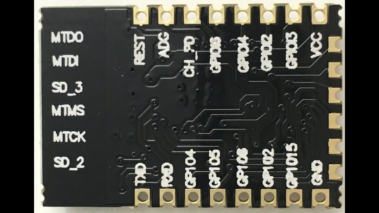
![Programando para o ESP8266 na IDE do Arduino e controlando um LED pela Internet [ESP8266 #02]](https://i.ytimg.com/vi_webp/Xcg8fAQ49Uw/maxresdefault.webp)














![Płytki drukowane [RS Elektronika] #42](https://i.ytimg.com/vi_webp/BS7Vb10GBh8/maxresdefault.webp)
This video provides a comprehensive tutorial on KiCad 8 PCB design, demonstrating the complete workflow from schematic creation to PCB manufacturing. The tutorial covers adding symbols and footprints, wiring components, assigning physical footprints, creating PCB layouts, routing traces, generating Gerber files, and uploading to manufacturers. The project demonstrates designing a Wemos D1 Mini prototyping shield with multiple stacked modules, pin headers, screw terminals, an LED, and a reset button.
Complete KiCad 8 PCB Design Tutorial from Schematic to Gerber Files
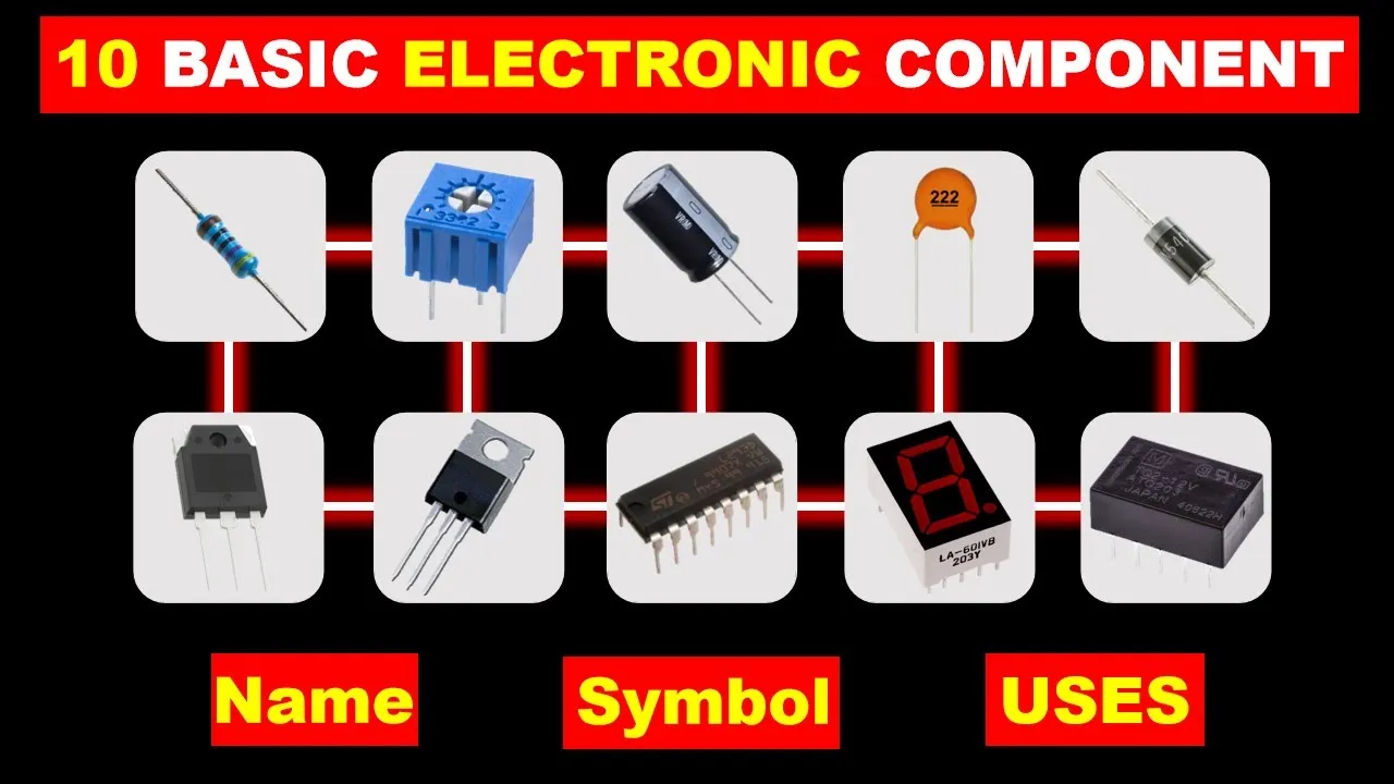
Added:Basic electronics theory, including the function of passive components (resistors, capacitors) and voltage regulators.
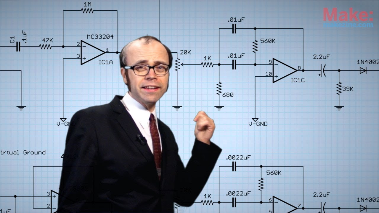
Understanding of schematic diagrams, electrical symbols, and how nets connect electronic components.
Fundamental concepts of microcontrollers, specifically the ESP8266 pin configuration, power constraints, and boot modes.
An introduction to physical PCB terminology, including footprints, traces, vias, silkscreen, and solder mask layers.
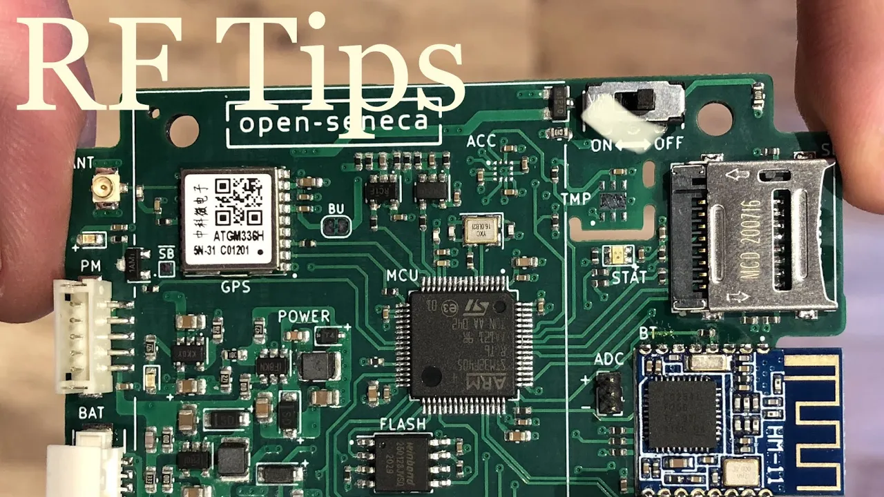
Advanced RF and high-speed PCB design principles, focusing on antenna trace routing and impedance matching for wireless modules.
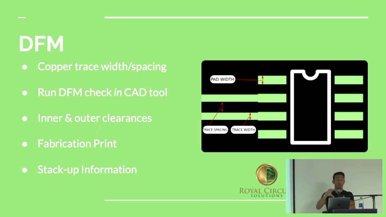
Design for Manufacturing (DFM) and Design for Assembly (DFA) protocols, including preparing Bill of Materials (BOM) and Centroid files.
Multi-layer PCB layout strategies (4+ layers) utilizing dedicated power and ground planes to minimize electromagnetic interference (EMI).
Thermal management techniques in PCB design to handle heat dissipation from active components and voltage regulators.
115.8K views2.6Klikes44:57Original Release: 2024-06-11
hello everybody I hope you're having a fantastic day and I hope that you are ready to learn we are going to learn kead today in one video and we're going to start from designing a schematic to choosing the footprints to putting those footprints on a PCB to exporting the PCB to Gerber files generating a 3D view of it sending it up the PCB way to get it manufactured and setting up a shared project so that you can get commission off the PCB that you Des designed how awesome is that so let's talk about what we're going to build the wias D1 mini is a little microcontroller that has Wi-Fi and some pins and stuff like that and the idea of it is that you can stack these other shields on top of it as tall as you want to add additional functionality so the problem comes in if you want to do something like this RGB LED you can't really stack the relay on top of it because it will block the LED and if you try to stack it the other way it won't fit and so the idea is that we're going to take this wias and we're still going to be able to stack stuff on top of it but we're also going to be able to stack stuff here and here and here which means that we can take our wios and add an LED and a relay and even another custom PCB that I made on kead and then to add a little bit more functionality we're going to add some extra pin headers for prototyping and some pin headers next to these so that we can have uh more things plugged into this board itself we're going to add some of these cool screw terminals so that we can do prototyping without having to make those special Dupont wires and we'll be able to basically do anything we want with the wias D1 mini in fact if we want to we can even add a Proto Shield to our Proto Shield which is just wild but of course we need to thank the sponsor of this video PCB way cuz thanks to them I designed this and this and this and this and this and all kinds of other things that make my life better and so I excited to partner with PCB way on this video although you will be able to take the files that we designed here and take them to any PCB manufacturer of your choice PCB way is truly my choice they're the ones that I use for my commercial projects they're the ones I use for my personal projects and it's because I love them they make great boards quickly at a great price so we're going to talk about them throughout the video go ahead download kycad version 8 and let's get started all right so once you have key CAD installed the first thing you're going to do is make a new project to we're going to go to file and new and then in my case I'm going to put it in my another maker folder just so that you guys can have this when we're done I'm going to right click new folder and it's going to hang up a little bit probably here but um so we're just going to call this key CAD 8 all right and then once we create the folder going to double click it and then I'm going to call the project key CAD 8 so now you have a new project and the first thing we're going to do is we're going to make a schematic so essentially just to kind of walk you through the process we're going to make a schematic that's going to show us electrically how the project is connected we're not worried about where parts are or anything like that and then the second thing we're going to do is we're going to identify the parts with what we call Footprints then once we're done with the schematic we're going to take everything and put it over onto the actual circuit board and then we're going to decide exactly how we want the board laid out now since the goal of this video is to get you up and running quickly I'm not going to spend a lot of time trying to make things super neat here if if you are doing this for yourself and it's a hobby I encourage you to take your time and enjoy the process now the first thing we're going to do is we are going to go over here to add a symbol and a symbol is kind of a good word for a part um as you can see here I've already filtered where I found out that there is a weas D1 mini on here and uh just to show you if there wasn't a wias footprint then honestly what you could do is just count the number of pins here and um just use pin headers we're going to be using pin headers in a minute so I'll come back to that but in this case we're going to want a weas D1 mini and we want to show that one of those is going on the board now if you'll notice this looks nothing like a weas D1 mini it is just a uh representation of the board but we're not actually seeing you know the outline of it and we're actually going to want to show four of those because we're going to have a um you know all of our breakout stuff so we're going to put four of them here as you can see I'm not worried about being too neat we're going to talk a little bit about moving around the interface uh I'm using a mouse with a mouse wheel and I recommend that you do the same so as I scroll the mouse wheel in and out you can see that I'm zooming in and out uh if I click and if I click the right Mouse button I'm moving the entire unit around and uh yeah those are the main things you need to know so we're going to Center on that now and I'm going to right click to drag this thing up a little bit I think what I'm going to do is spread these out a little bit so I'm just going to highlight the whole thing and drag and move let's get them down cuz we're going to want some space on top and bottom here so I'm going to drag these down here we're not going to worry about being too neat but we'll get these around here highlight the whole thing move it down and there we go so the goal of this project is not to just put four wias D1 Minis on one board we want to add some pin headers to the left and the right so that we can tap into them we want to add some places for power and ground so that we can tap into that we want to add some screw terminals for easy prototyping maybe an LED and a push button uh yeah we got things that we want to so in order to do that we need to add symbols now the first thing we're going to start off with is a bunch of pin headers that we can interact with those are pretty easy so what we're going to do is we're going to come over here to the symbol thing and all of the headers are under con uh they're all connectors but usually what I do is I think about do I want one row or two rows and then how many pins do I want so if I want a 40 pin connector which I don't then I would do 2x 40 and that's going to give us um a two row by 40 connector you can see I use my mouse wheel to scroll in and out but in our case since each side of the wiase has eight pins in it then we want a uh 1x08 not just 1 by8 we want 1 by 08 connector and so we're going to go ahead and grab that and we're going to put that in here and then we're going to want a couple of those so let's say um we'll keep it simple we're going to do one for each side of the we Mouse and then we're going to do one for each of the screw terminals so what I'm do is I'm going to copy this and I'm going to paste it before we go any further um if you look at the wios the pins aren't in order when you're looking at the actual board and so what I want to do is I don't want to mix up the left and right side so I'm always going to look at it that when the USB is down uh that's going to tell me left and right so we'll show you that when we get to the board but what I'm going to do is I'm going to just call this um I'm going to put an L there so I know that that's the left side and I'm going to put an R here so that I know that's the right side all I did was double click this when I had the pointer selected and I was able to put some uh you know some designations in there so we're going to copy this and I'm going to do one more for the screw headers and I didn't want to forget which one was left and right so um and now that I've done that I can actually come over here and take this one and put it over there with the other right one and I can take this one and put it over here with the other left one now um again this will make more sense as we're doing it but uh we're going to go ahead and add some more headers for 5V 3.3 volts and ground so let's do this let's come in here and let's say we want five pin headers so we're going to do 1 by 05 and then we're going to get this in here and we're going to put let's put these up top since most of the stuff is up top um so I'm going to do three of those and now we're going to do the same thing here so we don't forget what it is is you're going to make sure you switch back to your pointer you're going to double click this and I'm just going to put a g there and I'm going to put a 3.3 here I'll just put a V and I'll put a now there are other ways to label this stuff um and other people may like their way better but I do this and I tend to not mix things up when I do it this way so this is how I do it so although we have some more components to add I think it'd be good if we started connecting things together so that you can see a little bit about what we're doing uh the first thing I noticed is that on the Wii over here we have the 5vt is on the left and the 3vt is on the right and I did it the opposite way on my headers and there's no reason you can't do it that way but I'm going to move this around so that um you know it's just a little bit less messy on the wires and so we're going to do some wiring now if you notice if I click on just this it's just going to move the label so a lot of lot of times you'll see me draw a complete outline around it if you click the right spot it'll select the whole thing but if you have Space drawing the whole outline is great so what we want to do is we want to start making the electrical connections and as you can see over here I'm hovering on add a wire so what I want to do it tells me here that this is the 3v3 connection so I want to make a set of connected headers where no matter what pin you plug into you're getting 3v3 so what I'm going to do is I'm going to click and draw and then over here I'm going to go to pin five and this connected electrically um the 3v3 line on the header to this one now these aren't connected by default so I need to come down here and just draw a line and connect them all together and you can see that wherever two things Bridge you get one of these Green Dots which can be really helpful because sometimes you may not um mean to connect them so we can do the opposite here we can come straight down here through the 5 volts and then we can click on this and come down here and as you can see it's kind of smart about the way it does things now if you were really being anal you would want these lines to have the angle at the same spot I'm trying to get this done quickly for you so I'm not going to worry too much about that now the ground we want to do the same thing we want to come over here click it and then come up to the ground and then we want to connect all of these ground pins together and so that has given us um breakouts for this stuff which is super simple like it's not that complicated which is why we're learning this quickly so I brought up a photo from the most excellent random nerd tutorials and uh we're going to use that kind of as our guide as you can see here we've got pins that are in nowhere near the same order as they are in the diagram that you have up top and so what we want to do is we want to make sure that when we put a set of pin headers parallel to this that the wiring is in the same place so the first thing I'm going to do is I'm going to make a couple of notes on those pin headers um so I'm going to come over here and I'm going to select text I'm not going to get too complicated but I'm just going to come in here and just put like two letter designations for um each of these things and I'll type these out and I'll show you what I'm talking about so once I've actually typed out the labels uh if I'm on the pointer over here I can double click them again if edit them if I need to you can see I chose 38 Point font and all that good stuff so what I'm going to do is uh I'm going to take this I'm going to click on one I'm going to hit R and that's going to allow me to rotate this so I'm going to take the left one and put it over here and then I've got a second left header so I'm going to crl c contrl v that and then I'm going to do the same thing on the right header and contrl c contrl v and there we go so now what we need to do is connect the stuff all up to the wios so this is going to get messy and I'm not even going to try to be neat in a quick tutorial but like I said if you want to take the time to be neat you probably should um first thing we want to do is make sure that these headers are parallel to each other so we're just going to connect them together like so and continue that the whole way through so here's a top tip for you although there's a setting down here called The Grid um I highly encourage you not to mess with that so much I think you can go down to 25 Ms but basically by keeping everything on the big existing grid everything will snap together a little bit better and these things will all connect so that's just a pro tip don't mess with that until you're ready to get into expert mode um but the next thing now these pin headers are only connected to each other so the left is connected to left the right is connected to the right but nothing is actually connected to the wios and so it's time to do that so what we're going to do is we are going to go up to the wios here and we're going to find the TX pin and this is where you can spend all sorts of time trying to be neat and all that kind of stuff but basically you're going to come around here and make your wire connections and you'll see that you get the dot there when you've made the success connection and the way it works in this world is that things just don't line up the way you want them to so there's going to be a bunch of crossover and stuff like that but essentially what we need to do is to connect each of these pins to its partner down here so we're going to do that it's going to take a little while uh just go through and connect everything to everything [Music] now I think I'm going to jump back in here and show you that when I made this last connection I came up too close here and I accidentally connected to the two pin so I don't want to do that um so to get rid of one of these things all you have to do is click on the uh pointer and click on the wire we're going to delete that and then we're going to delete the connection between the two um so I need to get on that little tiny wire right there all right as you can see these cross over but because they don't have a DOT they're not electrically connected so we're going to come over here one more time last wire on this side and we're going to come up come out here and then I'll Zoom back [Music] out okay so I'm going to want to double check that but um essentially every pin on the first wios is connected to these headers down here so that's job done so as you can see we have a pretty full section over here and what I think I'm going to do is I'm going to try to spread this out a little bit so we're going to come over here to file and page settings and to be honest it's not like that we're ever going to print this out so we can make this as big as we want so I'm going to make an a Zer and give myself plenty of space to mess with now if you watched while I was routing those wires it did look like still the bulk of the right side connectors went on the right side and then most of the ones on the left were on the left so what I think I'm going to do is I'm actually going to move these down and put these on top of each other like this and I'll show you what we're going to do so I'm going to use my scroll wheel to zoom in and I think what we're going to do is we're just going to go ahead and connect all the other ones together down here so the two will get connected to the two um so we're just going to go ahead and basically do this and I'm going to leave myself some space for some angles but we're going to come in here and do like that and then we're going to click this one here and we're going to try to make that mate up with the other wire like this and these things are all just paralleled together it's just a bunch of shields so we're going to click that and so we're going to go through the whole thing and essentially jumper the two to the two the three to the three the four to the four that kind of thing [Music] all right so that is that half done now we're going to go around and do the [Music] top so if I zoom out on our schematic you'll see that basically what we have here is we have these three Shields are all connected to each other this is connected to the pin headers but these are not connected to this and so what we want to do now is we want to make the connections between the three headers and their respective uh pins on the shields over here so I'm going to go ahead and connect 2 three and four to one and uh I've been debating about how to do that I think I'm just going to go straight from the wios so I'm going to come down here and then connect like that so that's going to be a whole bunch of other connections just straight through and I want to do that quickly all right so it's not the neatest thing I've ever built but it is all connected as far as I can tell we're going to check that in just a moment I do feel like I would be remiss if we didn't add a couple of just passive components to this thing so that you could get an idea of how that works so I think the first thing we're going to do is we're going to build in a uh an LED so that we can tell if the power is on and then I think the other thing we should do is add a reset button there's a reset button on the actual um wias but let's go ahead and put an external reset button so what we're going to do is we're going to come in here to the symbol editor and we are going to look for LED and we're just going to add a simple led to it and we'll just stick that out here to the side doesn't really matter uh let's do you know maybe we do it up here let's do it up here let's see we got five yeah let's add that up here um and then let's go ahead and add a current limiting resistor for that led so we're going to just start typing in resistor and we're going to add a resistor and then we know that's going to have to go right here so I'm just going to hit R to rotate it and we're going to stick it there and then um the next thing we're going to do is we're going to add a button and so I don't remember what the symbol is for that so I think it's just push button s SW push uh I think that's going to be it so we're just going to add this standard push button and we'll stick that where's the reset pin we'll stick that right here so what we're going to do is we're going to send power um from 5 volts through the current limiting resistor out the LED and the ground so what I'm going to do is I'm actually just going to stick this right here so I'm going to drag this over and we're going to make sure it connects but yep there we go and so then since we're here we can go ahead and take this and just grab that and then anytime there's power to this thing that led is going to light up now the next thing we want to do is um the way the wias works is if you push a button between reset and ground then um it will reboot the board so what we're going to do just for clarity we're going to come out here and we're going to come down to the reset pin and then we're going to come up here and go to ground which is actually right here so I'll just click on that and then that is our push button so that completes the stuff that we're adding to the board but it doesn't exactly tell us what we're adding to the board in other words we don't know if this is a 3mm led a 5mm LED if it's one of those giant 100 watt LEDs we have no idea and the way that we fix all that is we run the footprint assignment tool and what you have here this can get a little bit messy but what you have here is um this is the designation that we have on the board so when you look at the you know U so this is U1 wios D1 mini um so basically what you're doing is we're assigning these four are weas D1 minis now they're really it's really a a weos and then three Shields but that's fine so at this point everything is laid out but we haven't actually told the schematic what is in these places like in other words we know there's an LED here but we don't know what size the LED is we know there's a resistor but we don't know the size of the resistor all that kind of stuff so what we're going to do is we're going to come up here and we're going to run the footprint assignment tool so in order to read this um on the left side you have the component designation so like U1 is a microcontroller here so uh we have U1 U2 u3 all those are here the LED would be D1 stuff like that so um we have those designations but most of these the right side isn't filled out which means that we haven't told it actually what kind of that component is here so if we click on the LED because it's first we're going to go over here and um we're going to find the LED library and we want to do through hole not SMD these are surface mount so we're going to go to through hole and then over here on the right you can see the various sizes of LEDs so we have 5 mm LEDs we're going to use the smaller 3mm LED so I'm going to double click that and you'll see that that gets assigned over here on the right now these connectors work just like they did when we were doing this side um for this thing we want a pin header so we're going to go to uh connector pin header 2.54 mm which is the standard size and then we want a uh 1 by 8 so we want to find 1x8 and you'll see that they are that they are listed as um horizontal vertical or vertical SMD so we want vertical because we want the pin headers that stand straight up so because we need a couple of these um we can copy this and paste this here and that will get us connectors one and two now for three and four those are the chunky uh screw terminals so that would be a connector what would they call that that's a connector I think it's r& D it is terminal block R&D and the ones I have are 5 mm apart so we want to grab the R&D 1x5 5 mm horizontal and so we're going to click on this and then 1X 5 mm horizontal and we have a second one of those so we're going to copy and paste next we have three of these 1x5 standard pin headers so we're going to come back here to 2.54 mm and we're going to find the 1.5 vertical vertical so we're going to select that 15 vertical there we go now we're going to copy this because we have three of those now for the resistor we're going to use a standard resistor these are a little weird to put in there you kind of have to know the size uh but we're going to use a through through hole resistor and you can choose to mount it horizontally which is like laying on the board or vertically we're going to mount it horizontally and what we want to find is um when you look at them a lot of these are vertical so we don't want the absolute smallest one for the tiny resistor but we're going to go up just a little bit bigger to give us some extra room so we're going to take the this one looks good and we'll get a chance to see it on the board in just a moment um just trust me on that size there the last one we need is one of these buttons and so we're going to find the button library and this is through hole as well and uh we can clear out that search term there and we want tactile buttons so we want the standard 6 mm which you may not know that's the standard but that is the standard for 6 mm tactile push buttons so when we're done we can hit save now there's this whole concept of Nets and we're not going to really spend a lot of time talking about that in this video they can be super helpful for doing all your wiring and things like that um but we are going to add one symbol to the board that's a little different so we're going to come over here to the power symbol and we are going to add just a ground symbol um right here to this ground connector right here to let us know um to let kead know where the ground is going um we'll see that in a little bit but just trust me on that one the other thing I wanted to show you while we're in here is in the event that you have a pin on something that you don't want connected to anything um you need to come in here with this little symbol here and Mark that pin as not connected and that will tell kead that you've done that intentionally um we're not going to do that here but I just wanted to let you know cuz you could run into some errors um if you didn't know about that so we're going to go ahead and connect this back and there we go the next thing we're going to do kecat is probably going to throw a bunch of fits on it I haven't tried it yet but um we're going to run the electrical rules Checker and the main reason why we want to run this is to make sure that nothing is disconnected it's really easy to get in there and miss a connection or something like that um now the fact is it's most likely going to think that we have four wises and that we're sending power to power and ground to ground doing all kinds of weird stuff like that so we're going to be ignoring some errors that we see but we're going to still run the electrical rules Checker and make sure that it doesn't say that nothing is disconnected or there's something else weird going on so let's click that and run this and you can see we get 14 errors I'm guessing yes it's saying input Power Pin not driven by any output power pins it doesn't know what I'm doing with this board so I'm not going to spend a lot of time worrying about that but what I am looking for is is there anything disconnected uh and there isn't there aren't any errors about anything that is disconnected on the board so I'm going to close this and we're going to move on all right so we are finally getting to the exciting part we're about to make a PCB so we're going to save our work and we're going to go here just to make sure that all of our letters and everything are right we're going to come down here and hit tools and annotate schematic there probably won't be anything to do there but we're just going to let it do that and then finally we're going to go to tools and switch to PCB editor and now we have a screen that looks some somewhat familiar with similar tools but different because this is for laying out the circuit board so what we're going to do is we're going to come up here to tools and update PCB from schematic and hit update PCB and it is going to just drop all of our components here on the board and we're just going to set them right here in the center uh now the most fun thing to do at this point is to go to view and 3D viewer and you can see all of the parts on the board now this is kind of a bad representation cuz it looks like there's four wios boards but really there's only uh one and three Shields but either way um we get a representation of what all these parts look like so you can see your resistor and your LED and your button and all that kind of stuff there's not 3D models for every single part but you get the idea so we are going to come back to this in just a minute but um first of all we are going to close it so the first thing we're going to be concerned about is the cost of the board and most PCB manufacturers including PCB way give give you the best deal if you keep your board below 100 mm by 100 mm so what we're going to do is we're going to come over here to Edge cuts which is going to define the outside of the board and we're going to grab this rectangle tool so as I begin drawing the rectangle you can see I just click and let go you can see the size showing up and I want to make one that is 99 mm by 99 MIM and this will kind of give us the maximum amount of area that we have to play with I guess we go 99.5 and that gives us the maximum amount of area that we can play with now the next thing I'm going to do is um click on the arrow and I'm going to right click on this board and I'm going to hit lock um and this will stop me from dragging the board around or accidentally resizing it and making it bigger that would be tragic cuz I think that I'm in the right size and I'm not and the other thing you want to do is you want to down here on the selection filter make sure that you have locked items checked and that will allow you to rightclick something and unlock it should you need to Okay so let me explain what we're looking at we have all the components that are in your project dropped on this thing and when you click on one either by clicking on it or by highlighting the whole thing you can see that it has these blue lines now these blue lines are not actually your electrical connections but they are where you will need to Route wires in the future so it's important that you Orient these connectors in ways that make running the wires efficient so if I were to flip this upside down you would see that that all these wires would have to crisscross and crisscrossing wires are bad uh not that you can't do it but it just makes everything more complicated so what you want to do is you want to start placing these things on your board in a relatively intelligent manner so we're just going to start kind of working them over here um and we're going to just start getting them in a rough idea of where they're supposed to go now um thanks to gadget reboot for reminding me uh this wios has a USB connector on the front so I do want um the actual wias to be down here in the lower left so that when you're running the cable you're not running it all the way across the board so um we're going to go ahead and take care of that too uh while we're doing this so we're going to drag this down here and then we're going to drag this one down here so as you can see we have uh the real wios in the lower left then you've got Shield one Shield two Shield three it doesn't really matter what what order these shields are in what we're going to do next is try to get these things to be a little bit aligned with each other so I want to make sure that vertically these two are the same height so I'm going to highlight them and I'm going to right click them and I'm going to hit align distribute and I want to align these uh on this same axis right here and then I'm going to do the same thing here we're going to align these two on the same horizontal axis so align distribute right there you see it bumped that one down now I want to make sure that these two are on top of each other so I'm going to right click this and Aline and we're going to pick this horizontal Center and that knock those in line and then we're going to do this one right click it and that put those in line totally didn't know how to do this when I first started so that's uh really helpful um so what we're going to do next is we are going to come over and grab these other parts and just get them a little closer so that we can deal with them now as you can see here we have the right header so I'm going to do the same thing I did before where I hit the r to rotate it and you can see that does kind of crisscross it over and I think we want it that way anyway so we're going to put uh j4 at the top because that's the right one and then we're going to put I'm going to leave some room here I'll show you why in a second I'm going to rotate this one and we're going to put j3 right down there this could have been one header totally but I didn't um now the next thing we have is our headers for the left and right side of the primary wias so we're going to put a set of headers here and we're going to put the other side here and again we're making sure that they are uh electrically in some kind of order that makes sense and I guess now what we can do is do this and we'll see about aligning this this way uh align to Vertical Center yeah so that just shifted them so that they're all exactly the same um and then now we've got the these power ones that can go wherever we have this resistor that I kind of have a plan for and uh everything else can wait just a moment now for some reason it is kind of hard to visualize exactly what's going on here so you can always go back to the 3D viewer and fire that up and get an idea for what your board looks like in real life and um I feel like I have plenty of space between these I'm going to probably slide them over use some of this space up for something and I kind of want as much space at the top as I can get so uh I'm going to close this and I'm going to grab these and now I'm going to hit the m key so I can move it with just the arrow keys and so I'm going to slide that over so that they get closer to each other and I get some of this space back over here and we're going to take these three things here these three headers and we're going to grab those and bring them over here so we'll kind of separate those out and we will use this alignment tool to right click and we'll distribute them and align them so we're going to distribute them vertically and then we're going to rightclick align and we will Center them on that axis yeah thinking about it we have a ton of space over here uh let's go ahead and grab this and put it over here I'll rotate it so it takes up a little bit less space and uh we're going to move this over here we'll do something with it in a little bit but that actually puts it closer to the reset set pin um we're going to want to make sure and this is really easy to not do we're going to make sure that we are on the silk screen layer and then we're going to hit this text thing and we want to um type in weas D1 mini right here and we want to put silk screen layers uh places that we're going to be able to see them so that we know what goes where so I can go ahead and copy that and uh we're going to there's a lot of snapping going on here we're going to go ahe and paste that not perfect but good enough for our purposes um now we want to look at the board again because one of the things that can distract you a little bit is that you see labels on here and that may not be what actually shows up on the board so when you do the 3D viewer you kind of get an idea of what will be finally um rendered so we have Shield two Shield three down here we have uh Shield one and the weas D1 mini and so um you know but we are missing labels on all of this stuff over here we don't know what any of these things do so I'm going to go ahead and add some silk screen to those things so that we can see what they do okay so I sort of nudged things around a little bit let's take another look at it in here um again you can spend as much time on this as you want uh just click and drag around take a look at everything see if it makes kind of sense I know we've got this button hanging out over here maybe that button should go a little bit lower um I don't have a label on the button saying what it does I don't have labels on these things saying what they do so um still have a little bit more work to do let's get back to that um now what I want to do is I want to be a little bit stupid and I want to add uh some giant text up at the top so let me do that all right so I think that's ridiculous enough so I'm going to come over here drag my uh resistor and my LED over here and we're going to get these in the right position like so and then we'll slide the resistor down and then we'll put the LED on top I think honestly this font could be a little taller um we could use the extra bowl but I think that's going to give us some issues so I'm going to make this nine height so it'll be a little skinnier yeah a little cheesy but I like it all right so I'm not going to waste too much of your time on that kind of thing um everything looks about like I'm expecting again you make your board the way you want to make your board uh the only thing is we haven't talked about the back of the board and so uh what I'm going to do over here on the silk screen I'm going to click the back one and then when I put my text on there um you're going to see that it's all going to be in Reverse so if I go to the 3D viewer when I rotate this around you can see project by another maker and it has my GitHub but when you're actually looking at it from the PCB it's kind of funny you're looking at it through the back so you see the reverse side of it all right if you've made it this far you are so close to having your first PCB done uh what we're going to do is we are going to Route the wiring so that's right we actually have to route the wiring and the way this works is when you go over here to the wire tool and you click on something then basically everything that is not connected to this uh dims out and you can see like I can't connect to this pin because it's not supposed to um but this thing is going to try to Route these wires all over the place and that's great with the exception of the fact that wires cannot cross over other wires on the same side of the board so the issue is that you want to do this as efficiently as possible and um I do encourage you to route a lot of these by hand and to learn this process cuz it is kind of fun um but we're going to do it the easy way since this is your first PCB so I'm going to tell you to install two plugins we're going to come to the plug-in manager and you're going to type in free and you're going to get free routing and go ahead and click that and then the other thing you're going to want to do probably is do PCB way um the sponsor of this video and I'm not just saying that cuz the sponsor of this video they really do make this easier so go ahead and click that and um once you're done hit apply pending changes and then come on back it'll take a minute but come on back so people who design a whole bunch of pcbs probably aren't going to like that I'm going to show you this but to be honest it's probably the better way to learn uh at least on your first PCB so we're going to click on this free routing button and it's going to open up something on the next page that you're not going to be able to see for a second but you can see once I hit start that this thing goes through here and automatically routes these traces for you now there's a lot of settings where you can choose the width of these things and how close uh that a track can get to one of these pads and all that kind of stuff and you may want to mess around with that and in fact I'm going to link you to a video with a lot more information on that subject but for the most part you can just let this thing go and see what happens so there you have it all your tracks are routed in the event that you don't like the way that it did it or you need to make some kind of changes you can come in here to edit and Global deletions and click tracks and Vias hit okay and it will take them all away and you can just do it again so there are two final steps that we need to do in the board creation process we need to fill in these extra zones around here by doing that we will make the board easier to manufacture we will provide better heat syncing we could provide better electromagnetic and interference protection all that kind of stuff we want to have as much copper in the board as possible so what we're going to do is we're going to click this ad filled Zone and you're going to go somewhere outside the board and you're going to click once now that will give us some options and we want to fill both the top and bottom layer of the board now we could just create an island and put a bunch of copper in there for the sake of having copper and there's nothing really wrong with that but what we're going to do is we're going to tie this into ground so that all this copper gets tied together so once we made that decision we can go ahead and hit okay and then we're going to continue doing the outline around the board it doesn't really matter if you're neat you can go like this whatever just get outside the board and then make sure sure that you close your shape by double clicking so once we do that um the last thing we need to do is to run the design rules Checker and this is going to take a look at all the connections on the board and make sure that we are not having any issues so we're going to click that button and I'm going to run the DRC and you will see that we have no errors which is good we do have five warnings which we'll take a look at those in a minute uh if you have any errors you might need to get some text support on the key CAD Discord but for the most part these go pretty well we are in the home stretch so let's go ahead and click on warning so that we can take a look at these and you'll notice that if we click on a warning it somewhat tries to Center us on it so we can see here that yep that is off the edge of the board I'm just going to click on that and we'll select that reference and we're going to drag that inside here now this will get covered up when a component is on the board there but who cares um let's do the next one j3 yep same issue there so we're going to grab these and get them on the board don't want our silk screen to be all over the floor um so we got that there one last move there that takes care of those two will'll run the design Checker again and we're down to three so let's take a look here we have a clipped by solder mask oh yeah they're all right in that area so we've got one two three with the silk screen overlap now this first one here I can see an R1 uh that accidentally got drug into the wrong place so we're going to move that down there and we'll run that DRC one more time and see that right now we have none yeah okay so this one was overlapping a couple other ones and that was giving us all three of our errors so we are done so I'm going to show you both the manual way and the automated way to deal with the Gerber files which are what you're trying to get out of all this stuff so that you can have it manufactured at a PCB manufacturer like PCB way so what we're going to do is we're going to save our project and we're going to hit this thing that looks like a printer but different it's a plotter we're going to click on that and we are going to come up here to our path and what I like to do on something like this is I like to make my own folder in here we're going to call this key CAD 8 video Gerbers and once we create that then we're going to go ahead and double click on it to enter it and select it and we're going to say yes that we want to use it relative which is a little weird terminology but that's how it goes uh so now what we're going to do is we're going to generate our drill files and generate drill files and hit close and then we're going to plot and we have Gerber files you can close so as you can see in the folder I have a whole bunch of files my drill files and Gerber files and all you need to do is rightclick that and zip it up and we're going to have a set of Gerber files that we can send to a PCB manufacturer my PCB manufacturer of choice is PCB way not only because they sponsor the channel but because I'm a customer on my own as you can see I've got four items in the cart right now so what we're going to do is we're going to go to PCB instant quote and we're going to Quick order PCB and then we're going to add our Gerber file and hit open now as you can see here five boards is five bucks but if you come over here to this and you click it you'll actually be able to get 10 boards for five bucks because we kept it under 100 mm and so um now if you have multiple items you can combine shipping and if you want to pay even a little bit less and you're not in a hurry you can come out down here to global standard shipping and get it for you know almost a third of the price for shipping so uh anyway once you're done you have it the way you want it you can choose board color if you want red boards if you want a different color solder mask whatever you want and then you hit save to cart make sure that you don't have anything illegal in there and save it if you think that's too complicated you can come over here to the plugin and content manager on the main key CAD screen search for PCB and install the PCB way key CAD plugin and all you have to do is come up here and click the PCB way button and that will pretty much take you straight there it brings up the website with your Gerbers already loaded you can just choose your quantity and you are Off to the Races so this is not a commercial one of my absolute favorite parts of PCB way is their shared projects not only getting them from other people but I love actually putting my own on there and you get really good commission that you can use to buy pcbs so basically all of your pcbs can be free if you wind up putting your projects up here on their shared project there is a create project button in the upper right hand corner and all you need to do is fill out a title give it a couple of categories and a basic pitch and then we'll move on so I gave it a title the weos D1 Maxi prototyping shield and gave it a couple of categories how my elevator pitch so from there I just need to upload my Gerber files and I'm going to put a picture in here I'll get some more pictures once I get the boards in my hand and then one of the cool things is that you can put the bill of materials down here and you can actually use your own affiliate links so if you're part of an eBay or Amazon or AliExpress affiliate link thing people who even just look at the board can use your links to buy stuff and you can get credit for that as well so you can do something like this where you say you know explain what the board does you give your affiliate links and then you say it's an Arduino esp8266 Hardware give it some keyword things and then hit submit and your project will be online so I want to thank you guys for sticking with me through the video I want to thank PCB way for sponsoring the video I want to thank kead for the awesome software I will have some links to some great resources for learning and getting support on kead I am not able to offer support for kead in the comments of this video but I do hope that you learn a lot and that this begins a lifetime journey of PCB design so hey thanks for watching and have a great day
Up Next
19:54
Homebrew SDR SSB Rig Part 2: Quadrature Phase Oscillator
@CharlieMorrisZL2CTM
7K views•2018-03-21

12:54
Triumph of Orthodoxy Icon: Byzantine Art & History Explained
@BenCallan
2.1K views•2024-08-06

9:49
FastAPI vs Flask vs Django: Choosing the Right Python Web Framework
@TechWithTim
302.5K views•2024-05-26

1:42
Game of Thrones Opening Credits: A Cinematic Analysis
@gameofthrones
46.3M views•2011-04-18
Related Study Plans & Knowledge Roadmaps
Structured learning paths in General & Interdisciplinary Studies
general-studies
Elevator Engineering: History, Physics & Cities
01From Hoists to Safety Brakes: The Dawn of Vertical Lift
02Hydraulic vs. Traction: The Engineering Physics of Elevators
03Modern Speed, Safety, and Algorithms
+ 2 more learning modules
12h5 modules
Explore Roadmap
general-studies
Rubber: Material Science, History & Geopolitics
01Origins of Natural Rubber & Mesoamerican History
02The Chemistry of Natural Rubber & Vulcanization
03The Geopolitics of the Rubber Boom & Colonization
+ 2 more learning modules
12h5 modules
Explore Roadmap
general-studies
Containerization: Evolution, Logistics & Trade
01Ancient Trade & Bulk Cargo: Amphorae to Barrels
02The Industrial Revolution & Cardboard Packaging
03The Containerization Revolution: Malcom McLean
+ 2 more learning modules
12h5 modules
Explore Roadmap
general-studies
Textile Tech: Evolution, Labor & Global Impact
01Pre-Industrial Textiles: Handloom & Cottage Industry
02Mechanization: The Spinning Jenny to the Power Loom
03The Factory System & Global Labor Transformation
+ 2 more learning modules
10h5 modules
Explore Roadmap