
![STM32 na Rejestrach | #1 Wprowadzenie do CMSIS | [POL]](https://i.ytimg.com/vi_webp/0Sy4g4xp4WU/maxresdefault.webp)

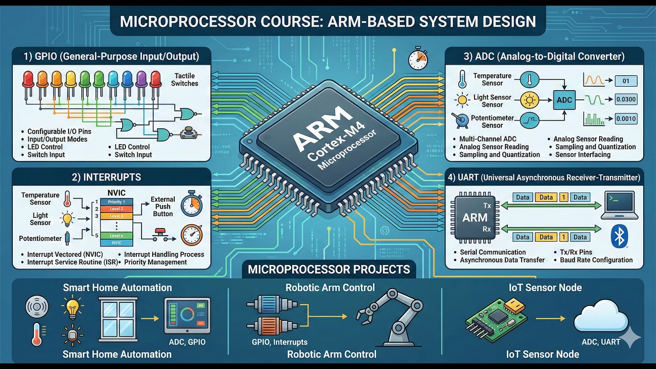
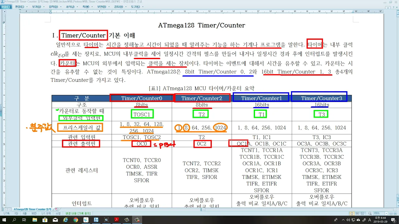

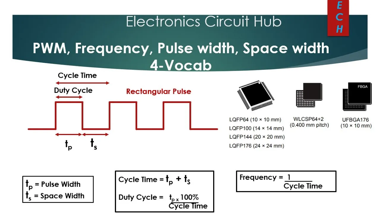






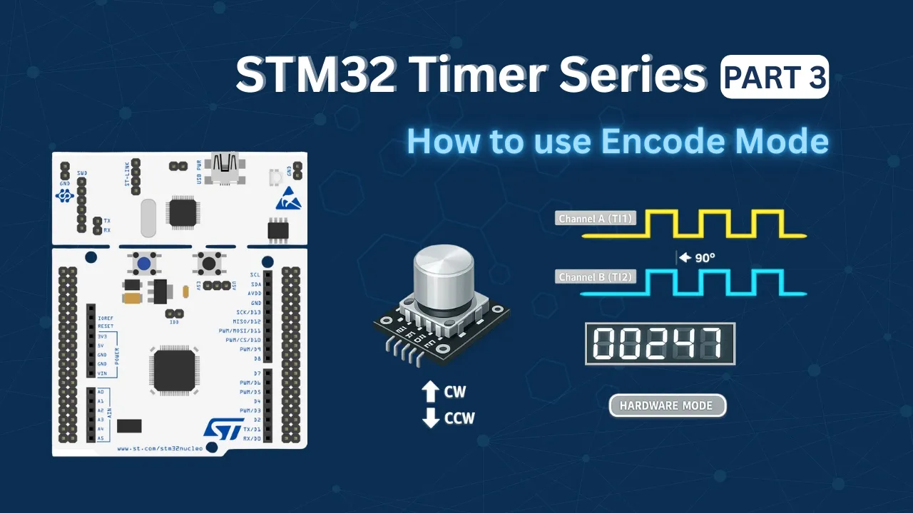






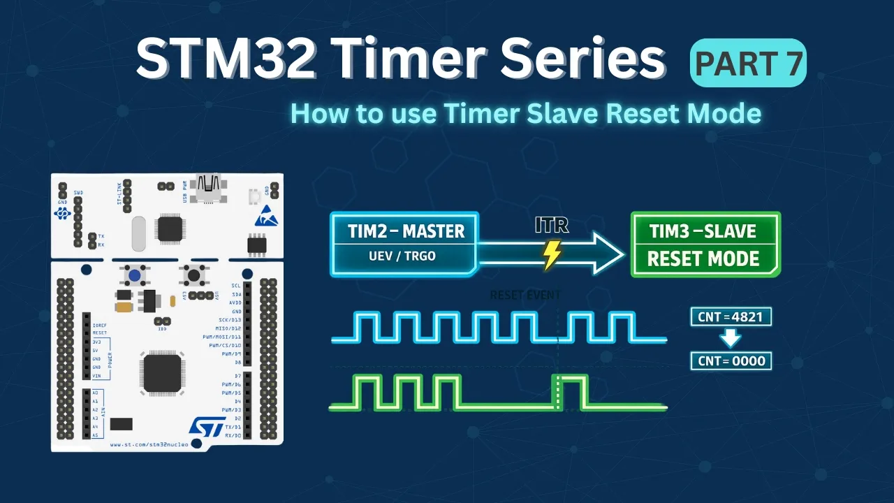


The STM32 timer peripheral input capture mode captures external signals by storing the counter value at the capture register when an edge detector detects a transition (rising or falling edge), while PWM input mode captures both rising and falling edges using two capture registers to calculate frequency, duty cycle, and time period of square wave signals.
STM32 Timer Input Capture: PWM Frequency and Duty Cycle Measurement
Added:Basic understanding of STM32 MCU architecture and register-level (bare-metal) C programming.
Fundamentals of hardware timers, including prescalers, auto-reload registers (ARR), and counter directions.
Core concepts of Pulse Width Modulation (PWM), including frequency, period, active-high/active-low polarities, and duty cycle.
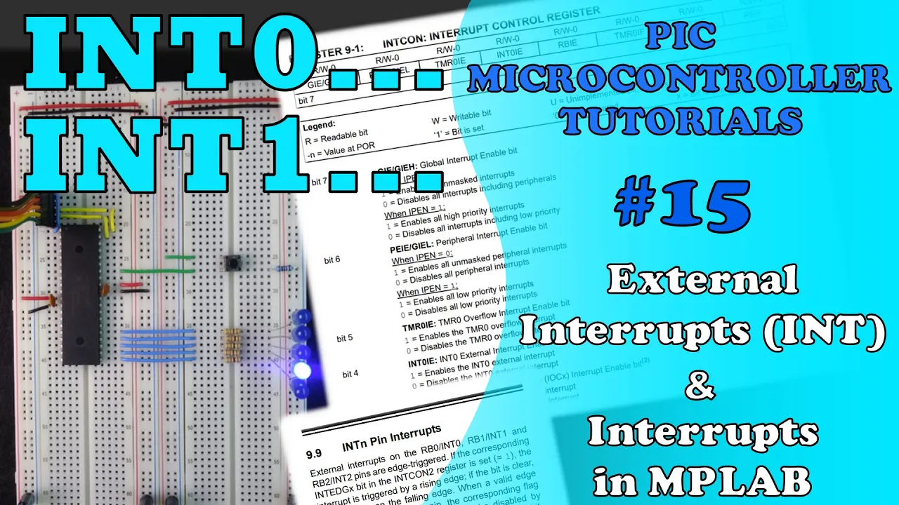
Familiarity with microcontroller interrupt handling and writing basic Interrupt Service Routines (ISRs).
Implementing Direct Memory Access (DMA) with input capture to measure high-frequency signals without CPU overhead.
Utilizing STM32 Timer Encoder Mode to interface with rotary encoders for velocity and position tracking.
Decoding complex sensor protocols (such as DHT11/DHT22 temperature sensors or infrared remote controls) using input capture pulse width analysis.
Mastering advanced timer synchronization techniques, including master/slave modes and triggering external peripherals.
1.3K views19likes10:48Original Release: 2022-05-27
so hello guys welcome back to channel get to bite once again it's been really very very long since i have come up to the channel and uploaded the content on the firmware development on microcontrollers so i have started with stm32 and then in between uploaded some of the introduction videos on texas instruments and the nordic controllers also but from now on i will be making a stick to one microcontroller and completing its peripherals and application codes and further outdoors so stm32 will be the series that i will be continuing with and i will make sure that my previous mistake is not repeated of being inconsistent so guys the reason behind my not being consistent is because i have been in i am in the final year of my b tech so i am finalizing all those things and also i am in finding the new job to start my professional career and i have a job as a firmware developer in nxp semiconductors so that will be separate video i will be making about my journey about what things to do and those things now in this video we will be concentrating on the firmware development on stm32 microcontrollers so now without wasting time now let's start with this video [Music] do [Music] so guys in this video we are going to start with the timer peripheral and in that diameter we are going to write the driver for the timer input capture mode that is so as to capture the out the external signal square signals of pwm waves like as you can see here is a logic analyzer i have attached the oscilloscope which is outputting the 10 kilo hertz of frequency so this frequency and this square wave is being will be fed to the microcontroller and microcontroller will be identifying the frequency the duty cycle the time the period and the time width so all these things can be done using the timer peripheral input capture mode so in this video we are going to start with that topic only we are going to write the timer peripheral driver okay like as you can see over here i have written the driver and i will just show you the values you can see over here frequencies approximately 10 000 duty cycle is 50 period it is showing what it is showing so that all things it's an output of the the external signal is of 10 hertz okay frequency 10 kilo hertz and almost my values are same over here so we are going to write the driver in bare metal coding using the timer peripheral okay so now let's start the now that's the agenda of that will be the agenda of the video now let's start first of all with the introduction to the input peripheral uh of the timers okay like what all registers are there over and what all things we have to taken care of how does input capture mode works and what all those things okay so now let's start with the input capture mode briefing in stm32 microcontrollers so guys now starting with the timer input capture let's just first start with understanding the basic thing about the block diagram of our general purpose timers so in the block diagram of stem 32 controllers general purpose timers you can see this area so this one this area left on the this side is for the timer input capture okay so here time x channel one time external to time x channel three time external four so what does this means at each timer in our estimated two controllers has four channels channel one channel two channel three channel four you can also see this if you will see the pin out so you can see there is names written as t4 c1 t4 c2 t4 c3 t4 c4 so this is timer for channel one two three four now on the each channel okay we can sample the signals these ti stands for external external input pins so as it's in an input capture mode so it would be having a pin that can would be a uh capturing on uh some input from external output so that's what t i here signifies for external input pane so external input with one for channel one external input pin two for channel two channel three and channel four these are just terminologies which you have to know for understanding the better things uh otherwise from the pin out you can directly see that which channel you are using timer for if you are using in which of its channel so timer for channel one is at the pin pb6 that is 42 pin number of this ic so pv6 will be uses timer input capture mode pin okay same if you are using channel 2 of timer 4 then that bit so correspondingly you can see and look out the things now uh as you if we move forward from this thing so time x channel 1 these are the four channels that will be outputting or inputting some uh signals like external signals at the ti one ti2 ti3 ti4 which which are nothing but just time f time x c x c y appearance and then comes our input filter and edge detector so what does this blocks do now these blocks will collect the uh in output signal okay and it will filter them and detect that which of its edge is being been detected whether it's high edge or low edge depending upon the high or low edge as corresponding some of the bits we have to set and configure it and then uh using the prescaler we the counter values at what interval when counter will be incrementing from zero to some value and then when and and as our as detector detects some lower highest then some uh counter value will be stored at capture or compare register in the case of input capture it would be capture register okay because comparison will be done in pwm mode uh when we are outputting some signal in case of input will be capturing that thing so capture register it would be named as and depending upon the pre-scaler our frequency and the frequencies at which the microcontroller can capture that would be uh dependent okay so i hope you got the basic idea what exactly how does this block diagram of input capture is now all the inner details i will tell you further okay so guys now starting with it so in our stm f103 there are two things in timer peripheral input capture input capture mode and the pwm input mode so now in this video we are just going to get a very basic overview that what are basically these two modes are and what is this and then the next video we will get into the implementations of these by the understanding the registers of these modes for the timer peripheral input capture mode so now in the input capture mode is a basic and simple one in which what happens is our value of the counter that is time x c and d logs the counter value at the capture register that is timex crx uh they it captures the car it locks the counter value time xc interval is log into these registers as in when the edge detector which i have told you in the previous block diagram you know in the block diagram of verify of timer or peripheral as detector detects the transition chain in the external signal so now in the input capture mode you can understand and see that there is only one channel of the timer that will be occupied for capturing the s detector transition states okay so now only either at the rising or or the falling edge of the external signal can be logged into the ccrx register now whereas in the pwm input mode what happens is one can identify the frequency duty cycle per time period and all such parameters how in this the external signal which is there which is pwm square signal it's rising edge and the falling edge both of these edges can be locked onto the timex ccr one cc rx register of ry registers so one resistor will be used to lock the rising edge and one register will be used to lock the uh falling edge and by that how one can calculate the digital signal frequency time period or duty cycle so that is the main difference between the input capture mode in which only uh one uh transition state of the external signal is captured and in this the both the rising and falling uh transition states of the signal can be captured which is used to help calculate the parameters of square signal so this is the basic difference as you can see this is a pwm input mode timer okay so this is my ti one is the uh yeah one more thing is that in pwm input mode if you can see there is involvement of the two channel registers but it doesn't mean that we are going to use two external pins we are going to use one external pill only and the one timer channel is directly connected to our external pin and another timer channel will be connected internally to that in external pin so that when the external pill higher the lower the like we can set its polarity that when the timer takes ti one high edge comes so first channel will lock the channel when it's uh falling edge will come so another channel will lock the weather so that's an and that's how one can calculate these values like as you can see time xcc r1 time xcr 2 not ti one is my square signal so it's falling edges rising it is directed so ic1 capture ic to capture reset so icon like that is cc r1 captures the data okay when ti one this edges come now when this edges come i see to capture them uh ic2 will capture the value and its counter value will be keep on increasing okay so that's in and that's how one can calculate the the frequency and also parameters of the signal so that is a basic difference between input capture mode and the pwm input mode now in the next video we will go into the register descriptions of these and we will understand that what all resistors are there and then we will start making a bare metal driver so that's it for now like the video subscribe the channel and press the bell icon to get notified for new videos and share it with your friends [Music]
Up Next

19:26
STM32 UART DMA with IDLE Line Interrupt for Variable Data Reception
@ControllersTech
76.3K views•2021-06-19
30:32
Ultrasonic Transducers: Resonant Frequency Measurement and Horn Design
@imajeenyus42
229.9K views•2017-02-22
54:16
Polymer Environmental Degradation: Mechanisms & Stabilization
@iit
1.8K views•2012-07-10
33:39
How a Student's Question Saved a NYC Skyscraper from Collapse
@veritasium
22.8M views•2025-04-26
Related Study Plans & Knowledge Roadmaps
Structured learning paths in Engineering
engineering
Building Acoustic Levitators: Physics & Arduino
01The Physics of Sound and Standing Waves
02Piezoelectric Transducers and H-Bridge Drivers
03Arduino Programming: Generating 40 kHz Signals
+ 2 more learning modules
14h5 modules
Explore Roadmap
engineering
Building Peltier Cloud Chambers: Particle Tracks
01Cosmic Rays & Cloud Chamber Physics
02Thermoelectric Cooling (TEC) Fundamentals
03Custom Liquid-Cooling Loop Design
+ 2 more learning modules
18h5 modules
Explore Roadmap
engineering
Yagi-Uda Antennas: Modeling, Build & VNA Test
01Introduction to RF and Antenna Fundamentals
02Yagi-Uda Antenna Design Principles
03Antenna Modeling and Simulation in 4NEC2
+ 2 more learning modules
18h5 modules
Explore Roadmap
engineering
ECG Monitor Design: Op-Amps, Filters & Noise
01Electronics & Breadboard Basics
02Op-Amps and Instrumentation Amplifiers
03Bioelectricity and ECG Fundamentals
+ 2 more learning modules
18h5 modules
Explore Roadmap