Quantum confinement is a fundamental phenomenon where the size reduction of materials to the nanoscale causes free electrons to become confined within dimensions comparable to their de Broglie wavelength, resulting in discrete quantized energy levels rather than continuous bands; this size-dependent effect dramatically alters the optical, electrical, and mechanical properties of nanomaterials by enabling tunable band gaps through precise control of particle dimensions.
Quantum Confinement in Nanomaterials: Effects on Properties
Added:Deep Dive
Fundamental concepts of quantum mechanics, specifically the 'particle in a box' model and the Schrödinger wave equation.

Lec 9 | Paritcle in One Dimensional Box | Engineering Physics B.Tech 1st Year
60.3K
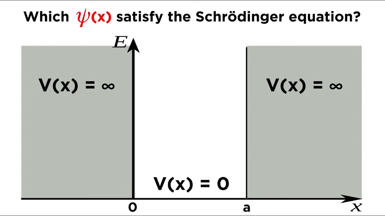
The Particle in One Dimensional Box is a fundamental quantum mechanical model where a particle (typically an electron) is confined to move only along one axis (x-axis). Unlike 3D or 2D boxes, movement is restricted to a single dimension. This model serves as an application of the Schrödinger equation to calculate electron energy levels. The box has infinite potential walls, meaning the particle cannot escape. Inside the box (0 < x < l), potential energy V = 0, while at boundaries (x = 0 and x = l), potential becomes infinite. The time-independent Schrödinger equation is d²ψ/dx² + (2mE/ħ²)ψ = 0, where (2mE/ħ²) = k². The general solution is ψ(x) = A sin(kx) + B cos(kx). Applying boundary conditions: at x = 0, ψ = 0 gives B = 0; at x = l, ψ = 0 gives sin(kl) = 0, requiring kl = nπ where n is a positive integer. Thus k = nπ/l, showing wave number quantization.
Click to watch →
Particle in a Box Part 1: Solving the Schrödinger Equation
426K
The particle in a box problem demonstrates how quantum mechanics naturally leads to quantized energy levels; by solving the time-independent Schrödinger equation for a particle confined in an infinite square well (where V(x) = 0 between x=0 and x=a, and V(x) = ∞ elsewhere), we find that the wavefunctions are ψₙ(x) = √(2/a) sin(nπx/a) with corresponding eigenenergies Eₙ = (n²π²ħ²)/(2ma²), where n is a positive integer, showing that only discrete energy states are allowed due to the boundary conditions ψ(0) = ψ(a) = 0.
Click to watch →

Quantum chemistry Lec -16| Schrodinger equation | CSIR-NET/JRF| GATE| IIT-JAM | DU
19.7K
This comprehensive lecture covers the fundamental principles of quantum mechanics as applied to chemistry. The instructor introduces the Schrödinger equation as an eigenvalue equation where applying an operator to a wave function returns the same wave function multiplied by a constant representing the system's energy. The Hamiltonian operator corresponds to total energy, and the time-independent Schrödinger equation (Ĥψ = Eψ) serves as the core mathematical framework. The instructor demonstrates mathematical manipulation of the equation, including differential operators and energy eigenvalue calculations. The particle in a box model is explored in detail, explaining the key difference between classical and quantum behavior: classical particles stop due to friction, while quantum particles move continuously without stopping. The model describes a particle confined to a one-dimensional box with potential energy zero inside and infinite outside. The instructor emphasizes that understanding these concepts is essential for solving quantum chemistry problems including vibrational motion, rotational motion, and hydrogen atom models.
Click to watch →

Examenspreekuur natuurkunde vwo met docenten Gerben en Ronit
73.6K
The particle in a box model describes quantum particles confined within a region with infinite potential walls, where the Schrödinger equation yields wave functions showing probability distributions that determine where particles are likely to be found; in the ground state, probability is zero at the edges and maximum in the center, while excited states show nodes where probability is zero, with energy levels given by E_n = (n²h²)/(8mL²) where n is the quantum number, h is Planck's constant, m is particle mass, and L is the box length.
Click to watch →

Motion of a Particle in 1dimensional rigid box | bsc 2nd yr Physics | Ankit sir | Physics Guru
29.8K
This comprehensive section covers the foundational concepts of quantum mechanics. The wave function (ψ) describes quantum states, with its square magnitude (|ψ|²) representing probability density. Complex numbers (z = x + iy) are essential for mathematical formulation. The particle in a one-dimensional box model demonstrates key quantum principles: a particle confined within length L with zero potential inside and infinite potential outside. This model illustrates wave-particle duality, energy quantization, and boundary conditions where ψ(0) = ψ(L) = 0. The time-independent Schrödinger equation (Ĥψ = Eψ) governs stationary states, with solutions yielding discrete energy levels and standing wave patterns.
Click to watch →
Deep Dive
Basic band theory of solids, including the concepts of valence bands, conduction bands, and the energy band gap in bulk semiconductors.

Basic Electronics:BANDGAP in material conductor semiconductor insulator Band theory of solid CB VB
587
Band theory of solids explains electronic properties through energy bands. The valence band is the highest energy band completely filled with electrons at absolute zero. The conduction band is above the valence band where electrons move freely. The band gap is the energy difference between these bands, determining whether a material is a conductor, semiconductor, or insulator. Semiconductors have a small band gap allowing electrons to jump with relatively small energy input.
Click to watch →

Band theory of solids | for Semiconductors, Conductors & Insulators |
4.7K
In solid-state physics, the valence band consists of filled energy levels containing electrons, while the conduction band consists of empty or partially filled energy levels above the valence band. The band gap is the energy difference between the top of the valence band and the bottom of the conduction band. Electrons must gain sufficient energy to cross this gap to participate in conduction. Materials are classified based on the size of this band gap: conductors have no band gap (bands overlap), semiconductors have small gaps, and insulators have large gaps.
Click to watch →

01 BASICS (PART 01) ENERGY BAND, CONDUCTION BAND, VALENCE BAND & BAND GAP
1.1K
In solid materials, discrete atomic energy levels merge to form continuous energy bands: the valence band (lower energy band containing bound electrons) and the conduction band (higher energy band containing free electrons that enable electrical conduction). The band gap is the energy difference between these two bands, which determines a material's electrical properties: conductors have zero band gap, semiconductors have a small band gap (e.g., silicon ~1.1 eV, germanium ~0.7 eV), and insulators have a large band gap.
Click to watch →

12th - Solid State (Lec - 3)
151
According to band theory, solids have energy bands: (1) Valence band - lower energy band containing bonding electrons, (2) Conduction band - higher energy band containing free electrons, (3) Band gap - energy difference between valence and conduction bands. The size of the band gap determines electrical properties: conductors have overlapping or very small band gaps, semiconductors have moderate band gaps (1-3 eV), and insulators have large band gaps (>3 eV). Molecular orbitals form from overlapping atomic orbitals, creating bonding orbitals (lower energy) and antibonding orbitals (higher energy). The number of energy bands depends on the number of atoms in the crystal.
Click to watch →

basic electronics theory | technical helper exam preparation |basic electronics theory and practice
1.2K
Semiconductors have two energy bands: valence band (bound electrons) and conduction band (free electrons). The band gap is the energy difference between these bands. Insulators have band gaps >7 eV (require huge energy for electron excitation), semiconductors have ~1 eV (moderate energy required), and conductors have ~0 eV (negligible gap). Electrons must gain sufficient energy to jump from valence to conduction band to conduct electricity. This band theory explains why different materials have different electrical properties.
Click to watch →
Deep Dive
The definition of nanomaterials and the physical significance of the nanoscale, particularly the dramatic increase in surface-to-volume ratio.
Nanomaterials Part I (Surface to Volume ratio, Types, Synthesis)
177
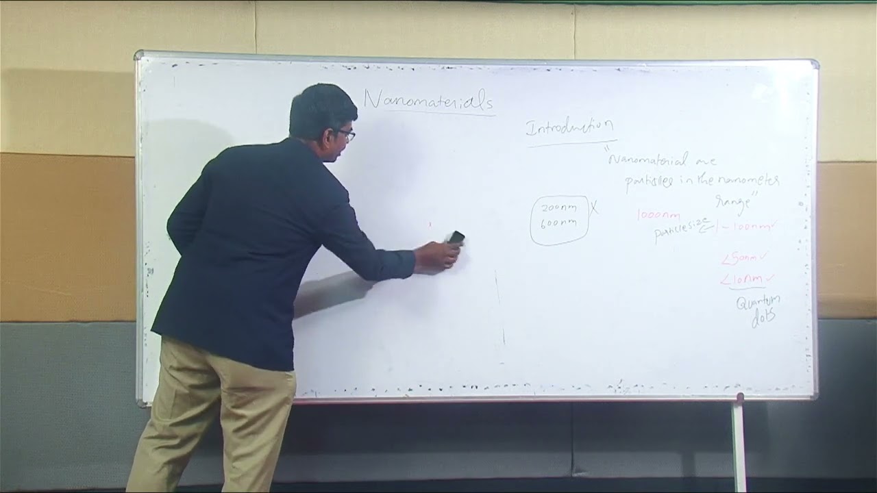
Nanomaterials are materials with particle sizes between 1 to 100 nanometers, universally accepted in nanotechnology. The surface to volume ratio is the key property making nanomaterials special. For spheres, the ratio is 3/R, inversely proportional to radius. As size decreases from 1 cm to 1 nm, the ratio increases from 3×10² to 3×10⁹. Surface atoms lack bonds in the outward direction, giving higher surface energy. The percentage of surface atoms increases dramatically: 50% for 3 nm particles, 20% for 10 nm particles, and only 5% for 30 nm particles. Nanomaterials are classified by dimensions outside the nano range: zero-dimensional (quantum dots, nanopowders), one-dimensional (nanotubes, nanowires), two-dimensional (thin films, nanosheets), and three-dimensional (bulk materials).
Click to watch →

Semiconductor Physics | Nano Technology One Shot in 15 Minutes | Pradeep Giri Sir
160
The surface-to-volume ratio is a critical concept in nanomaterials, referring to the amount of surface area compared to volume. At the nanoscale, particles become very tiny, dramatically increasing this ratio. This means a larger proportion of atoms are on the surface rather than in the interior. The surface area of a sphere is 4πr², while volume is (4/3)πr³. This high ratio leads to increased reactivity, better catalytic activity, special optical, electrical, and magnetic properties, and energy benefits such as faster charging in batteries and supercapacitors.
Click to watch →

AICTE - STTP On “Synthesis Characterization and its applications of Nanomaterials"
693
The surface-to-volume ratio for spherical particles follows the relationship S/V = 6/D, where D is the diameter. For a 100 nm particle, S/V ≈ 6 × 10⁷ m⁻¹, whereas for a 1 meter particle, S/V = 6 m⁻¹. This demonstrates why surface effects dominate at the nanoscale but are negligible in bulk materials. The definition of nanomaterials (dimensions below 100 nm) is directly tied to this dramatic increase in surface-to-volume ratio, which enables the unique properties that make nanotechnology so promising for applications ranging from electronics to medicine.
Click to watch →

Nanomaterials and their properties-session2-nptel-noc24-mm38
133
Nanomaterials are classified by how many dimensions are confined to nanoscale (less than 100 nm). Zero-dimensional nanomaterials have all three dimensions confined (e.g., gold nanoparticles, quantum dots). One-dimensional nanomaterials have two dimensions not confined (e.g., carbon nanotubes with diameter 10-50 nm but length >100 nm). Two-dimensional nanomaterials have one dimension not confined (e.g., thin films). Three-dimensional nanomaterials have no dimensions confined. As particle size decreases, surface area to volume ratio increases dramatically. For a cube, ratio is 6/a; for a sphere, ratio is 3/r. In bulk materials, most atoms are inside with fewer on surface. At nanoscale (around 1 nm), more than 99% of atoms are on surface because surface atoms become comparable to or exceed bulk atoms.
Click to watch →

NANOTECHNOLOGY | BY DR. NARSING RAO || MLRITM
106
Nanomaterials are classified by dimensionality: one-dimensional materials have one dimension at the nanoscale (nanowires, thin films); two-dimensional materials have two dimensions at the nanoscale (nanotubes); three-dimensional materials have all three dimensions at the nanoscale (quantum dots). When particle size decreases, surface-to-volume ratio increases dramatically—for spheres, the ratio is 3/r, meaning more atoms reside at surfaces rather than interiors. Dividing a 1m³ cube into eight smaller cubes doubles surface area from 6m² to 12m². This increased surface area enhances chemical reactivity, dissolution rates, and other properties, making nanoparticles more reactive than bulk materials.
Click to watch →
Deep Dive
The concept of excitons (electron-hole pairs) and the definition of the exciton Bohr radius in semiconductor materials.

Excitons and excitonic Bohr radius, energy levels, splitting
7.9K
Excitons are bound electron-hole pairs formed when photons with energy equal to or greater than the bandgap are absorbed by semiconductors, with their binding energy determined by Coulomb interactions and described by the exciton Bohr radius a_B* = (ε_R × m/μ) × a_B, where ε_R is the dielectric constant, m is the effective mass, μ is the reduced mass, and a_B is the hydrogenic Bohr radius; quantum confinement in nanoparticles (quantum dots) with sizes comparable to or smaller than the exciton Bohr radius causes the energy levels to become discrete rather than continuous, leading to size-dependent optical properties where smaller quantum dots exhibit blue-shifted emission (higher energy) and larger quantum dots show red-shifted emission (lower energy), with the total energy comprising band gap energy, confinement energy, and bound exciton energy.
Click to watch →

Quantum Confinement
137
The exciton Bohr radius represents the characteristic distance at which an electron and hole form a bound state through electrostatic attraction. This concept is analogous to the Bohr radius in atomic physics but applies to semiconductor materials. The exciton Bohr radius determines the spatial extent of excitons and influences their behavior in quantum-confined systems, affecting optical absorption and emission properties.
Click to watch →

Inorganic Phosphors I
419
The exciton Bohr radius is the average distance between an electron and hole in an exciton (bound electron-hole pair). When semiconductor crystal size becomes comparable to or smaller than this radius, quantum confinement effects dominate, transforming continuous energy levels into discrete states. This transition fundamentally changes the electronic and optical properties of the material.
Click to watch →

Fenómenos Colectivos en Materiales Cuánticos: Clase 22: Excitones
137
This section covers the exciton Bohr radius and its material dependence. The exciton Bohr radius is a_B = (4π ε_0 ε_r ħ^2) / (μ e^2), depending on reduced mass and dielectric constant. For typical semiconductors, the exciton Bohr radius is 10-100 nm, much larger than hydrogen's 0.53 Å. This large size means excitons are extended over many unit cells. The binding energy varies between materials: GaAs has about 4 meV, while materials with smaller band gaps have even smaller binding energies. This variation affects the temperature at which excitons can exist as bound states.
Click to watch →

ФНС. Лекция 11. Экситоны в наноструктурах - 1
471
The exciton Bohr radius in semiconductors is given by a formula similar to the hydrogen atom but with effective masses and dielectric constant. The exciton Bohr radius is typically much larger than the lattice constant (hundreds of angstroms), which is why excitons can be treated as particles with internal structure. The exciton energy is characterized by a binding energy that depends on the reduced mass of the electron-hole pair and the dielectric constant of the material.
Click to watch →
Prerequisite Knowledge
- Concept 01Fundamental concepts of quantum mechanics, specifically the 'particle in a box' model and the Schrödinger wave equation.
- Concept 02Basic band theory of solids, including the concepts of valence bands, conduction bands, and the energy band gap in bulk semiconductors.
- Concept 03The definition of nanomaterials and the physical significance of the nanoscale, particularly the dramatic increase in surface-to-volume ratio.
- Concept 04The concept of excitons (electron-hole pairs) and the definition of the exciton Bohr radius in semiconductor materials.
Subsequent Learning
- Step 01Practical applications of quantum dots (0D) in technologies such as QLED displays, solar cells, and biological imaging markers.
- Step 02Synthesis methods for nanomaterials (e.g., colloidal synthesis, chemical vapor deposition) and how to precisely control particle size to tune properties.
- Step 03Exploration of low-dimensional carbon allotropes, such as carbon nanotubes (1D) and graphene (2D), and their unique transport properties.
- Step 04Characterization techniques used to measure quantum confinement effects, such as UV-Vis absorption spectroscopy and photoluminescence spectroscopy.
Size Effects
Critical Size
Wave Match
Energy Levels
Band Tuning
Size Effects
1:03Playing Section
- 1
Nanomaterial properties change due to size reduction.
- 2
Quantum confinement becomes dominant at small scales.
- 3
Free electrons amplify size-dependent behavior.
The Breakdown of Effective Mass Approximation and Dominance of Surface Effects
While quantum confinement models (such as the Effective Mass Approximation) elegantly explain band gap tuning in moderately sized nanocrystals, they face severe limitations at extreme nanoscales, typically under 2 nanometers. At this limit, the assumption of a continuous bulk crystal potential breaks down, and the material's properties are better described by molecular orbital theory rather than bulk physics. Additionally, as size decreases, the surface-to-volume ratio skyrockets, meaning that electronic and optical properties are often dominated by surface states, ligand chemistry, and structural defects rather than pure quantum confinement. Critics argue that over-relying on simple confinement models overlooks these crucial chemical and structural realities, requiring a shift toward atomistic quantum chemical simulations.
Deep Dive
Practical applications of quantum dots (0D) in technologies such as QLED displays, solar cells, and biological imaging markers.

#sensors #quantumdots #nanotechnology Quantum Dots for sensing and switches applications
309
Quantum dots enable commercial applications including QLED television displays (improved color accuracy and brightness compared to OLED), solar cells (enhanced electron injection efficiency), and biomedical imaging. Research applications span sensing, imaging, transistors, and switches. Key advantages include straightforward fabrication, excellent stability from protective ligands, easy functionalization, and predictable optical properties. The tunable emission wavelength makes quantum dots highly versatile for developing sensors with tailored specifications for different analytical targets.
Click to watch →

LDC 2027 - TPL CHEMISTRY - ഇനി Easy! 😍 | Learn • Compete • Win 🏆| DEEPIKA MISS #ldc
14.6K
Quantum dots have several important applications: (1) Quantum LED TVs - provide better color accuracy and brightness, (2) Cancer treatment - help identify tumor cells with high precision, (3) Bio-imaging - allow detailed observation of cellular processes, (4) Solar panels - improve energy conversion efficiency, (5) LEDs - provide better light quality. These applications demonstrate the practical importance of quantum dot technology.
Click to watch →

Коллоидный синтез квантовых точек
5.1K
Quantum dots are characterized using TEM (size/shape), FTIR (surface stabilization), and XRD (phase composition/size). Applications include: (1) Laser media with tunable wavelength and high photostability, (2) QLEDs with tunable emission and thin-film formation, (3) Solar cells using nanocrystal photosensitizers with tunable band gaps, and (4) Biological fluorescent labels offering tunable wavelength, high photostability, and surface modification for selective targeting.
Click to watch →

Jueves de la Ciencia - Partículas confinadas en puntos cuánticos 04/12/2025
101
Quantum dots have diverse applications: (1) Solar cells - improving efficiency through intermediate band technology; (2) Displays - QLED televisions use quantum dots for vibrant colors; (3) Biomedical imaging - quantum dots can be injected into living organisms to track cells and organs; (4) LEDs - quantum dot LEDs provide efficient light emission; (5) Sensors - detecting various physical and chemical properties.
Click to watch →

Tapasztó Levente: Miért érdekes a nanovilág és mire képes a nanotechnológia?(Atomcsill, 2025.02.06.)
13.6K
Quantum dots have applications in displays (QLED), solar cells, biological imaging, and quantum computing. Their size-tunable optical properties make them superior to traditional fluorescent dyes for many applications.
Click to watch →
Deep Dive
Synthesis methods for nanomaterials (e.g., colloidal synthesis, chemical vapor deposition) and how to precisely control particle size to tune properties.
Synthesis of nanomaterials by Physical and Chemical Methods
269.3K
This lecture covers two main approaches to nanomaterial synthesis: physical methods (mechanical milling as a top-down process using ball mills to break bulk materials into nanoparticles, and laser ablation as a green method using laser light to vaporize targets and produce ultra-pure colloidal nanoparticles) and chemical methods (reduction method requiring metal salt, reducing agent, and capping agent, with nucleation and growth being the fundamental processes; the lecture also explains how particle size and shape can be controlled through parameters like nucleation rate, growth rate, and stabilizer concentration, with demonstrations of gold nanorod and silver nanoparticle synthesis experiments).
Click to watch →

Tecnología de partículas- Dra. Antonieta García Murillo y Dr. Felipe Carrillo, CIITEC
186
Two primary synthesis methods are used for nanomaterials: sol-gel and hydrothermal. Sol-gel involves hydrolysis and polymerization of metal precursors to form colloidal solutions (sol) that transform into gels, which can be processed into monoliths, coatings, fibers, powders, or aerogels through different drying methods. Hydrothermal synthesis uses an autoclave at 150-250°C to control particle morphology, size, and composition. These methods allow precise control over material properties including morphology, microstructure, purity, and homogeneity by adjusting parameters like temperature, pH, and reaction conditions.
Click to watch →
Synthesis and Characterization of Nanomaterials by Dr. Smita Chaturvedi,
657
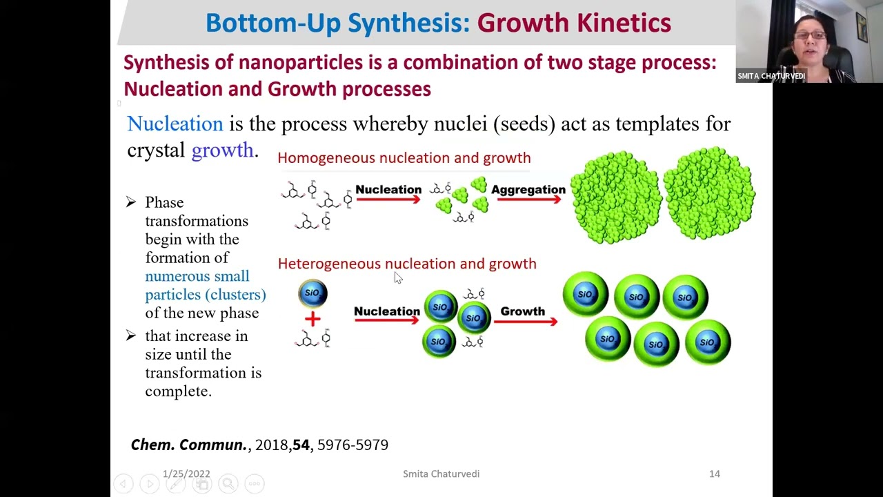
Nanomaterials exhibit unique properties due to their high surface-to-volume ratio and quantum confinement effects, which can be synthesized using either top-down approaches (reducing bulk materials) or bottom-up approaches (building from molecular precursors); bottom-up methods like physical vapor deposition (PVD) techniques (inert gas condensation, evaporation, plasma arcing, laser ablation, sputtering, and chemical vapor deposition) and liquid-phase methods (colloidal synthesis, wet chemical methods, sol-gel process, microemulsion, and spray pyrolysis) allow control over particle size, shape, and structure, which ultimately determines the material's physical, optical, and electrical properties.
Click to watch →
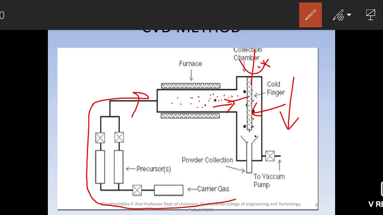
Synthesis of nanomaterials- CVD method-Prof.Shwethambika.P.
5.9K
The Chemical Vapor Deposition (CVD) method is a bottom-up approach for synthesizing nanomaterials where metallo-organic compounds serve as precursors and are transported by a carrier gas (typically argon) into a heated furnace, where thermal decomposition produces nanoparticles that condense and deposit onto a liquid nitrogen-cooled rotating substrate (coldfinger), allowing precise control over particle size, shape, and composition through adjustment of temperature, precursor concentration, and flow rates.
Click to watch →

NANO MATERIALS AND APPLICATIONS: Colloidal synthesis
2.7K
Colloidal synthesis is a wet chemical precipitation technique for producing nanomaterials by mixing solutions of different ions under controlled temperature and pressure to form insoluble precipitates; this method is simple, allows precise control over particle size and shape, and is widely used for synthesizing metals, metal oxides, and organic compounds for applications in pharmaceuticals and medicine, though it faces limitations including stability issues and the need for stabilizers.
Click to watch →
Deep Dive
Exploration of low-dimensional carbon allotropes, such as carbon nanotubes (1D) and graphene (2D), and their unique transport properties.

Como o GRAFENO mudará o mundo – Tudo sobre o grafeno
4M
Carbon's ability to form different geometric structures creates diverse allotropes with distinct properties. Diamond features a tetrahedral 3D structure with four covalent bonds per carbon atom, making it transparent, extremely hard, and an electrical insulator. Graphite consists of hexagonal carbon sheets held by weak van der Waals forces, creating a soft, conductive material. Graphene represents a single hexagonal sheet of carbon atoms, one atom thick. Carbon nanotubes form cylindrical structures from rolled graphene sheets, while fullerenes create spherical buckyball structures. These different arrangements produce materials ranging from the hardest natural substance (diamond) to the softest (graphite), demonstrating how atomic geometry determines macroscopic properties.
Click to watch →

Pt-3 कार्बन की सर्वतोमुखी प्रकृति व अपररूप | Versatile Nature of Carbon & Allotropes | Nano-Tech
187K
Graphene, discovered in 2004, is the thinnest and strongest material known, consisting of a single carbon atom layer in hexagonal arrangement. It is transparent, flexible, and has exceptional electrical conductivity. Graphene can be produced by mechanically exfoliating graphite with adhesive tape. Carbon nanotubes are cylindrical structures made of rolled graphene sheets, approximately 100 times stronger than steel while being much lighter. These materials have applications in aerospace, automotive, electronics, and energy storage. Graphene's exceptional properties make it promising for future technologies including advanced composites, flexible electronics, and energy storage systems.
Click to watch →

HSC || Organic Chemistry || Class-01 || এইচএসসি || জৈব রসায়ন || ক্লাস-০১
404.3K
Carbon allotropes include: (1) Diamond (sp3 hybridization, all single bonds), (2) Graphite (sp2 hybridization, all single bonds), (3) Fullerenes (sp2 hybridization, with double bonds), (4) Carbon nanotubes, and (5) Nanotubes. The instructor emphasizes that understanding carbon allotropes is essential for understanding the diverse properties of carbon.
Click to watch →

The New “Impossible” Engine
2.6K
Carbon nanotubes are 4-5 times lighter than copper, cheaper, and less attractive to thieves, but must conduct as well as copper to be viable. Carbon allotropes like graphite and diamond have vastly different properties due to their energy band structures. Graphene (single-layer graphite) conducts electricity very fast in 2D, but wires are 3D structures. Carbon nanotubes are rolled graphene sheets that maintain 2D conductivity in 3D form. Production challenges include impurities at the atomic level, requiring sophisticated methods like wet spinning (drawing fibers through acid baths and twisting like yarn) and the LAST process (Lyotropic Liquid Crystal Assisted Surface Texturing) which improved conductivity by 30%.
Click to watch →

The Materials of the Future: Interesting Allotropes of Carbon
17.9K
Carbon allotropes are different structural forms of carbon atoms that exhibit dramatically different properties; for example, carbon nanotubes are cylindrical structures made of carbon rings that are as strong as diamond but incredibly lightweight, while graphene is a single layer of carbon atoms arranged in a hexagonal lattice that conducts heat and electricity extremely efficiently and is approximately 100 times stronger than steel.
Click to watch →
Deep Dive
Characterization techniques used to measure quantum confinement effects, such as UV-Vis absorption spectroscopy and photoluminescence spectroscopy.
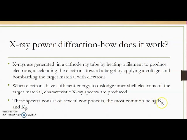
X-ray diffraction analysis,PL and UV spectroscopy
318
This lecture covers three characterization techniques for nanostructure materials. X-ray diffraction analysis provides structural information including grain size, micro distortion, texture, and lattice parameters. Nano crystalline materials exhibit different properties than bulk materials. The technique is based on constructive interference of monochromatic X-rays with crystalline samples, governed by Bragg's law (λ = 2D sinβ). X-ray systems generate characteristic spectra (K-alpha, K-beta) from target materials. UV spectroscopy measures absorption/reflectance in UV-visible regions for material identification, with absorption affecting perceived color. Atoms and molecules undergo electronic transitions: absorption measures ground state to excited state transitions, while fluorescence measures excited state to ground state. Molecules with bonding/non-bonding electrons absorb UV/visible light to excite electrons to antibonding orbitals (σ to σ*, n to σ*, π to π*, n to π*). Photoluminescence is a non-destructive optical method where light absorption imparts energy, and excess energy is dissipated through luminescence (spontaneous emission from excited to ground state). The intensity and spectral content of photoluminescence provide direct measures of material properties.
Click to watch →
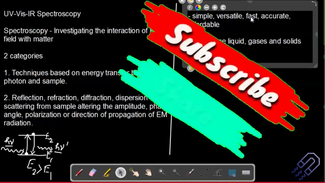
Waves Physics Lectures | Characterization Techniques | UV- Vis spectroscopy
198
UV-Vis spectroscopy is a characterization technique that investigates the interaction of electromagnetic radiation with matter by measuring how materials absorb light in the ultraviolet (300-400 nm) and visible (400-765 nm) regions; the technique works by promoting electrons from lower to higher energy states when photon energy matches the energy gap between molecular orbitals, with four main electronic transitions (σ→σ*, n→σ*, π→π*, and n→π*) occurring at different wavelengths, and the instrumentation typically includes a light source, monochromator, sample holder, and detector, with common designs being single-beam, double-beam, and simultaneous spectrometers.
Click to watch →
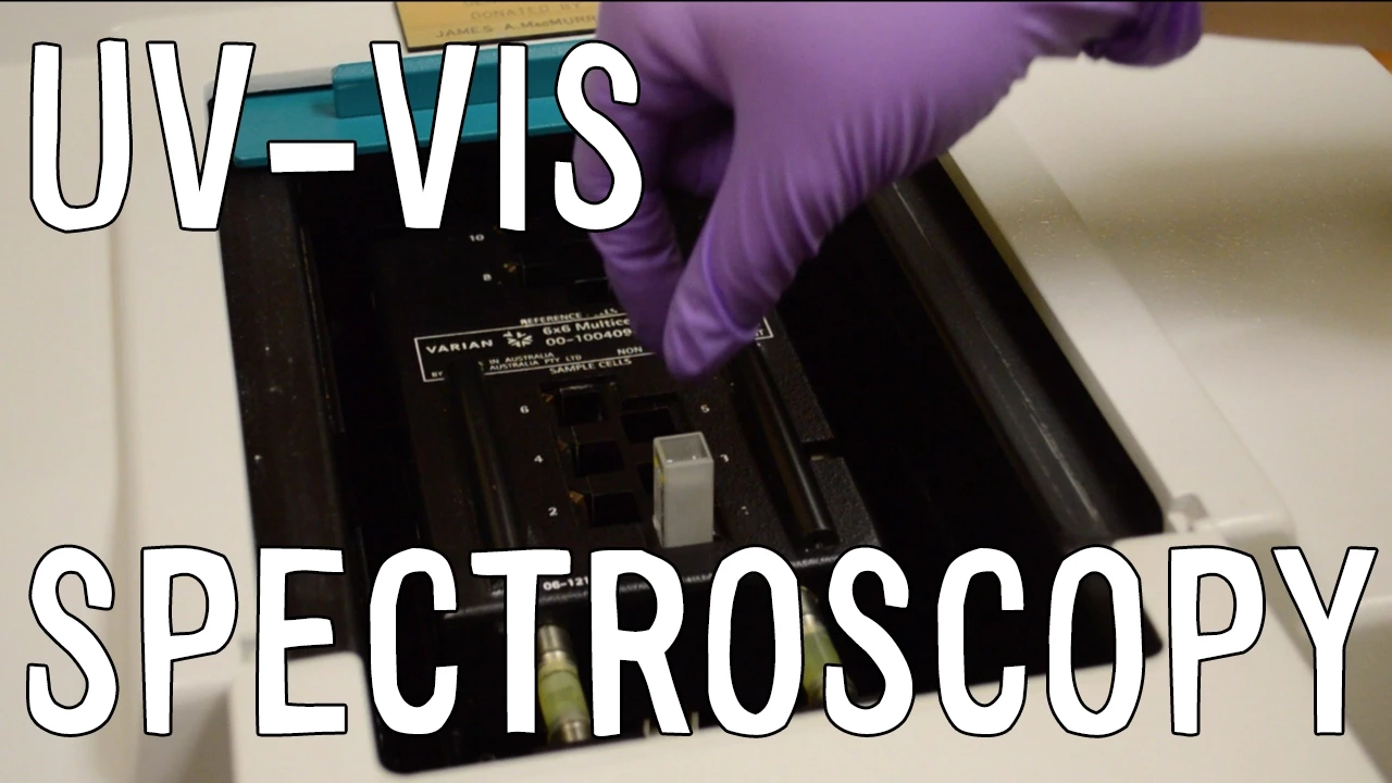
How to Use a UV-Vis Spectrometer
241.1K
A UV-Vis spectrometer measures the absorption of light by a sample to characterize coordination compounds through electron transitions between d-orbitals; proper operation requires selecting the appropriate cuvette material (plastic for aqueous solutions, glass for visible range, quartz for UV range), preparing homogeneous samples by dissolving solids or diluting concentrated liquids, performing baseline correction with solvent blanks, and analyzing the resulting absorption spectrum to determine peak wavelengths and absorbance values.
Click to watch →

UV-Vis Tutorial | Part 1: Intro to Measuring Nanoparticles
100.3K
UV-Vis spectroscopy measures the absorbance of nanoparticle solutions across ultraviolet and visible light wavelengths to determine material properties, nanoparticle size, and sample quality; the technique requires blanking the instrument with the dispersing solvent to account for background absorption, and optimal measurements require diluting concentrated samples to achieve an absorbance of approximately 0.8-1.1 OD for clear, defined spectral peaks.
Click to watch →
Chem 232 050824
130
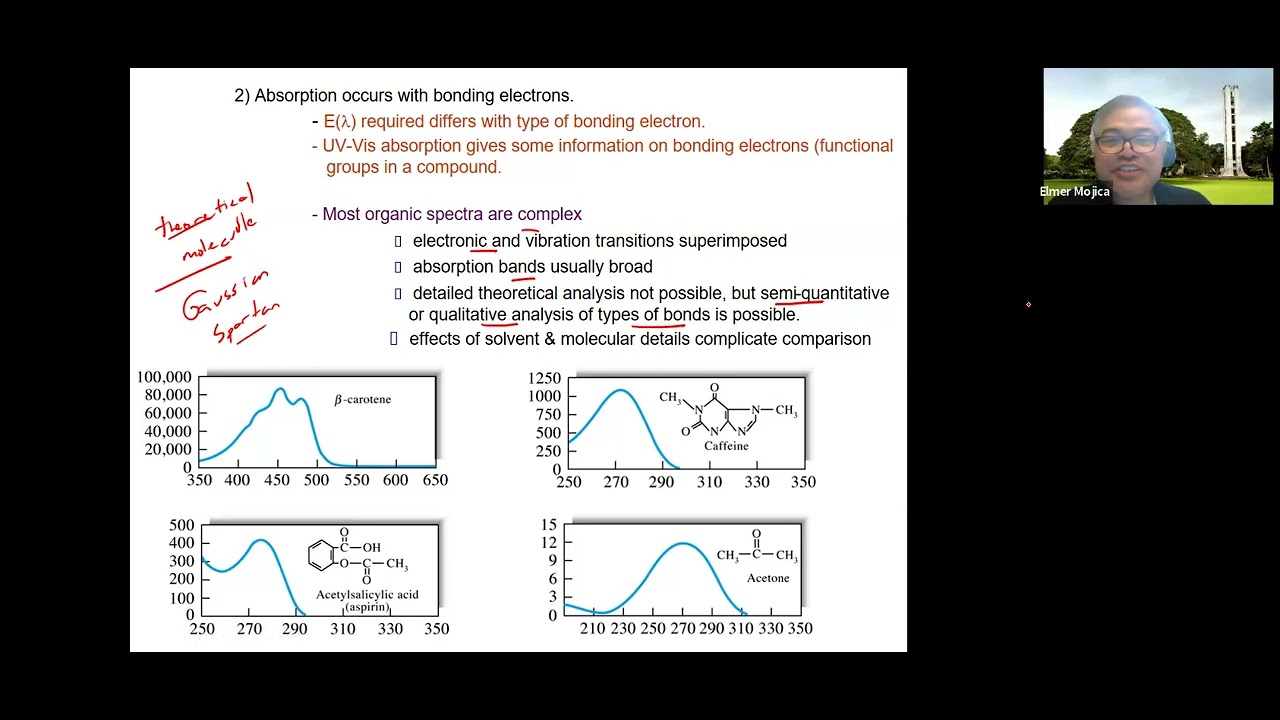
UV-Vis absorption spectroscopy is the most widely used quantitative analytical technique in chemical, environmental, forensics, and clinical laboratories. It measures absorption of ultraviolet and visible light for identification and determination of inorganic and organic substances. Key characteristics include wide applicability to organic and inorganic systems, detection from 10^-4 to 10^-7 M, moderate to high selectivity, and relative uncertainties of 1-3%. The technique involves electronic excitation where photons are absorbed to produce excited states (M*) with lifetimes of 10^-8 to 10^-9 seconds. Relaxation occurs through fluorescence, phosphorescence, or photochemical decomposition. All organic compounds absorb electromagnetic radiation due to valence electrons that can be excited to higher energy levels.
Click to watch →
Size Effects
Critical Size
Wave Match
Energy Levels
Band Tuning
Size Effects
1:03- 1
Nanomaterial properties change due to size reduction.
- 2
Quantum confinement becomes dominant at small scales.
- 3
Free electrons amplify size-dependent behavior.
The Breakdown of Effective Mass Approximation and Dominance of Surface Effects
While quantum confinement models (such as the Effective Mass Approximation) elegantly explain band gap tuning in moderately sized nanocrystals, they face severe limitations at extreme nanoscales, typically under 2 nanometers. At this limit, the assumption of a continuous bulk crystal potential breaks down, and the material's properties are better described by molecular orbital theory rather than bulk physics. Additionally, as size decreases, the surface-to-volume ratio skyrockets, meaning that electronic and optical properties are often dominated by surface states, ligand chemistry, and structural defects rather than pure quantum confinement. Critics argue that over-relying on simple confinement models overlooks these crucial chemical and structural realities, requiring a shift toward atomistic quantum chemical simulations.
Fundamental concepts of quantum mechanics, specifically the 'particle in a box' model and the Schrödinger wave equation.
Basic band theory of solids, including the concepts of valence bands, conduction bands, and the energy band gap in bulk semiconductors.
The definition of nanomaterials and the physical significance of the nanoscale, particularly the dramatic increase in surface-to-volume ratio.
The concept of excitons (electron-hole pairs) and the definition of the exciton Bohr radius in semiconductor materials.
Practical applications of quantum dots (0D) in technologies such as QLED displays, solar cells, and biological imaging markers.
Synthesis methods for nanomaterials (e.g., colloidal synthesis, chemical vapor deposition) and how to precisely control particle size to tune properties.
Exploration of low-dimensional carbon allotropes, such as carbon nanotubes (1D) and graphene (2D), and their unique transport properties.
Characterization techniques used to measure quantum confinement effects, such as UV-Vis absorption spectroscopy and photoluminescence spectroscopy.
48K views672likes13:25@TheUltimatePhysicsChannelOriginal Release: 2019-12-14
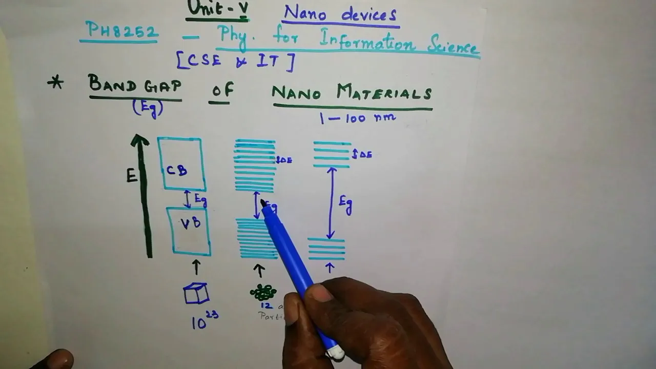
because free electrons in any system therefore any size effect is going to play the properties of the what is the difference between a million and again and why quantum confinement is effective one nanomaterials reduce size the bulk solid now this is not several greats but one or two what stage they start dominating there are two ways one can put this up we can talk about for example they probably take them when the size of the drain is a size of the grain that is a D and the size of the grain is comfortable so they probably wavelength of the moving electron then what X starts to show up so why is this happening why it affects the energy levels in the first place is very interesting we know in quantum mechanics one of the first problems that we do is what is called particle in a one dimensional box but also of the neck infection material drastically the emission absorption properties are going to vary to the emission and absorption properties of many cigarettes by tuning the band gap and the pan can be tuned in the Nano size manipulation size reduction thereby leading to very interesting properties because the electron is not that small even going to get drastically affect that because of the size affection so see some of the fundamental ethics that one sees Verisign sriracha nanomaterials this is a very very important chapter
Up Next
6:24
Band Gap of Nanomaterials Explained | Physics Lecture
@physicsfreak3567
20.2K views•2020-04-08
73:35
Deriving Maxwell's Equations in Geometric Algebra (QED Prereqs) 11
@XylyXylyX
2.6K views•2024-09-08

32:32
NMR Spin Physics I: Zeeman Effect, Resonance Condition & Larmor Frequency
@nptel-indianinstituteofsci8064
2.3K views•2024-01-17

33:44
The Blue LED: A Decade-Long Scientific Challenge Explained
@veritasium
46.5M views•2024-02-08
Related Study Plans & Knowledge Roadmaps
Structured learning paths in Physics
physics
Medical Physics: Imaging, MRI & Radiotherapy
01Foundations of Radiation and Matter Interaction
02X-Ray Imaging and Computed Tomography (CT)
03Magnetic Resonance Imaging (MRI) Physics
+ 3 more learning modules
15h6 modules
Explore Roadmap
physics
Nuclear Physics (Decay, Fission & Reactors)
01Atomic Structure and the Binding Force
02Radioactive Decay and Half-Life
03Nuclear Fission Mechanics and Chain Reactions
+ 2 more learning modules
12h5 modules
Explore Roadmap
physics
Soft Matter (Polymers, Colloids & Rheology)
01Foundations of Soft Matter & Thermal Forces
02Polymer Physics and Macromolecules
03Colloids, Surfactants, and Self-Assembly
+ 2 more learning modules
38h5 modules
Explore Roadmap
physics
Analytical Mechanics: Lagrangian & Hamiltonian
01Mathematical Foundations: Calculus of Variations
02From Newtonian Mechanics to Constraint Dynamics
03The Principle of Least Action & Lagrangian Mechanics
+ 3 more learning modules
28h6 modules
Explore Roadmap