












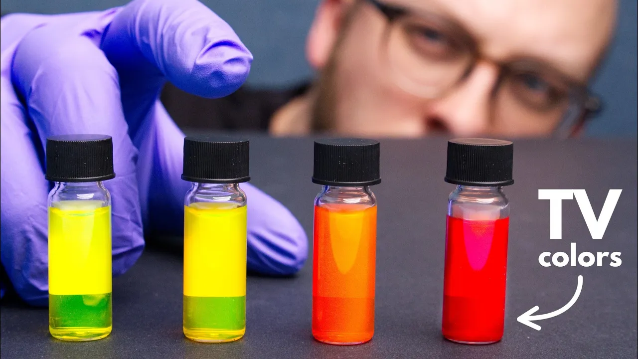








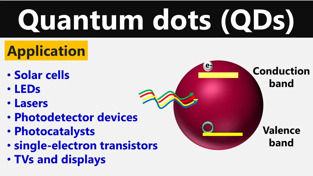



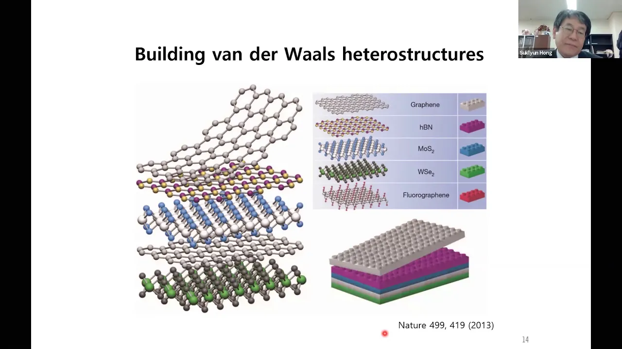

When bulk materials are reduced to nanoscale dimensions (1-100 nm), the band gap—the energy difference between the valence and conduction bands—increases due to quantum confinement effects, which fundamentally alters the electrical and optical properties of semiconductors for optoelectronic applications.
Band Gap of Nanomaterials Explained | Physics Lecture
Added:Basic band theory of solids, including the concepts of valence bands, conduction bands, and Fermi levels.
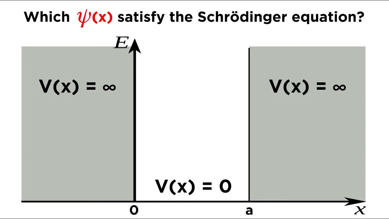
Fundamental quantum mechanics principles, particularly the 'particle in a box' model and the Schrödinger equation.
Standard semiconductor physics, including the behavior of charge carriers (electrons and holes).
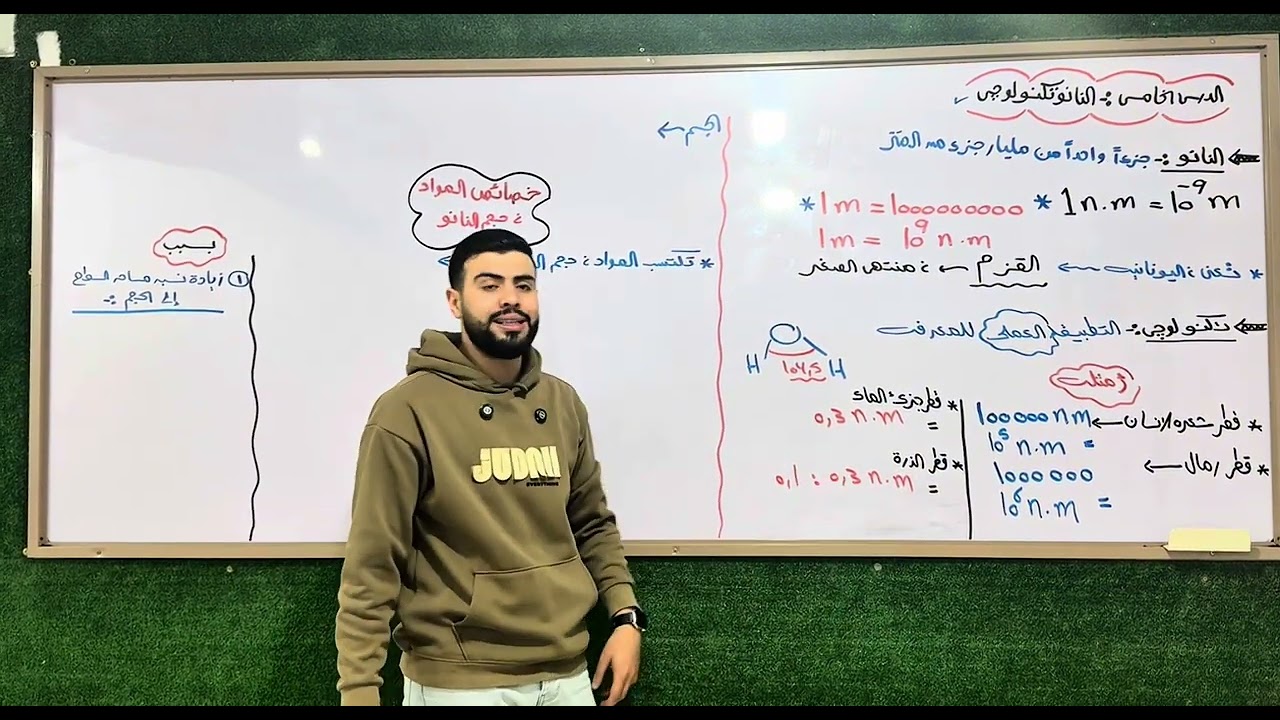
An introductory understanding of the nanoscale and how physical properties change at the dimension of 1-100 nanometers.
The physics and engineering of Quantum Dots (0D nanomaterials) and their use in QLED displays and biological imaging.
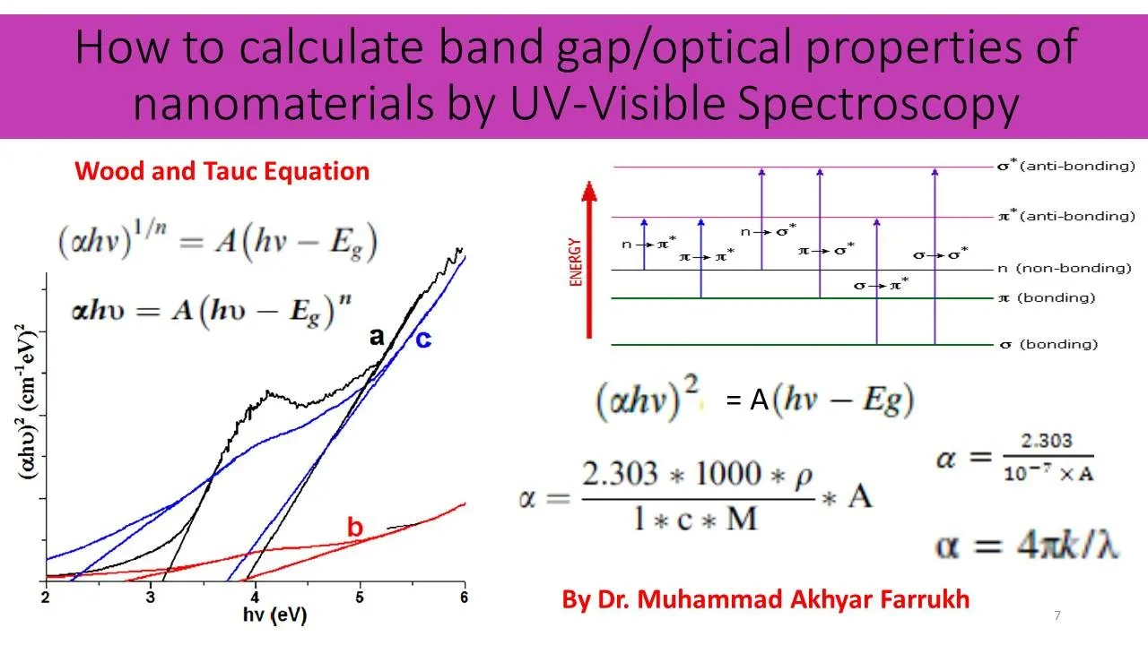
Experimental characterization techniques for nanomaterials, such as UV-Vis Spectroscopy to measure band gap shifts.
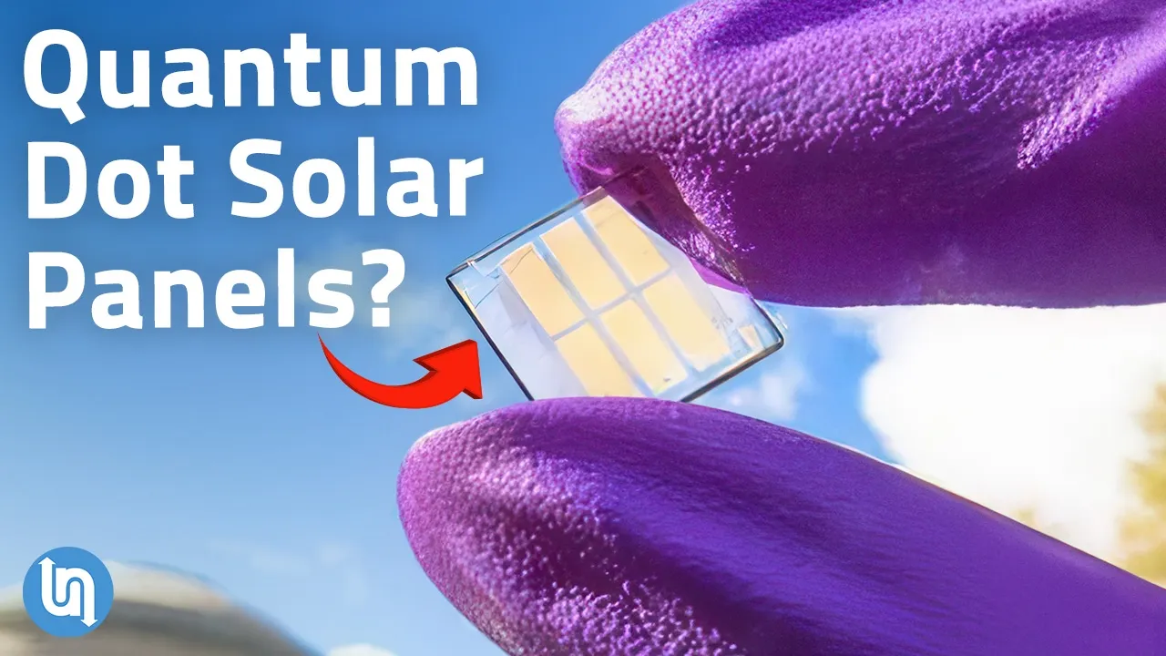
Applications of tunable band gaps in next-generation optoelectronic devices, including quantum dot solar cells and photodetectors.
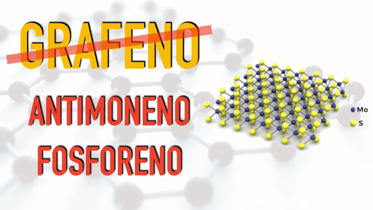
The study of 2D materials (like graphene and transition metal dichalcogenides) and their unique electronic structures.
20.2K views460likes6:24Original Release: 2020-04-08
hi everyone this is dr. Anthony assistant professor of physics our MD Engineering College today's topic is bandgap of nanomaterials in the unit 5 nano devices the subject name is physics for information science and the subject code is pH 8 - 5 - what are nanomaterials nanomaterials are small sized materials ranging between 1 to 100 nanometer what is a bandgap bandgap is the energy gap or energy separation or even energy difference between the valence band and the conduction band how energy bands are formed for simplicity and better understanding let us consider an isolated silicon atom the atomic number of silicon is 14 the 14 electrons are distributed in the case L M since as 2 8 & 4 respectively the electronic configuration can be written as 1s2 2s2 2p6 3s2 and 3p - an isolated atom possesses discrete energies of different electrons if we draw that for a single silicon atom 1s2 2s2 2p6 three years two and three p2 this is for one silicon atom consider I have one more silicon atom here and the discrete energy levels of that silicon atom has been thrown when these two atoms are brought closer together what will happen they form a combined system and the energies will not be in the same level but it will change they form a closely spaced two energy levels such as oneness of one silicon atom and the oneness of another silicon atom will be formed similarly for - yes - and for 2p6 3s2 and 3p to consider a bulk silicon material the three-dimensional solid one centimeter cube volume of a three dimensional solid material consists of 10 power 23 atoms then 10 power 23 closely spaced energy levels are formed instead they merge together and an energy band is formed likewise thus a bulk material has thick energy bands due to merging of adjacent energy levels of these large volume of atoms in between the energy bands there are ranges of energy which are entirely impossible known as forbidden energy this is the region forbidden for the electrons what will happen when the size of the bulk material is reduced during the reduction process based on the number of atoms present in the given volume the number of overlapping of energy levels decreases this will cause an increase in the energy gap between conduction band and the valence band here dele denotes the spacing between the sub shells let us consider a particle in which there are 12 atoms in the reduced volume there will be discrete energy levels in the particle and the band gaps become whiten now when the particle is further reduced so that the particle has only four atoms in it the removal of atoms adjust the boundaries of the band gap and the sub shells split and also we can see that the spacing between the sub shells increases thus in large volume bulk material a small band gap is present and when its volume gets reduced its band gap increases the electron is excited or D excited across the band gap the energy absorbed during excitation and released during excitation will be equal to the band gap energy of the material due to quantum confinement effect the electrons and holes are confined in semiconductors in the nano scale especially the energy difference between the filled state and the empty states in Risa's or widen the bandgap of semiconductor band gaps play a fundamental role in the electrical and optical properties of semiconductor materials in opto electronic devices this larger band gap drastically changes the optical and electronic properties of semiconductors at nanoscale so far we have completed about bandgap of nanomaterials let us all meet in the next video lecture thank you
Up Next

10:20
Create Graphene & Carbon Nanotubes in Atomistix ToolKit
@NoobResearcher
304 views•2024-02-26
73:35
Deriving Maxwell's Equations in Geometric Algebra (QED Prereqs) 11
@XylyXylyX
2.6K views•2024-09-08

32:32
NMR Spin Physics I: Zeeman Effect, Resonance Condition & Larmor Frequency
@nptel-indianinstituteofsci8064
2.3K views•2024-01-17

33:44
The Blue LED: A Decade-Long Scientific Challenge Explained
@veritasium
46.5M views•2024-02-08
Related Study Plans & Knowledge Roadmaps
Structured learning paths in Physics
physics
Medical Physics: Imaging, MRI & Radiotherapy
01Foundations of Radiation and Matter Interaction
02X-Ray Imaging and Computed Tomography (CT)
03Magnetic Resonance Imaging (MRI) Physics
+ 3 more learning modules
15h6 modules
Explore Roadmap
physics
Nuclear Physics (Decay, Fission & Reactors)
01Atomic Structure and the Binding Force
02Radioactive Decay and Half-Life
03Nuclear Fission Mechanics and Chain Reactions
+ 2 more learning modules
12h5 modules
Explore Roadmap
physics
Soft Matter (Polymers, Colloids & Rheology)
01Foundations of Soft Matter & Thermal Forces
02Polymer Physics and Macromolecules
03Colloids, Surfactants, and Self-Assembly
+ 2 more learning modules
38h5 modules
Explore Roadmap
physics
Analytical Mechanics: Lagrangian & Hamiltonian
01Mathematical Foundations: Calculus of Variations
02From Newtonian Mechanics to Constraint Dynamics
03The Principle of Least Action & Lagrangian Mechanics
+ 3 more learning modules
28h6 modules
Explore Roadmap