Atomic Force Microscopy (AFM) is a scanning probe technique that creates three-dimensional images of material surfaces by measuring the deflection of a sharp tip attached to a flexible cantilever as it scans across the surface; the tip experiences attractive forces when far from the surface and repulsive forces when close, with the cantilever bending according to Hooke's law, and this deflection is detected by reflecting a laser beam off the cantilever onto a photodetector, enabling resolution down to 0.1 nm vertically and 30 nm laterally, with three primary imaging modes (contact, non-contact, and tapping) suited for different sample types.
Atomic Force Microscopy (AFM) Explained: How It Works and Key Modes
Added:Deep Dive
Basic concepts of intermolecular forces, particularly Van der Waals forces and the Lennard-Jones potential.

Complete Class 11th INORGANIC CHEMISTRY: Make Your Basics Super Strong || Lakshya JEE 2026🔥
390.2K
Van der Waals forces are weak intermolecular forces that include: (1) Dipole-dipole forces - between polar molecules; (2) Dipole-induced dipole forces - between polar and non-polar molecules; (3) London dispersion forces (induced dipole-induced dipole forces) - between non-polar molecules. These forces are directly proportional to molecular surface area. Larger molecules with greater surface area have stronger Van der Waals forces. The strength order is: dipole-dipole > dipole-induced dipole > London dispersion forces.
Click to watch →

রসায়নের ২য় অধ্যায় || একটি ক্লাসে সম্পূর্ণ কম্পিলিট || ১০০% কমন || SSC Chemistry Chapter 2
188.4K
Van der Waals forces (ভ্যান্ডারওয়ালস আকর্ষণ বল) are intermolecular attractive forces. The strength of these forces is inversely related to intermolecular distance - greater distance means weaker forces. Gases have the weakest Van der Waals forces due to large intermolecular distances. This explains why gases are most compressible.
Click to watch →
![অধ্যায় ৩: মৌলের পর্যায়বৃত্ত ধর্ম ও রাসায়নিক বন্ধন: পোলারন এবং ভ্যান্ডার ওয়ালস বল [HSC]](https://i.ytimg.com/vi/HB3BXjsf9UM/hqdefault.jpg?v=63b504e2)
অধ্যায় ৩: মৌলের পর্যায়বৃত্ত ধর্ম ও রাসায়নিক বন্ধন: পোলারন এবং ভ্যান্ডার ওয়ালস বল [HSC]
110K
Chemical forces are categorized as intranuclear, intramolecular, interatomic, and intermolecular. Intermolecular forces include ionic bonding, Van der Waals forces, dipole-dipole attraction, and hydrogen bonding. Van der Waals forces are the weakest intermolecular forces (1-10 kJ/mol) occurring in pure covalent compounds. They are most visible in gaseous molecules like H2, O2, and Cl2. When molecules are within 5mm, electrons become asymmetrically distributed, creating temporary partial charges that attract neighboring molecules.
Click to watch →

FORÇAS INTERMOLECULARES (VAN DER WALLS) | Resumo de Química para o Enem
204.9K
Van der Waals forces are intermolecular attractions that determine physical properties like melting and boiling points; they include three types in order of increasing strength: induced dipole forces (weakest, occurring in nonpolar molecules through momentary charge fluctuations), dipole-dipole forces (stronger, occurring between polar molecules with permanent positive and negative poles), and hydrogen bonding (strongest, occurring when hydrogen is bonded to fluorine, oxygen, or nitrogen, creating a network structure); substances with stronger intermolecular forces have higher melting and boiling points, and solubility follows the principle that 'like dissolves like' based on these interaction types.
Click to watch →

Vander Waals Forces!Day-1!B.Sc 1st Semester Chemistry!Be DKDian
89.1K
Van der Waals forces are weak attractive forces that exist between molecules, responsible for holding molecules together in substances and determining their physical states (solid, liquid, gas). These forces are distinct from covalent bonds (which hold atoms together within molecules) and are responsible for phenomena like real gas deviation from ideal gas behavior and gas liquefaction.
Click to watch →
Deep Dive
Hooke's Law and the fundamental mechanics of spring constants and cantilever deflection.

Hooke's Law explained | झुन्नीलाल की चक्की का Spring वाला तराजू
187.8K
Hooke's Law states that the restoring force exerted by a spring is directly proportional to its displacement from equilibrium (F = -kx), where the spring constant k determines how much the spring stretches or compresses under a given force; when a spring is cut in half, its spring constant doubles because the number of coils is halved, making it stiffer and causing it to show less deformation for the same applied force.
Click to watch →

Cantilever for B.Sc. First year || Cantilever Loaded at free end for B.Sc. 2nd year || L-10
63.2K
A cantilever is a beam of uniform cross-sectional area fixed horizontally at one end and loaded at the other end. For a light cantilever (neglecting beam weight) with a point load W at the free end, the deflection at the free end is given by δ = (W L³)/(3 Y I), where L is the length, Y is Young's modulus, and I is the moment of inertia. For a rectangular cross-section (breadth B, depth D), I = (B D³)/12, so δ = (4 W L³)/(Y B D³). For a circular cross-section (radius R), I = (π R⁴)/4, so δ = (4 W L³)/(3 π Y R⁴).
Click to watch →

GIC & UPPGT PHYSICS || Mechanics-25 || Elasticity and Elastic Constants by Anup kushwaha
19K
When a beam is supported at both ends and loaded in the middle, the upper surface experiences tension while the lower surface experiences compression. The neutral axis experiences neither. For a cantilever beam fixed at one end and loaded at the free end, the depression is: Δ = (Wl³)/(3EI). For a cantilever with load at the center: Δ = (Wl³)/(8EI). The moment of inertia (I) for rectangular cross-section is (bd³)/12, and for circular is (πr⁴)/4. Beam depression is proportional to load, cube of length, and inversely proportional to Young's modulus and moment of inertia.
Click to watch →

Beam Deflection Using Double Integration Method
152.4K
Beam deflection is the deformation of structural members from their original position under load. Key influencing factors include load magnitude/type, span length, material properties (modulus of elasticity E), cross-sectional shape (moment of inertia I), and beam type. Standard formulas for common configurations are: simply supported with uniform load: Δ_max = 5WL⁴/(384EI); simply supported with concentrated load at midspan: Δ_max = PL³/(48EI); cantilever with concentrated load at free end: Δ_max = PL³/(3EI). The mathematical foundation uses the governing differential equation EI(d²y/dx²) = M(x), where integration yields slope and deflection equations with constants determined by boundary conditions: simply supported beams have zero deflection at both ends; cantilever beams have zero deflection and zero slope at the fixed end.
Click to watch →
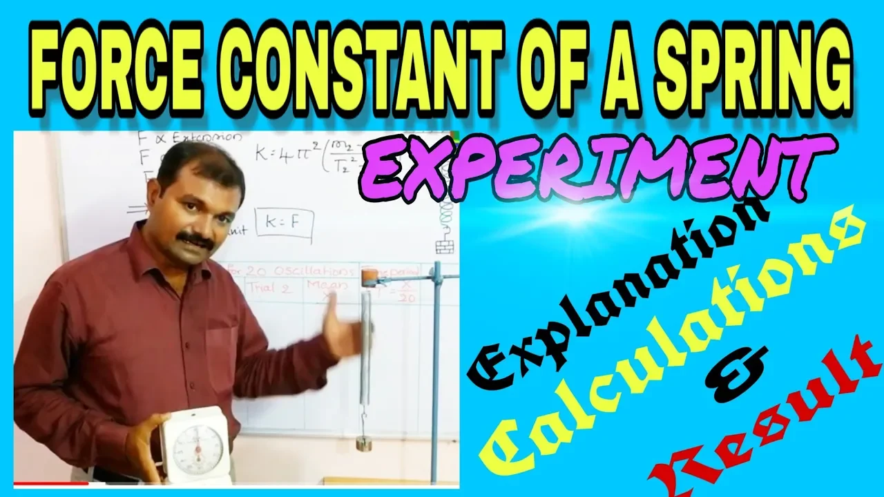
Force constant of a spring
122.8K
The force constant, commonly referred to as the spring constant in physics, is defined as the force per unit displacement, expressed by the formula k = F/X, where F is the applied force and X is the displacement. Its dimensional formula is M¹T⁻², derived from the dimensions of force (M¹L¹T⁻²) divided by displacement (L¹). The SI unit of the force constant is newtons per meter (Nm⁻¹). This concept is central to Hooke’s law, which states that the force required to extend or compress a spring is directly proportional to the distance of deformation, provided the deformation is small relative to the spring’s total possible deformation. Hooke’s law applies not only to springs but also to other elastic systems such as wind-induced deformation of tall buildings, plucked guitar strings, and inflated party balloons. Materials obeying this linear relationship are termed linear-elastic or Hookean. The law enables the derivation of material-specific relationships between strain and stress. For instance, a homogeneous rod with uniform cross-section behaves like a spring when stretched, with its stiffness k directly proportional to its cross-sectional area and inversely proportional to its length.
Click to watch →
Deep Dive
The piezoelectric effect and how it is used for precise nanoscale positioning and movement.
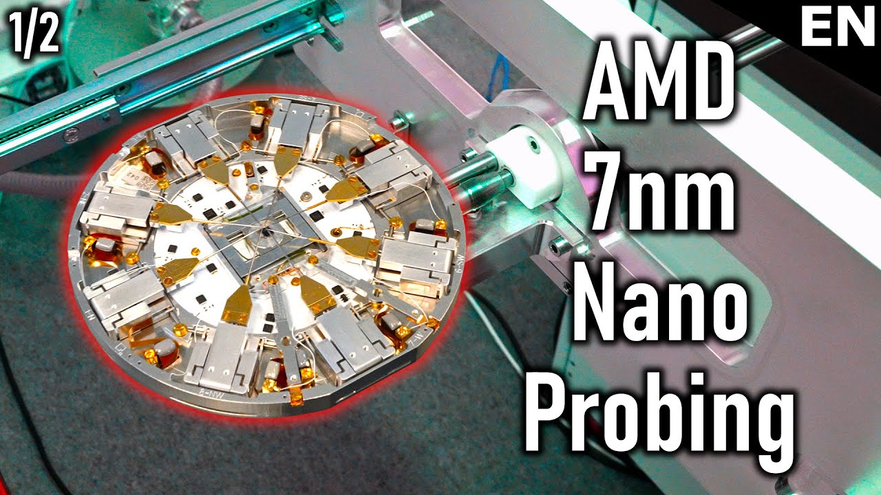
Unreal Precision - Analyzing a Single TSMC 7nm Transistor. Visiting Kleindiek Part 1/2
211.4K
Piezoelectric elements form the foundation of Kleindig's nanomanipulation technology. These elements generate mechanical movement when voltage is applied, or produce electrical signals when mechanically stressed. The principle is demonstrated in electric lighters, where pressing a button applies pressure to a crystal, generating voltage that creates a spark. Conversely, applying voltage to the crystal can change its length or size on a nanometer scale with extreme precision.
Click to watch →

Record player cartridges as actuators for SPM/STM?
10.8K
Piezoelectric actuators offer significant advantages over electromagnetic actuators for precision positioning. While electromagnetic actuators have zero stiffness in open-loop operation, piezoelectric actuators provide finite stiffness because they are solid objects that physically deform. This makes them suitable for nanometer-level displacement transducers. By driving two piezoelectric elements at 90 degrees to each other, two-axis motion can be achieved: synchronous driving produces Y-axis motion, while opposite-phase driving produces X-axis motion. This configuration enables applications in scanning probe microscopy and precision metrology.
Click to watch →

Cómo el Microscopio Más Potente del Mundo acabó en España
2.4M
Moving a sensor across the nanoworld requires extraordinary precision. To illustrate this challenge, imagine trying to position Mount Everest within one centimeter of a plate covered in salt granules, using only a pencil tip. The STM achieves this by using three piezoelectric bars arranged in a tripod configuration. When voltage is applied, these bars elongate with extreme precision, allowing the probe tip to move along three axes with accuracy measured in fractions of an angstrom (one ten-billionth of a meter).
Click to watch →

The Piezoelectric Effect, Manufacturing Processes: How do Piezoelectric Transducers work?
90.3K
The piezoelectric effect is a bidirectional phenomenon where applying mechanical force to a polarized piezoelectric ceramic body generates an electrical charge (direct effect), while applying electrical voltage causes the body to expand or contract (inverse effect); manufacturing these transducers involves creating custom ceramic powders, pressing them into desired shapes, drilling precise holes using diamond tip tools, metallizing electrodes, and assembling components in clean rooms with high-precision mounting into metal housings for both actuator and sensor applications.
Click to watch →

The Secrets to Precise Movement
757.4K
Achieving precise movement at the nanometer scale requires specialized piezoelectric motors that leverage the piezoelectric effect, where certain crystals expand or contract in response to electrical voltage, enabling both extremely high precision (down to single-digit nanometers) and high speeds (up to 1 m/s) without the backlash and thermal issues common in traditional mechanical systems like screws and gears.
Click to watch →
Deep Dive
A general understanding of resolution limits in classical optical microscopy compared to scanning probe techniques.
Атомно-силовая микроскопия (АСМ). Лекция 1: Введение в наномеханику. СЗМ и АСМ
480
This section examines why conventional microscopy cannot achieve nanoscale imaging. Optical microscopy resolution is fundamentally limited by diffraction, with resolving power d ≈ λ/(2n·sinα) depending on wavelength, refractive index, and numerical aperture. Common objectives achieve ~150 nm resolution for 400 nm light, insufficient for nanoscale imaging. Electron microscopy achieves atomic resolution but requires vacuum-fixed samples, limiting biological applications to cryo-EM or dried specimens. Scanning Tunneling Microscopy, developed by Binnig and Rohrer (Nobel Prize 1986), exploits quantum tunneling where electrons exhibit wave-like properties extending beyond classical barriers. Tunneling current requires small tip-sample distances and bias voltage, with current depending exponentially on separation. Feedback loops maintain constant distance using piezoelectric elements that deform precisely (0.1 nm/volt) in response to force sensor signals, enabling quantitative force measurements down to 10 piconewtons.
Click to watch →

Practical SEM: Electron Optics
4.6K
Electron microscopy achieves dramatically higher resolution than optical microscopy due to the much shorter wavelength of electrons (10 picometers) compared to visible light (550 nanometers). This gives electron microscopes a diffraction-limited resolution of approximately 5 picometers—about 10,000 times better than optical microscopes limited to ~250 nanometers. Unlike traditional projection microscopy that forms images simultaneously using lenses, scanning microscopy builds images sequentially by raster-scanning a probe over the sample and collecting data point-by-point. This scanning approach enables higher resolution because the image is constructed from localized interactions rather than relying on optical projection. In scanning microscopy, magnification and resolution are independent parameters: magnification is controlled by scan pattern size, while resolution depends on probe characteristics.
Click to watch →

Nguyên tắc hoạt động của kính hiển vi quang học
558
Optical microscope resolution is fundamentally limited by light wavelength, refractive index, and numerical aperture. Resolution (d) depends on wavelength (λ) and refractive index (n) - smaller wavelengths and higher refractive indices improve resolution. Immersion oils (n≈1.5) improve resolution over air (n≈1.0), but visible light cannot be reduced below 400nm without entering ultraviolet range. Electron microscopes overcome this limit by using electrons with controllable wavelengths via kinetic energy adjustment. Transmission electron microscopes (TEM) direct electrons through thin samples for internal structure imaging. Scanning electron microscopes (SEM) scan electron beams across surfaces to detect secondary electrons for topographical imaging. Atomic force microscopy (AFM) uses a fine tip that interacts with surface features, detecting tip movement to create atomic-scale topographical maps.
Click to watch →

Have we reached the resolution limit of microscopes?
5.7K
The theoretical resolution limit of optical microscopes, defined by Abbe's equation, was reached at the beginning of the 20th century and cannot be overcome through traditional lens design or electronic improvements; however, super-resolution microscopy techniques developed around 2014 (which earned a Nobel Prize) can bypass this limit using fluorescent markers and image processing, though these advanced methods are not applicable to hobby microscopy.
Click to watch →
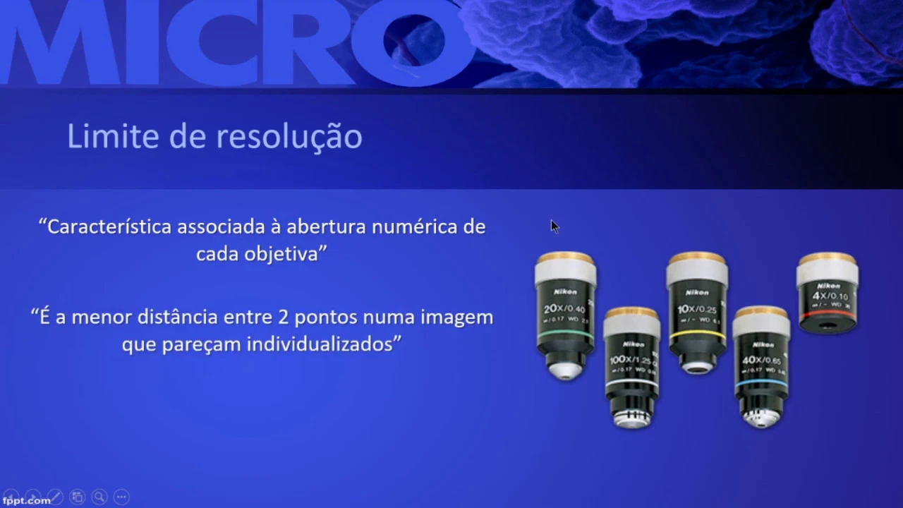
Vídeo 4.2 _ O Limite de Resolução
5.9K
Resolution in imaging refers to the clarity and detail level, measured in pixels per inch. In microscopy, resolution is associated with the richness of observable details. The limit of resolution is the minimum distance between two points that can still be distinguished as separate entities. The human eye has a resolution limit of approximately 0.2 mm, while optical microscopes improve this by about 1000 times, allowing observation down to 0.2 micrometers. The formula for resolution limit is: Limit = k × (λ / NA), where k ≈ 0.61, λ is the wavelength of light, and NA is the numerical aperture. In microscope systems, objective lenses determine resolution while ocular lenses only provide magnification. The relationship between resolution limit and detail richness is inverse: smaller limits mean greater observable detail.
Click to watch →
Prerequisite Knowledge
- Concept 01Basic concepts of intermolecular forces, particularly Van der Waals forces and the Lennard-Jones potential.
- Concept 02Hooke's Law and the fundamental mechanics of spring constants and cantilever deflection.
- Concept 03The piezoelectric effect and how it is used for precise nanoscale positioning and movement.
- Concept 04A general understanding of resolution limits in classical optical microscopy compared to scanning probe techniques.
Subsequent Learning
- Step 01Advanced scanning modes such as Magnetic Force Microscopy (MFM), Electrostatic Force Microscopy (EFM), and Kelvin Probe Force Microscopy (KPFM).
- Step 02Force-distance spectroscopy techniques for measuring mechanical properties like elasticity (Young's modulus) and adhesion at the nanoscale.
- Step 03Artifact identification and image processing methods to correct for tip-wear, sample drift, and piezoelectric hysteresis.
- Step 04Real-world applications of AFM in nanomedicine (imaging DNA/proteins), polymer science, and semiconductor inspection.
AFM Basics
Modes & Uses
AFM Basics
0:01Playing Section
- 1
Explains atomic force microscope working principle using sharp tip and cantilever.
- 2
Describes force interactions and laser detection for surface imaging.
- 3
Details scanning process using piezoelectric tube for 3D topographical data.
Limitations and Artifacts of AFM: The Case for Optical and Electron Microscopy Alternatives
While Atomic Force Microscopy (AFM) is a powerful tool for high-resolution 3D surface imaging, it has significant physical limitations that lead researchers to favor alternative techniques. AFM is notoriously slow, has a highly restricted scan size (typically under 100 square micrometers), and can damage delicate samples through tip-sample forces. Crucially, AFM images are highly susceptible to 'tip convolution'—an artifact where the geometry of the physical probe distorts the true topography of the sample, potentially leading to inaccurate surface roughness measurements. For high-throughput analysis and larger sample areas, non-contact optical techniques like Coherence Scanning Interferometry (CSI) or Scanning Electron Microscopy (SEM) offer much faster acquisition times, larger scanning ranges, and no risk of probe wear, challenging AFM's status as the sole standard for surface characterization.
Deep Dive
Advanced scanning modes such as Magnetic Force Microscopy (MFM), Electrostatic Force Microscopy (EFM), and Kelvin Probe Force Microscopy (KPFM).

Atomic Force Microscope Training: Advanced imaging modes based on oscillation, EFM, KFM, MFM, MSM
118
Advanced Atomic Force Microscopy imaging modes such as Magnetic Force Microscopy (MFM), Electrostatic Force Microscopy (EFM), and Kelvin Probe Force Microscopy (KPFM) utilize oscillation-based detection to image long-range forces (magnetic and electrical static forces) beyond the 10nm range where short-range forces dominate. These techniques employ interleave/lift mode to separate the tip from the sample, allowing detection of weak long-range forces that would otherwise be masked by stronger short-range interactions. Single-pass KFM uses multiple lock-in amplifiers to simultaneously acquire topography and surface potential data, while Frequency Modulation KFM detects resonance frequency shifts rather than amplitude changes, providing higher spatial resolution and sensitivity for imaging applications such as carbon nanotubes, graphene layers, and self-assembled molecular structures.
Click to watch →

Magnetic Force MicroscopyMFM by Dr. Surya Sharma NV
242
Electrostatic Force Microscopy (EFM) uses conductive-coated silicon cantilevers to measure electric field gradients. The grounded tip acquires topography first, then voltage is applied during lift scans. Quantification is complicated for dielectrics due to surface charges, volume charges, and tip-induced polarization. Kelvin Probe Microscopy (KPM) measures surface potential variations, applicable primarily to conductive surfaces. For semiconductors and dielectrics, image formation involves tip-induced band bending, charge injection, and contact electrification. Despite interpretation challenges, KPM enables semiconductor device profiling and failure analysis, detecting defects like electrostatic discharge-induced rupture holes invisible in topographic images.
Click to watch →

Advanced AFM Modes
208
Advanced scanning force microscopy modes—including contact mode with lateral friction for atomic resolution, non-contact/tapping modes for attractive force regimes, piezoelectric response force microscopy (PFM) for polarization mapping, conductive AFM for charge transfer studies, and Kelvin probe force microscopy (KPFM) for electrostatic compensation—are essential tools for investigating diverse material properties. KPFM, originally developed by Lord Kelvin, applies AC voltage modulation to compensate for electrostatic forces that dominate in ambient conditions, enabling true atomic resolution by balancing the tip-sample interaction potential. This electrostatic compensation is critical because ambient environments introduce water layers and surface charges that convolute measurement signals. The lecture demonstrates how these advanced modes, when properly combined and calibrated, enable researchers to achieve atomic-scale imaging, map quantum capacitance in 2D materials, study magnetic domain walls, and perform time-resolved measurements with picosecond resolution, fundamentally expanding the capabilities of scanning probe microscopy beyond conventional topographic imaging.
Click to watch →

Atomic Force Microscopy and it’s applications I Prof. Tapobrata Som I Institute of Physics
152
Atomic Force Microscopy (AFM) is a scanning probe microscopy technique that achieves atomic-scale resolution by using a mechanical probe (tip) to scan sample surfaces, with three major capabilities: force measurement between tip and sample, topographic imaging of surface morphology, and nano-manipulation for controlled material modification. AFM operates in three primary modes: contact mode (static mode) where the tip drags across the surface, tapping mode (intermittent contact) where the tip oscillates at resonant frequency, and non-contact mode where the tip oscillates without physical contact. Advanced AFM modes include Kelvin Probe Force Microscopy (KPFM) for measuring work function at atomic scale, Electrostatic Force Microscopy (EFM) for probing electrostatic forces, Magnetic Force Microscopy (MFM) for imaging magnetic domains, and Conductive AFM for measuring local electrical properties. AFM applications span materials science, nanotechnology, and device engineering, including thin film optimization, self-organized pattern formation, nanoscale functionalization, field-induced doping, resistive switching behavior, and neuromorphic computing studies.
Click to watch →
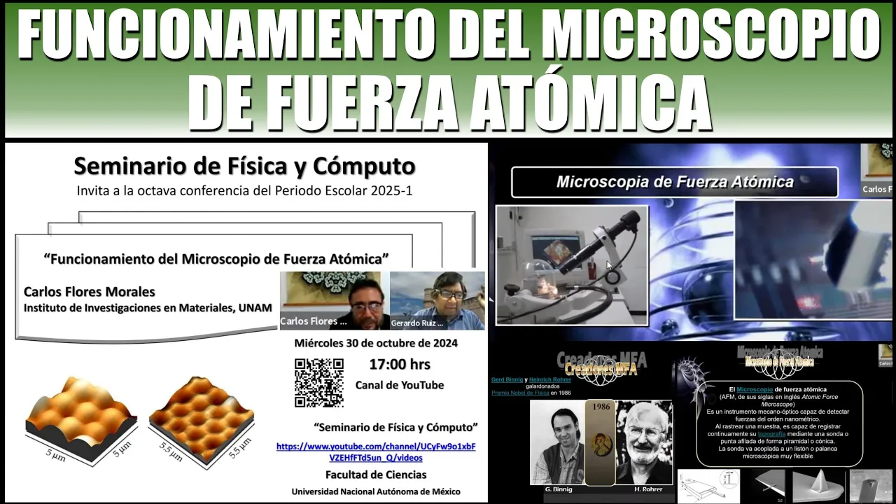
Funcionamiento d Microscopio de Fuerza Atómica (Carlos Flores Morales) Seminario de Física y Cómputo
113
AFM offers multiple scanning techniques: contact mode, intermittent contact mode, magnetic force microscopy, tunneling microscopy, lateral force microscopy, and heating/cooling capabilities. Magnetic force microscopy images magnetic domains in materials, showing grain orientations and domain structures. The presenter demonstrates imaging magnetic grains with different domain orientations. Cryogenic AFM requires liquid nitrogen introduction and vacuum maintenance, typically taking a full day to complete. Heating AFM uses current and voltage distribution to reach temperatures up to 500°C. Atomic resolution imaging reveals individual atoms and atomic lattices, though samples cannot be tilted or rotated. The technique has limitations compared to transmission electron microscopy for diffraction patterns.
Click to watch →
Deep Dive
Force-distance spectroscopy techniques for measuring mechanical properties like elasticity (Young's modulus) and adhesion at the nanoscale.

Atomic Force Microscopy (AFM) Basics Explained
58.6K
Force curve analysis enables quantitative determination of mechanical properties including adhesion, elasticity, hardness, and rupture bond lengths. The slope of the force-deflection curve during contact provides sample stiffness via Hooke's Law (F=KX). Adhesion energy is measured from the deflection at the snap-off point during retraction. Quantitative Nanomechanical Mapping (QNM) extends force curve analysis to every pixel during raster scanning, generating spatially resolved maps of mechanical properties across the entire sample surface. This technique enables correlation of mechanical behavior with other sample characteristics observed in topographical images, providing comprehensive nanoscale characterization for materials science and biological applications.
Click to watch →

Mechanical Properties of Solids+Fluids in 1 Shot | ठोसों+द्रवों के यांन्त्रिक गुणधर्म | UMMEED हिंदी
78K
Young's Modulus (Y) is defined as stress/strain for longitudinal deformation. Formula: Y = (F/A) / (Δl/l) = Fl/(AΔl). It measures the material's resistance to elastic deformation under tension or compression. Higher Young's modulus means the material is stiffer.
Click to watch →

Mechanical Properties Of Solids One Shot class 11🔥 | EAPCET 2024 | AP & TS | 🚀 Unstoppable EAPCET
81.3K
Young's modulus (Y) is the modulus of elasticity for linear stress and strain, defined as the ratio of longitudinal stress to longitudinal strain. Formula: Y = (F/A) / (ΔL/L) = FL / (AΔL), where F is force, A is cross-sectional area, L is original length, and ΔL is change in length. This measures a material's resistance to elastic deformation under tensile or compressive stress.
Click to watch →
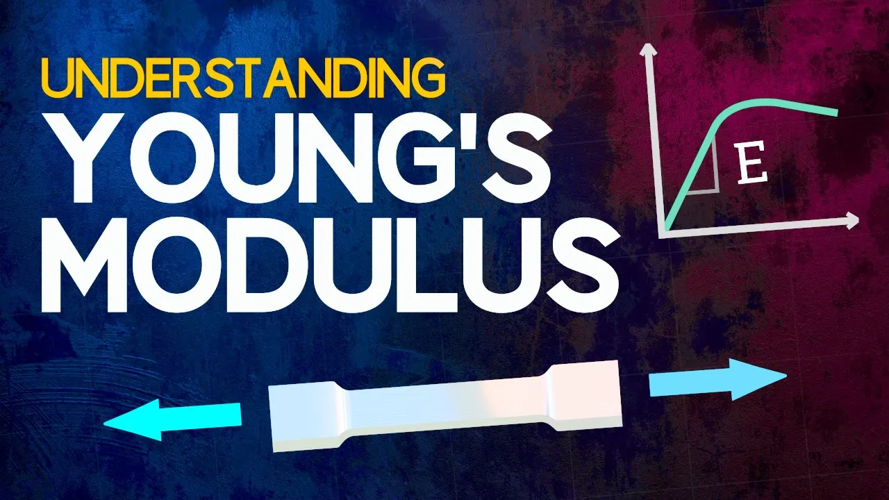
Understanding Young's Modulus
946.9K
Young's modulus (E) is a fundamental mechanical property that measures a material's stiffness, defined as the ratio of stress to strain in the elastic region of a stress-strain curve obtained from tensile testing; it represents how much a material will deform under applied stress, with higher values indicating stiffer materials that undergo smaller elastic deformations. At the atomic level, Young's modulus relates to the strength of inter-atomic bonds, which act like tiny springs resisting atomic spacing changes during elastic deformation. Different material classes exhibit characteristic Young's modulus ranges: ceramics have the highest values, followed by metals, and polymers have the lowest. This property is crucial in engineering design for controlling elastic deformations in structures like bridges.
Click to watch →

JEE: Elasticity L2 | Bulk Modulus | Class 11 | Unacademy JEE | JEE Physics | Namo Kaul
104.7K
Young's modulus (modulus of elasticity) measures a material's resistance to elastic deformation under tensile or compressive stress. It is defined as the ratio of longitudinal stress to longitudinal strain: Y = Stress/Strain = (F/A)/(ΔL/L). Elasticity varies among materials—rubber is highly elastic, while glass has lower elasticity. The elasticity of a material depends on its molecular structure and bonding. Solids generally have higher elasticity than liquids and gases.
Click to watch →
Deep Dive
Artifact identification and image processing methods to correct for tip-wear, sample drift, and piezoelectric hysteresis.

How to identify and avoid artifacts in atomic force microscopy?
468
This lecture presents a comprehensive framework for identifying and avoiding artifacts in atomic force microscopy, addressing six primary sources: probes, feedback systems, standards/scanners, image processing, vibration/noise, and sample issues. Probe-related artifacts include feature broadening (tip bluntness causes 2nm DNA to appear 20-30nm), sidewall interactions creating shadow artifacts, and tip contamination producing dragged particles. The critical rule of thumb states that accurate imaging requires tip radius to be approximately one-tenth the feature radius. Feedback system optimization requires careful PID tuning—high gain causes wavy noise, low gain produces comet-tail artifacts. Scanner artifacts include non-linearity, hysteresis, thermal drift, creep, and cross-coupling. Image processing introduces artifacts through improper leveling and filtering. Sample displacement during imaging and high loading forces cause material removal. Three verification guidelines ensure artifact-free imaging: features must scale proportionally across scan sizes, rotate appropriately with image orientation, and remain consistent across repeated scans.
Click to watch →

pa pa 10-01-2011
1.1K
Artifact tips can be damaged and this affects identification. The speaker describes an artifact that 'looks like a chisel tip but no it's broke-broke that's broke it just was real thin.' This demonstrates that damaged artifacts require careful examination to determine their original form and type.
Click to watch →

Atomic force microscopy
151
As with any imaging technique, there is the possibility of image artifacts induced by unsuitable tips, poor operating environments, or even the sample itself. Artifacts resulting from a two-course tip can be caused by inappropriate handling or collisions with a sample, scanning too fast, or having an unreasonably rough surface causing actual wearing of the tip. Due to the nature of AFM probes, they cannot normally measure steep walls or overhangs. Specially made cantilevers and AFMs can be used to modulate the probe sideways as well as up and down to measure side walls, at the cost of more expensive cantilevers, lower lateral resolution, and additional artifacts. Piezoelectric scanners are made from piezoelectric material which expands and contracts proportionally to an applied voltage—the direction depends upon the polarity of the voltage applied. The scanner is constructed by combining independently operated piezoelectric electrodes for X, Y, and Z into a single tube, or using independent stacks of piezos resulting in decoupled X, Y, and Z movement.
Click to watch →

Atomic Force Microscope AFM demo session
4.2K
Piezoelectric scanning systems exhibit hysteresis, meaning the backward and forward scans produce slightly different results due to material memory effects. To compensate for this, AFM systems acquire forward and backward scan data separately rather than combining them into a single image. If all data were combined, every second line would show an offset, degrading image quality.
Click to watch →
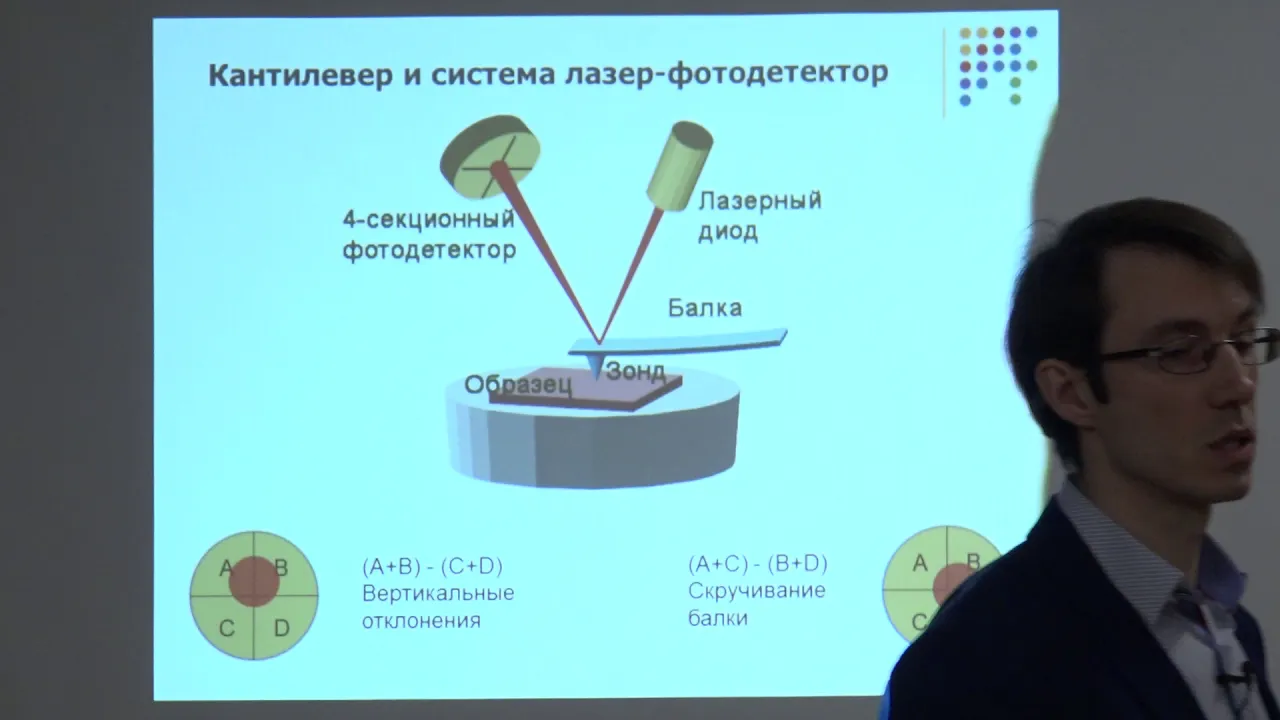
Евтушенко Е. Г. - Физические методы биохимии - 9. Сканирующая зондовая микроскопия
826
Piezoelectric materials exhibit hysteresis (nonlinear response depending on loading direction) and creep (continuing deformation after voltage stabilization). Hysteresis causes different lengths for the same voltage depending on whether the material was extended or compressed. Creep causes continued movement after voltage stabilization, distorting images. Modern instruments address these issues using feedback-controlled positioning with displacement sensors. Lower scanning speeds reduce creep effects, improving positional accuracy.
Click to watch →
Deep Dive
Real-world applications of AFM in nanomedicine (imaging DNA/proteins), polymer science, and semiconductor inspection.

Atomic Force Microscope (AFM)
2.2K
AFM has broad applications across multiple scientific disciplines including solid state physics, semiconductor studies, molecular engineering, polymer chemistry, surface chemistry, molecular biology, cell biology, medicine, and physics. Key applications include identifying individual atoms from samples, evaluating atomic force interactions, studying physical property changes in atoms, analyzing structural and mechanical properties of protein complexes such as microtubules, differentiating cancer cells from normal cells, and evaluating neighbor cell shapes and cell wall rigidity.
Click to watch →
![[유영화의 잠금해제] 계측 기술로 세계를 겨냥! 전공정에서 후공정까지 수주 터질 이 종목 / 머니투데이방송 (증시, 증권)](https://i.ytimg.com/vi_webp/Hqw69NNbUSM/maxresdefault.webp)
[유영화의 잠금해제] 계측 기술로 세계를 겨냥! 전공정에서 후공정까지 수주 터질 이 종목 / 머니투데이방송 (증시, 증권)
17.1K
Atomic Force Microscopy (AFM) is a nanoscale measurement instrument achieving magnifications of several hundred thousand to several million times, operating in air or liquid environments without special sample preparation. The non-contact scanning mode prevents sample damage, making it valuable for semiconductor wafer inspection. Park Systems holds global market leadership in industrial AFM, with 40% of revenue from Chinese semiconductor companies. The company is expanding from front-end inspection to back-end applications for 3D measurement in packaging, driven by continued miniaturization and increasing demand for precision measurement equipment.
Click to watch →
AFM - Data analysis
1.4K
AFM is important in nanoscience because it can see extremely small particles often sensitive to destructive imaging techniques. AFM can study particles at atomic resolution, seeing atom-by-atom alignment on surfaces under environmental conditions or even immersed in liquids—unachievable with other comparable resolution methods like scanning or transmission electron microscopy. AFM can study biological materials and living organisms. AFM instruments are portable and efficient, making them useful for field inspections such as fuselage inspection of airplanes. They are also valuable for investigating defects in fuel age at micro-scale levels that cannot otherwise be detected.
Click to watch →

AFM in SEM Redefining In Situ Correlative Analyses
187
AFM-in-SEM technology serves two primary application domains: (1) Material Science - low-dimensional materials, steels and metal alloys, batteries, ceramics, polymer composites, nanostructures, modified surfaces, nanostructured films, nanopatterning, and nanowires; (2) Life Sciences - morphology characterization of cells, mechanical properties measurement of proteins, and pharmaceutical research. Semiconductor applications include integrated circuits failure analysis and current leakage localization.
Click to watch →

AFM imaging of DNA related structures
369
Atomic Force Microscopy (AFM) enables direct visualization and characterization of DNA molecular structures including duplex, triplet, and quadruplex forms, which are essential for understanding cellular processes like aging, cell cycle, and cancer; AFM imaging provides biologists with valuable structural information that complements traditional biochemical methods, allowing observation of molecular assembly mechanisms and enabling the creation of DNA-based nanodevices by conjugating DNA with metallic nanoparticles for potential electrical conductivity applications.
Click to watch →
AFM Basics
Modes & Uses
AFM Basics
0:01- 1
Explains atomic force microscope working principle using sharp tip and cantilever.
- 2
Describes force interactions and laser detection for surface imaging.
- 3
Details scanning process using piezoelectric tube for 3D topographical data.
Limitations and Artifacts of AFM: The Case for Optical and Electron Microscopy Alternatives
While Atomic Force Microscopy (AFM) is a powerful tool for high-resolution 3D surface imaging, it has significant physical limitations that lead researchers to favor alternative techniques. AFM is notoriously slow, has a highly restricted scan size (typically under 100 square micrometers), and can damage delicate samples through tip-sample forces. Crucially, AFM images are highly susceptible to 'tip convolution'—an artifact where the geometry of the physical probe distorts the true topography of the sample, potentially leading to inaccurate surface roughness measurements. For high-throughput analysis and larger sample areas, non-contact optical techniques like Coherence Scanning Interferometry (CSI) or Scanning Electron Microscopy (SEM) offer much faster acquisition times, larger scanning ranges, and no risk of probe wear, challenging AFM's status as the sole standard for surface characterization.
Basic concepts of intermolecular forces, particularly Van der Waals forces and the Lennard-Jones potential.
Hooke's Law and the fundamental mechanics of spring constants and cantilever deflection.
The piezoelectric effect and how it is used for precise nanoscale positioning and movement.
A general understanding of resolution limits in classical optical microscopy compared to scanning probe techniques.
Advanced scanning modes such as Magnetic Force Microscopy (MFM), Electrostatic Force Microscopy (EFM), and Kelvin Probe Force Microscopy (KPFM).
Force-distance spectroscopy techniques for measuring mechanical properties like elasticity (Young's modulus) and adhesion at the nanoscale.
Artifact identification and image processing methods to correct for tip-wear, sample drift, and piezoelectric hysteresis.
Real-world applications of AFM in nanomedicine (imaging DNA/proteins), polymer science, and semiconductor inspection.
125.4K views1.4Klikes4:25@CaptainCorrosionOriginal Release: 2014-09-23
Trust me, I know what I'm [Applause] doing. This would happen if I try to diffuse bomb. But this is not a bomb.
This is an atomic force microscope which is used to study material surfaces. The image of the surface is obtained by standing at a very sharp tip.
When the tip is further away, then bender balls attractive forces apply between the tip and the surface.
However, if the tip is close enough to the surface, then electrostatic repulsive forces apply.
The tip is attached to a cany lever and if the tip interacts with the surface detail then the cany lever bends. The force needed to bend the cany lever is described by Hook's law where the force directly depends on the spring constant and can lever deflection. The cany lever deflection is monitored the laser beam which is focused on the cany lever and the light is reflected into a detector. If the can lever bends then the position of the laser beam changes. The surface is scanned with the sharp tip with the help of a pzo tube which can bend or stretch depending on the electric potentials applied.
The scanning can be done either by moving the sample while the tip holder is stationary or by moving the tip while the sample is stationary. This method allows to obtain three-dimensional images of the studied surfaces as each pixel also has a height coordinate.
The lateral resolution of the images is around 30 nanometers due to convolution but the vertical resolution can be up to 0.1 nm. There are three basic AFM imaging modes contact, non-cont and tapping mode. In the case of contact mode, the tip is in contact with the surface. This is good for studying hard surfaces.
In the case of non-cont mode, the tip is vibrating with a constant frequency above the surface. This mode is useful when studying soft or sticky surfaces. In the case of tapping mode, the tip is closer to the surface and vibrates with a higher amplitude. In the lowest point of the trajectory, the tip is briefly touching the surface.
The greatest advantage of AFM over SEM is the ability to study the height of surface details. This also allows measuring the surface roughness, which is very important when characterizing material surfaces. The data analysis program makes it very easy to study the sites of interest. First a line is drawn across the stud surface detail and then the height and width can be measured by simply selecting the start and end point.
Thanks for watching and leave your comments, suggestions, and questions below.
Up Next

4:03
Quantum Dots: How Size Controls Emitted Light Color
@SciToons
36.6K views•2018-06-29

12:53
21cm Hyperfine Transition in Neutral Hydrogen: Radio Astronomy Basics
@AaronRobertParsons
12.4K views•2011-10-13

32:32
NMR Spin Physics I: Zeeman Effect, Resonance Condition & Larmor Frequency
@nptel-indianinstituteofsci8064
2.3K views•2024-01-17

27:14
Entropy and the Second Law of Thermodynamics Explained
@veritasium
27.5M views•2023-07-01
Related Study Plans & Knowledge Roadmaps
Structured learning paths in Physics
physics
Nuclear Physics (Decay, Fission & Reactors)
01Atomic Structure and the Binding Force
02Radioactive Decay and Half-Life
03Nuclear Fission Mechanics and Chain Reactions
+ 2 more learning modules
12h5 modules
Explore Roadmap
physics
Soft Matter (Polymers, Colloids & Rheology)
01Foundations of Soft Matter & Thermal Forces
02Polymer Physics and Macromolecules
03Colloids, Surfactants, and Self-Assembly
+ 2 more learning modules
38h5 modules
Explore Roadmap
physics
Analytical Mechanics: Lagrangian & Hamiltonian
01Mathematical Foundations: Calculus of Variations
02From Newtonian Mechanics to Constraint Dynamics
03The Principle of Least Action & Lagrangian Mechanics
+ 3 more learning modules
28h6 modules
Explore Roadmap
physics
General Relativity (Spacetime & Cosmology)
01Foundations of Relativity: Special Relativity
02The Geometry of Spacetime: Equivalence Principle & Curvature
03Einstein's Field Equations: The Mathematics of Gravity
+ 2 more learning modules
55h5 modules
Explore Roadmap