









![10. CS50 на русском: Лекция #10 [Гарвард, Основы программирования, осень 2015 год]](https://i.ytimg.com/vi_webp/8pAFikXk1lE/maxresdefault.webp)


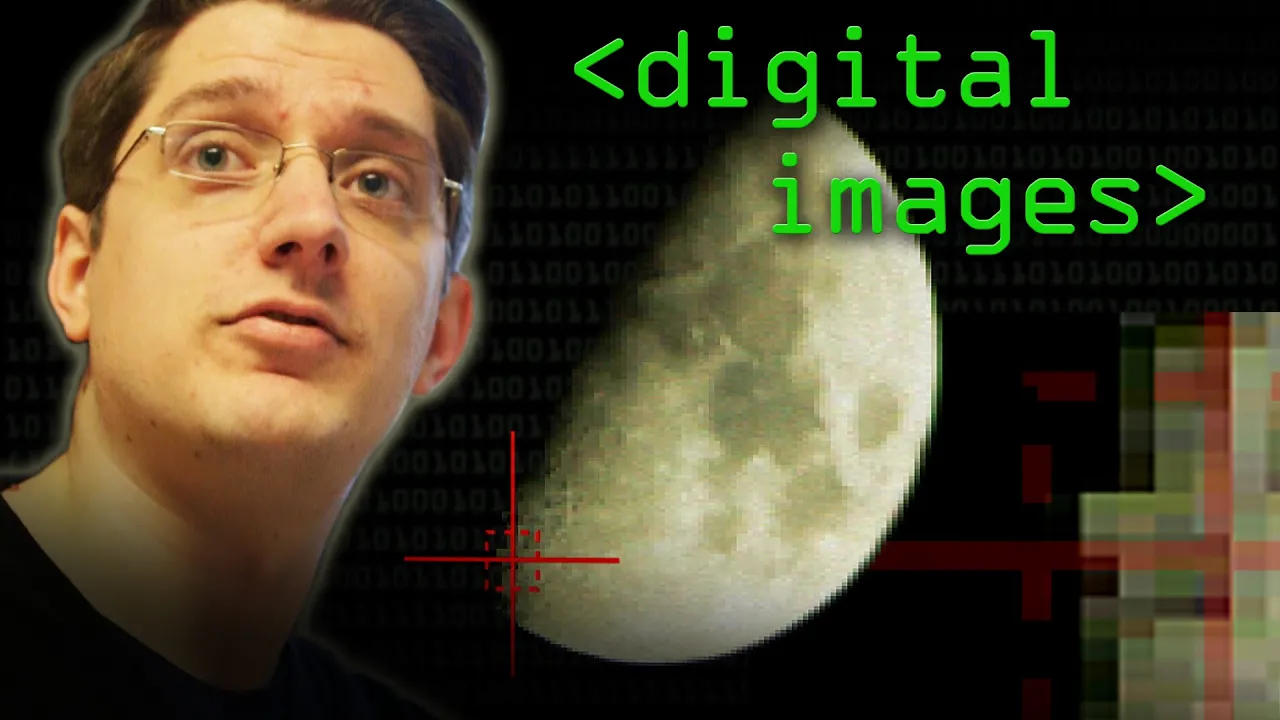
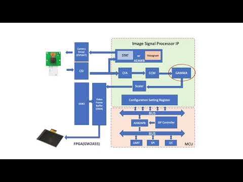

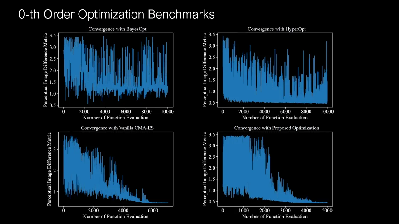











Image sensors convert light into electrical signals through silicon's photon-to-electron conversion property; CCD (Charge-Coupled Device) sensors use a bucket brigade mechanism to transfer charges row-by-row for readout, while CMOS (Complementary Metal-Oxide-Semiconductor) sensors perform electron-to-voltage conversion at each pixel, offering faster readout and region-of-interest capabilities; both technologies incorporate color mosaic filters and micro-lenses to capture and focus light onto tiny active areas, with pixel size limited by light wavelength around half a micron, pushing future development toward integrating image processing directly on the sensor wafer.
Image Sensors Explained: CCD vs CMOS | Computer Vision Basics
Added:The Photoelectric Effect: Understanding how incident light (photons) is converted into electrical charge (electrons) within semiconductor materials.
Basic Semiconductor Physics: Familiarity with p-n junctions, photodiodes, and how silicon-based components manipulate electrical currents.
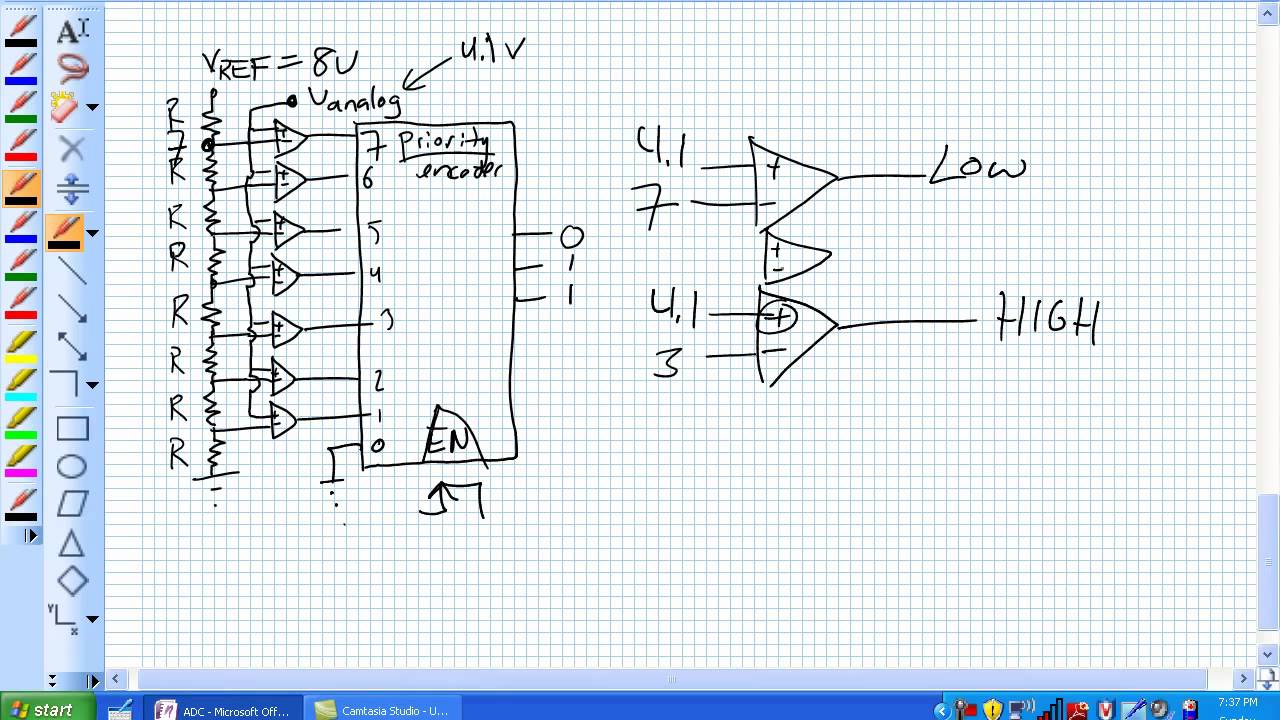
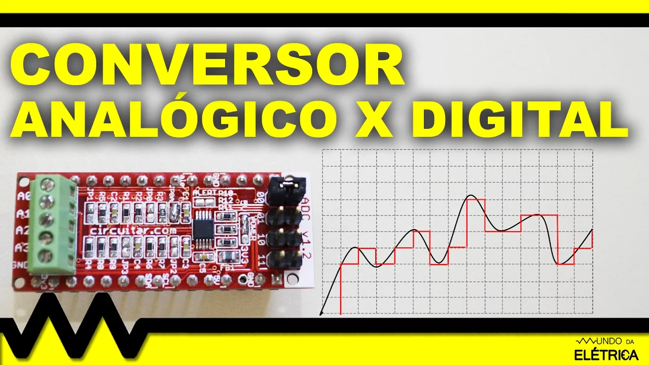
Analog-to-Digital Conversion (ADC): The fundamental process of converting continuous analog voltage signals into discrete digital representations.
Digital Image Fundamentals: A basic grasp of how digital images are represented as 2D grids of pixels with varying intensity values.
The Image Signal Processing (ISP) Pipeline: Exploring how raw sensor data is processed via demosaicing (Bayer interpolation), color correction, and noise reduction.
Shutter Mechanisms (Rolling vs. Global Shutter): Analyzing how different exposure methods affect motion blur, distortion, and high-speed capture.
Advanced Sensor Architectures: Investigating Back-Side Illuminated (BSI) sensors, stacked CMOS sensors, and SPADs (Single-Photon Avalanche Diodes).
Computer Vision Hardware Constraints: Evaluating how sensor limitations like low-light noise, dynamic range, and quantum efficiency affect downstream computer vision algorithms.
94K views2Klikes10:36Original Release: 2021-02-28
most image sensors in used today are made of silicon silicon has some amazing properties so here you see a silicon atom and when you hit a silicon atom with a photon of sufficient energy it releases an electron and what's created is called an electron whole pair so now if you have a silicon crystal that's a lce of silicon atoms and you can make this with very high Purity you hit it with light you have Photon flux coming in and you have electron flux which is being generated there's going to be an equilibrium between the photon flux and the electron flux so really silicon does most of the work for you when it comes to image sensing you hit it with light and it generates electrons and the work that remains to be done which is really challenging is to be able to read out these electrons convert them into voltage and read them out and also not to forget that you're not looking at a single Pixel just one lattice of silicon you actually have millions of pixels that you want to be able to read these charges out from and that's where a lot of the work has gone in and to create these image sensors now this is what an image sensor actually looks like this is an 18 megapix image sensor and each pixel here is roughly one micron along each of its two Dimensions 1.2 five microns in this case that's really small so you can actually pack in a 100 million pixels on an image sensor today with ease using today's technology now this isn't quite like Mo's law you know in computations according to Mo's law every 18 months you're going to be able to with the same real estate double your computational power well that doesn't happen in the case of image sensors in this case you come down to around the wavelength of light which is around say let's say half a micron once your pixel is in that region further making it smaller doesn't really help you because the resolution is now limited by this defraction effect itself the wavelength of light the size of the wavelength of light and making pixels any smaller doesn't really buy you anything so resolution will continue to grow a little bit but at some point the only way you can increase resolution is by making the chips larger and larger and we're almost there so let's talk about the first technology that's used to create image sensors this is called CCD or charge couple devices so here you see your pixels these are all your pixels each pixel has look at it as a bucket we call these potential Wells these are wells in which photons arrive and get converted into electrons so it's Photon to electron conversion and like I said before the real challenge is reading out converting these electrons into a voltage that's proportional to the number of electrons so the way CCD works is that each row actually let's take a look at this Row the photon to electron conversion happens in the pixel itself and each row passes its electron counts all its electrons to the next row and that passes it to the next row and the next row and the next one and finally comes down to this bottom row where it is read out horizontally one pixel at a time that is the electrons in each pixel are converted to a voltage right here and then this voltage is of course an analog voltage which is then converted by analog to digital conversion which is a TOD conversion to get your digital output right here so that's the process so these pixels are read out in this fashion so that sounds simple but it really is a transfer of charges from one row to the next which is a real Innovation here and this is a technique called Bucket Brigade so imagine that you have a string of people each one has a bucket of water and I would pass on my bucket to the next person and at the same time take a bucket from the person before me so that's the way Bucket Brigade actually works and so in this case how do you actually move these charges from row to row well the way you do it is you apply electric fields to appropriate positions underneath these buckets to slide or to shift the these charges from one road to the next and that is a really sophisticated piece of technology because along the way you don't want to lose any electrons and you don't want to collect any spurious electrons either so that's CCD technology and then you have camos image sensors cosos is complimentary metal oxide semiconductor another type of technology in this case again you have a potential well which where you're collecting light for instance this one right here but sitting right next to it is also Al the circuit that converts your electron to a voltage so it's a electron to voltage conversion circuit which is sitting at each pixel each pixel has its own circuit and it's not one circuit being shared by the entire chip so in this particular technology what you can do is simply address or pull one particular pixel and be able to read its voltage out so you can go to this pixel right here or you can go to another pixel and and so on and for that matter if you were interested not in the entire image but a small region in the image you can read out those uh pixels at a much faster rate because there are fewer pixels and less values to read out you can actually increase the frame rate of the cam camera substantially by just reading out that region of Interest so a lot of flexibility in the case of camos technology but the price that you pay is that now your light sensitive area that you're exposing to the world is smaller because sitting next to it you need the circuit that converts electrons to voltage so cosos and C CCD are both very popular Technologies in consumer cameras today I would say that seos technology dominates because of its flexibility and it's really come a long way in terms of its quality and there's more to an image sensor so here you see the potential Wells corresponding to pixels so this right here is one pixel this is the next pixel so that's the array of pixels and we'll call them photo diodes but then sitting on top of each one is a color filter you see a pixel doesn't really know which color is of light is arriving there it just as counting photons and so in order to measure color you're going to use color filter which sit above the pixel itself the potential well and at any given uh location you can only measure one color because again the pixel can't differentiate between colors so you use one particular filter right here let's say a red one here a green one here blue one here and after you've captured your image you can actually take these uh red green and blue values which are scattered around the image and interpolate them to figure out what red green and blue would be at each point and we'll talk about this later so those are your color filters it's called a color Mosaic and then you may be interested in knowing that each pixel actually has a lens sitting on top of it this called a micro lens this is not the lens that's forming the image what this lens does is that it just takes light from the main lens and is it focuses this this light onto the active area of the light sensitive area of the pixel which is shown down here here so this lens focuses light onto this tiny little window here and reason the reason that this window is smaller than the size of the pixel is because often like I said there's circuitry and there are leads and so on that are sitting around the pixel and you don't want to waste the light that's falling on that region so you take all the light and you Channel it down to the active area and here you see a scanning electron microscope beautiful image of the cross-section of an image sensor you see right here the micr lenses this is one micro lens for this particular pixel here you see the color filter in this case it happens to be a blue filter sitting next to it is a red filter for the next pixel and underneath that is your potential well your pixel itself where charges are being collected and circuitry to go with it and note that the distance between the top of this micr lens right here and all the way down here to the bottom of the circuitry is 9.6 micrometers so there's a lot of stuff happening there's a lot of action going on in this very thin layer of silicon and that's why I said to you earlier that you will see with the passage of time time that there's going to be more and more circuitry built underneath these so that in a single wafer you can have a perhaps image processing and computer vision happening with the image sensor layer and then your color layer and then your micro lens layer all being grown on one single wafer of silicon and in fact the main lens being grown on top of that as well this is Optics on wafer this is all coming in the decades to come
Up Next

50:20
Step-Growth Polymerization & Carothers Equation | Polymer Chemistry
@djlipomi
21.8K views•2017-04-10
30:32
Ultrasonic Transducers: Resonant Frequency Measurement and Horn Design
@imajeenyus42
229.9K views•2017-02-22
54:16
Polymer Environmental Degradation: Mechanisms & Stabilization
@iit
1.8K views•2012-07-10
33:39
How a Student's Question Saved a NYC Skyscraper from Collapse
@veritasium
22.8M views•2025-04-26
Related Study Plans & Knowledge Roadmaps
Structured learning paths in Engineering
engineering
Building Acoustic Levitators: Physics & Arduino
01The Physics of Sound and Standing Waves
02Piezoelectric Transducers and H-Bridge Drivers
03Arduino Programming: Generating 40 kHz Signals
+ 2 more learning modules
14h5 modules
Explore Roadmap
engineering
Building Peltier Cloud Chambers: Particle Tracks
01Cosmic Rays & Cloud Chamber Physics
02Thermoelectric Cooling (TEC) Fundamentals
03Custom Liquid-Cooling Loop Design
+ 2 more learning modules
18h5 modules
Explore Roadmap
engineering
Yagi-Uda Antennas: Modeling, Build & VNA Test
01Introduction to RF and Antenna Fundamentals
02Yagi-Uda Antenna Design Principles
03Antenna Modeling and Simulation in 4NEC2
+ 2 more learning modules
18h5 modules
Explore Roadmap
engineering
ECG Monitor Design: Op-Amps, Filters & Noise
01Electronics & Breadboard Basics
02Op-Amps and Instrumentation Amplifiers
03Bioelectricity and ECG Fundamentals
+ 2 more learning modules
18h5 modules
Explore Roadmap