




![Kłopotliwe ciepło [RS Elektronika] # 25](https://i.ytimg.com/vi_webp/ko9xLmW0yn4/maxresdefault.webp)








This tutorial demonstrates the complete PCB design workflow using EasyEDA software, covering schematic organization with symbols and net ports, component placement strategies, manual routing techniques with appropriate track widths for different current requirements, and exposure of copper for high-power traces. The presenter emphasizes strategic placement of connectors on board perimeters, separating high-voltage and low-voltage sections, using 45-degree angles for RF signals, and verifying designs through design rule checks before fabrication.
PCB Design Tutorial: Schematic to Layout for Inverters
Added:Fundamental understanding of DC-to-AC inverter topologies (such as half-bridge and full-bridge H-bridge circuits) and the operation of power switching devices like MOSFETs or IGBTs.
Basic familiarity with PCB design software (e.g., Altium Designer, KiCad, or Eagle) and standard concepts such as schematics, footprints, nets, and layers.
An understanding of core electrical principles related to power, specifically Ohm's law, thermal dissipation, and the relationship between trace width, copper thickness, and current-carrying capacity.
Advanced thermal management techniques for power electronics, including the calculation of thermal vias, selecting heatsinks, and utilizing insulated metal substrates (IMS).
Electromagnetic Compatibility (EMC) and Electromagnetic Interference (EMI) mitigation strategies, focusing on gate driver routing, minimizing high-current loop areas, and proper ground plane partitioning.
Designing for safety compliance and manufacturing standards, including calculating creepage and clearance distances for high-voltage isolation (IPC-2221/UL standards).
Procedures for hardware bring-up, safe testing of high-power inverter prototypes, and utilizing oscilloscopes and thermal imaging to validate design performance.
193.5K views1.4Klikes2:20:05Original Release: 2023-03-17
foreign foreign so here we are with another live stream and I know that I'm not doing too many live streams because I'm gonna be honest with you guys I'm not very comfortable speaking in English and especially in a live stream I mean I'm not comfortable in my videos where I have a script imagine in a live stream but I had this idea because I have a lot of questions anytime that I designed a PCB I got a question for how do you expose the tracks how do you make that kind of tracks how to make the PCB with this shape how to order then the PCB if it has multiple parts and so on so I thought it would be nice to just start and make a PCB start to finish make the schematic talk about how to make the schematic how to have an idea and then pass this to the schematic to a PCB design how to design the board how to select the thickness of each track I'll show you some tips and tricks and some very basic design rules and then we'll just make the PCB and also have in mind we'll be focusing later in the video about this PCB this is the PCB that I will be using by the way I'm not sure if the audio let me just check if the audio is correct here because I want to make sure yes I think we have a good audio and also definitely just make a post on Instagram because I'll share the link there so maybe more people will just come in so the post is now done and we can continue with our video and by the way I'll be also reading the comments not all the comments but some comments thank you very much if you think my English is okay I know that I'm improving it actually if you go to my first videos and as you if I should say this anyway if you go to my first videos you will see that I was just making some sort of accent and just making like a character because I wasn't comfortable with my own English but then I just change it I've changed a few words I've just got to improved I just made a lot of improvements and now I have this this is my English and I hope that you like it anyway and let's just see okay so what I was saying we'll just make a schematic start to finish and uh I'll show some tricks and some basic design rule checks and then you will just ask me ask me questions in the comment section on the chat on live stream and I will just show you that directly here because like that we can solve a lot of questions and problems so let's just start we'll be focusing on this PCB but that will be a little bit later because first we'll also over some uh very simple pcbs because I don't want to start directly with this complicated PCB as you can see we have a lot of components and it's huge by the way you have this project tomorrow now on Sunday and I don't want to make you a spoiler but you should go and see it when it will be posted because this is awesome this is one of my uh most dangerous and also very complicated project that I've made because this works with 380 volts which is very dangerous but anyway so we'll start with just start with some simple pcbs we make a schematic and then we pass through some more complicated pcbs and then finally we make this one but we won't make it uh entirely I'll just show you some tips and tricks how to make some tracks and then we pass to the already made schematic which is this one here let me just change to the desktop view this will be the schematic because I don't don't want to stay here like three or four hours when I've designed this PCB I spent like four hours entirely and only to make the tracks I think I spent like two hours so you don't want to stay here and see me how to root all these tracks in two hours so what I will do is just for example show how to make the small tracks for Signal how to make the power tracks how to expose the copper how to change the angle of the tracks and so on some basic uh placement of the components and the tracks and then we jump directly to the final schematic because otherwise we will be staying here for hours so uh first of all we will talk about the schematic and some basic rules for the schematic as well you'll want to have a schematic very well organized as you can see here I'm trying to place each part in a in a box and also I'm using a lot of these connectors to show what I want to do with these connectors for example this is a connector this is a symbol and this is a net port the idea of using net ports is to just not make lines all over your schematic I have an example here this is a schematic that I've actually downloaded for one of my projects and that was about the Nintendo based on Arduino and as you can see is a good schematic but it's very difficult to follow first of all the pins name are doubled and overlapped and you don't even know if this one is the io26 or this other one or the bottom one because the name is overlapped and at the same time if you want to just follow a tracks for example this one here if you want to see where it was connected you just follow it like this with your with your mouse and when you get here I'm not even sure if it was this one and this one because I already already got lost imagine here where you have like I don't know 10 tracks so never do this I mean it's a good schematic but as you can see it's very difficult to follow and that's why we use the net ports or the symbols so the platform that I'm using for this tutorial the tutorial is easy Eda so just go to easyeday.com you make an account and so on and I'm using this because it's free so anyone could use it but also this will be the same exactly the same for design spark LTM or any any CAD software or Spy software that you are using so as I was telling you you have to use uh the symbols or the pads let's just go over the symbols first we have for example the ground symbol and the 12 volts one you just go to the commonly library and as you can see you have the ground in VCC so let's just get this VCC here you place it on your schematic and if you want to change the name just double click the text and just call it 3.3 Watts for example imagine that you are making a 2.3 volts connection and you want to connect it to any other part of the schematic instead of just placing a line like this for example you want to connect it here this is very ugly and actually it's overlapping a lot of other parts of the schematic so you don't want that instead of doing that I just name it this 3.3 you click it you copy it you paste it where you want to have the connection and just make a connection like this so that basically is a virtual connection between these 3.3 volts and these 3.3 volts and that will go so but if you change the name here to 3.3 volts uh and instead of V just vo have in mind that this is not the same as this one because the connection is made with the name so they have to have the same name so let me just delete this this here and this here and show some real examples for example these are all ground and as you can see I'm using different grounds because sometimes you have circuits that are a little bit more complicated that will have double grounds because you have to separate the high voltage ground or the AC ground for the from the other ground in this case I was just adding a shunt I'm not sure if you can see it here are these two components and these shots are basically some very small resistors that with maybe values of 10 milliamps and you want to use these shells to measure the voltage across them and by that by dividing it by the resistance you get the current value so the ground of the 380 volts should not be the same as the ground that is connected then to the igbts which is this ground here because that would mean if I was using the same name here ground and ground it will mean that I will have a short circuit between these lines and you can measure a voltage uh drop between a short circuit you have to to have an open circuit and measure it across the resistance that's why I'm using I'm using two uh different symbols and by the way when you place a new symbol I just place it here and give it again 3.3 volts oh no let's just give it seven volts to be different and as you can see it will also create a net for me and if we go here to design manager we go to Nets we refresh and as you can see I have a 7 volts connection and the software always already tells me that there is an error with this and basically there is nothing connected to it but if I take these seven volts and maybe connect it here let's just say that I want to connect seven volts here I save it and refresh once again as you can see the error disappeared and we have the seven volts net here and anytime that you click it it will take you depending on your when your your schematic when you click it it will take you there where the connection is and if I delete it and refresh once again the seven volts connection just disappeared and that's how you can use symbols the other thing that you could use to make it very well organized are the net ports to get here get here in the menu and you have this net port here you click it once again you drop it on your schematic and give it a name let's just call it output okay so this will be an output for anything so let's just say that you want to connect this point now let's just say this point here this point here the other point that we have before let's just say that this is some sort of output you want to connect it to your driver instead of just making a line like this directly to the driver that just connected here look how ugly is and then it will create another problem this dot here and we'll talk about that in just a moment instead of doing the just that you can just copy this with the same name you can press R to rotate it in any direction you place it wherever you want on your schematic and then you make the connection to your PIN for example here and now as you can see this point is connected to this point and you don't have to pass a lot of wires and when you have this many components and this many connections you want to keep it organized because even if it's a schematic for you imagine that in the future you will be an engineer and you want to pass the schematic to anyone so they should understand it so it's very important to keep it organized and that's how you do it with symbols and with net ports obviously we have more uh symbols here we can use this one if you want you can also change the name to this one you can use the I think this one is for giving a net label so you just place it on the net and then you just change the name of that I will just call it IO and then this entire net will be called IO so I'm not really recommending this because I want to leave the software to give the name to the net however it wants and I only want to change the name of the connection so everything understood till now you want to keep it organized and also for example I use these boxes to separate the parts of the circuit when you have a circuit you will see that basically any circuit will have some sort of input otherwise it's not an electrical circuit if it would be a battery it could be it could be a power supply it will be the mains input voltage with a regulator and so on so I want to separate that for example this is the main input of the battery which basically will be these two points here I'm not sure if you can see on the webcam but this will be two connectors for the battery then I pass it to a connector here which will be a switch and like that we can turn it on and on and then this VCC is connected directly to my regulators and then The Regulators will be here because this PCB will have different values it will have 380 volts ac 280 volts DC 18 volts ac we pass it to a rectifier to 80 volt 18 volts DC we use a voltage regulator for 12 volts actually this is a regulator for 15 volts so I should change this actually we do later because this is an already made schematic and I don't want to mess it but anyway we have a regulator for 15 volts and then for 5 volts and these are connected to the rest of the circuit for example if you want to connect the 12 volts regulator 12 volts to your driver just place that icon here make the net and you have it connected and that's it actually I've made an error here just remove it and I don't want to make any errors because this is an already made schematic and I'll share with you guys the schematic this weekend when I will be posting the project of this PCB and then I'll just close it into a box like this you can just take this box tool as you can see you can draw boxes and inside you can just take the text tool like this double click it and give it any name that you want you can name it uh part one I don't know any any name that you want you can just change the site if this side this block is more important than others you can just change the the size and so on this is something that I do not all the engineers are doing this this is something for me because like this I can Orient it a little bit uh better in the schematic I know this will be the igbt part this will be the battery input we have some peripherals like the voltage feedback and the fan control this is the driver for the high frequency high voltage Transformer which is this one here so like that you can you keep the uh project organized and by the way very important when you start to start a project give it a name so the people you should know uh what project are you working on and also you can give it a version for example this is version one but if you're doing version two three you can change it here so you could keep it organized for you as well because you have different changes but different versions of the same schematic and like that you can see where you've made that change you can enter your name and the date and basically that will be a well organized schematic so now we'll start with our own schematic and I'll show you step by step how to make one and we'll do it with a very simple project so what I will do I just go to my to my website and search for a project that is using a PCB for example we can use this one but this is very simple just a few resistors let me just see here the audio play amplifier has a PCB but that's very very complicated actually I've seen here this one this was very recent this is the 433 megahertz control and I think I'll just use this one as an example we have the transmitter and the receiver and the transmitter let's just start with the receiver because it has a very interesting part because the receiver has this part here the AC to DC Transformer which is a component that you can find in Easy Eda and you'll have to make it from from scratch and I also want to show you how to create components imagine that you are designing a PCB and you don't find exactly the component that you want and you have to design it your yourself you open the data sheet you see the sizes the pad size the particle orientation and so on so you'll have to design it and we'll go over that as well so just open this in a new page and I have a double screen so what I'll do I will take this page here and pass it to my other screen because like that it will be a lot easier for me we go to easy Eda and just start a new project so we go to new project let's just call it 433 megahertz live example obviously this is just a name for me for this video but you should give it a very uh serious name related to your project and also description for example this will it it could be something like this is a project related to radio frequency connection controlling a light using an SSR Etc you can place the description here we click save and that will automatically create a us for us an empty schematic let's just wait it's not creating a schematic why not why is this not creating a schematic I did something wrong new project 433 megahertz live example and Save already exists let's this is very strange live example let me just delete this uh I can find a delete button delete this will open a project anyway it will already create a schematic for you new project 433 megahertz sorry this is a bad example a bad example bad example save it and this should there you go they should already create a schematic for you and you can just click it save and as you can see you have the project here 433 bad example and you also have the schematic which is called sheet but you can change the name to any name that you want just by double click it or modify so this is our schematic obviously uh the first step just give it the name let's just call it 433 megahertz uh transmitter receiver RX let's just place our name Electro noobs you can leave the easy 80 logo if you want but if you maybe share this with another engineer or so you maybe want to just delete this icon the date will be this one and it's the first actually this is the second one because I've already made the first one so just pick the revision here and we start placing our components but before we do that let me just check the comment section because I'm pretty sure that you left a lot of messages let me just read a few ones and if you have any questions just leave it in the in the chat box and I'll try to answer a few of those questions we have time don't worry let me just check the audio here okay the audio is quite good okay so let me just say welcome and just see what other questions we have the audio is perfect thank you just don't use I'll be back and you're fine what do you mean about that the I'll be back like Terminator for what your old videos are fine too I mean I know that the video content is okay I'm just I was talking about my accent I was making a forced accent just to cover my bad accent I was making a character that's what I was saying I was sanguinely like Russian what's up my friends will come back and stuff like that and then I just improve it and just get rid of that accent and this is how I speak English right now I'm not forcing to make any kind of accent okay what kind of software are using for PCB design usually I use this one it's Eda but I'm also using lto by the way you have a free one month free I think for students if you want and design spark I've been using design spark for like five years but that's a little bit old anyway right now I'm using easy Eda and the best part of easy Eda is the library if you click it here you can see that you have the symbols for um some of the components from LCSC which is a a company that is selling the components and you can see you can buy it directly you have this icon here you can buy the component but the best part is the user contributed so let's just put back over there without the amp Buck converter so this will be the parts of bar converter that you can find on LCSC but then you get the user contributed and these are all the parts that other users designed and shared with you so if you have a small back converter that is sold on AliExpress then just go to AliExpress for example the back converter for example this very small back converter here I'm pretty sure that you won't find a symbol schematic on LCSC for this back converter but someone designed the schematic for this one and share it with us so you go to easy Eda and in user contributed you just screw them look I think this is the same I'm not sure if this is the same now this has only two pads but if you spend a few minutes here I'm pretty sure that you will find I think this one is it has two pads here and two pets here might be this one you only have to check the size so you can place it here but actually in if you click the symbol here you're going to the symbol you get the the measure tool you click here and here and like that you will have the size this is 70 millimeters so I'm pretty sure this is not the one that we are looking here because this is very small but that you go into the size of the product which I think is this one here yes 17. I think this is this is the one then it might be this one anyway so that's the good part about easy Eda because you can find a lot of components that are not by stock by default on the library of LCSC or the or any other spark fan or so and so on any other company that is selling components because I already made modules and you can find those in here in user contributed that's one of the parts that I like about Easy Ed okay let's go to the other questions hello sir the RTC and lcdi square C directly connected them in SDA and scl there is no code for SD module I don't know what you are talking about I think you're talking about other projects but so many projects are using a nice crazy communication with SDA and SEL so I don't know what you're talking about I'm in school please listen now hahaha love your videos thank you short circuits are good a lot of flame that depends if you want to make a good projects or short circuits are not that good uh I've just I've jumped a question here the music is destructing I don't have the music I have the music oh sorry I have the music activated why why sorry for that it's just my OBS got crazy sorry about the music and it's like we've been live for like what 20 minutes right now and I just stopped the music and actually I had the music background on Loop so even if it finished it will uh repeat itself anyway let's just see any more question here is the lab recorded so we can revise if you forgot something yes this video is live right now so you can ask any question right now if you want and I will just try to answer it okay please make a tutorial about ultimate designer I am preparing that but Autumn designer is not free for anyone so the public is not that interesting I'm preparing another tutorial about Autumn designer but it should be the same as this one maybe a little bit different because they are both PCB designing software so stay tuned for that make a high voltage bldc motor controller I've already made that you mean a vfd controller or I mean a brushless motor but what is high voltage for you I think I've made one with four 48 volts and more than that what 100 volts can you increase the Audio Level a little bit of course I can and the microphone is this one and I hope that I won't jinx it properties and the microphone where is the microphone I think my microphone right now is at its maximum level and I can hear myself very well okay someone asked if I will upload this video to my channel yes this will be automatically uploaded to my channel so if you want to see it like one hour from now or maybe tomorrow you can just get to my channel and you will see it but if you want to place a question you have to do it now okay yes my my video will stay on YouTube okay so we can continue we have our design uh our schematic open we have our our PCB that we want to design which is this one here I will open a new image and just pass it on my other screen because it's easier for me and we can start designing so we add our parts the first part that I want that I like to start with is the voltage regulation part because that will be the input of our our PCB I know that my PCB will work with 12 12 volts I'm not sure if I can show you here and yes it will work with 12 volts this is a very small cell battery and I don't know that usually these are 1.5 volts but trust me this is 12 volts so I'll just grab my commonly used icons a VCC and call this 12 volts so I'll know that this will be my input and then I want to regulate these 12 volts to 5 volts because this is using the 80 tiny this is a microcontroller and this works at 5 volts so for that I just go to library and I know that the regulator that I want to use is the AMS 1117 just put ams117 we go to LCSC or glcpcb assembled and this is not the one the one the five volts one I want the AMS one one seven five volts which is this one here we click place and just like that we have our first component so and we also grab a ground icon we place it here and this PCB will have only one type of round which will be this one we use the net uh the wire tool to just add a connection between the Y the ground of the component and our ground and the v in will be 12 volts p in will be 12 volts as you can see the name of this component is quite big if you don't want to to show the entire name just Place one one one seven and like that it will be okay or ams117 and like that we have our component supplied and now we have to make another output another icon for the output the 12 volts is the input we copy this and we paste it and change this to 5 volts because this is regulated and then we place it here by the way when you are designing let me just check here to see if you when you are designing a PCB I always have with me a caliper like this one because there are some some components that on the on the designer will appear with the size button in reality they have a different size for example the battery there is no component on easy Eda or any other design that will have the exact size of the battery from here for end to here so what I will do I will just add two pads this one and this one and then when I design the PCB I measure the battery with with a caliper and just place the exact same distance between the pads or for example maybe this coil is a coil that you wind it yourself so you won't have a stock uh symbol or a PCB layout for your PCB so instead of doing that you just place two pads like this one and this one and then you measure it with your caliper and place that distance on your on your design so have in mind that having a caliper with you is very useful for example when I was designing this PCB we'll go over this as well I didn't find the exact shape for the Transformer which is this one here this Square One create this one here and the Transformer was based on this module here so what I've made was to get the Transformer out measure the distance between the pins measure the distance between the vertical alignment the size of the Transformer and I've made my own uh my own component using the caliper and then using easy Eda we'll go over that in a moment so now we have our component supplied the only problem is that it doesn't have any sort of decoupling capacitor so what I will do is to add a capacitor of 10 microfarads because I know the linear regulator is very stable but if you don't want noise you have to add some decoupling capacitors and I think this will be a 0804 is your805 sorry is a type of size SMD let's just look to SMD resistor sizes and if we open like for example this one now okay so as you can see we have zero four zero two which is very common but very small zero six zero three and zero eight zero five if you look on my on my PCB this is for example a0805 but this one is a zero six zero three and smaller than this one it will be this one is a zero six zero three smaller than this one it will be the zero four zero two but that will be very difficult to solder uh using your hand maybe if you're using solder paste I mean I can but I know that a lot of people won't be able to solder it because it's very very small for example let me just search here for multimeter this this multimeter here was using zero four zero two resistors I'm not sure if I have a picture no these are zero three zero uh zero six zero five but it also had some zero four these are zero four look how small these are I want to show you there you have it open this in a new tab then we just make a zoom so this is a zero six zero six zero three and this is a zero four zero two look how small this is it could be very difficult to solder with using your soldering iron so that's why usually I don't use zero four zero two I just go with zero eight zero five or the 10 Micro farad and if it's something smaller I will go with uh zero six zero three so just take this one we place it and rotate it with r and this will be between ground and 5 volts so what I will do just make this a little bit upwards so it will be organized where's my schematic my PCB my capacitor we place it here and what I like is to place the ground instead of just making a connection to ground I like to use more symbols like this it makes it look a little bit more organized so now we have a 10 microfarad capacitor between 5 volts and ground and let's just add a 100 Nano fret as well and this will be a zero six zero three for example this one obviously if you want to also buy the part you should check the price first this is 0.2 cents 0.2 anyway you should check the price as well replacing that here copy this paste it and just like that we have our voltage regulation and it's also sometimes recommended to place a capacitor at the input as well and where I should place that just place it here and just copy and paste the input voltage which is 12 volts and this will be also of 10 microfarads because the battery could have some Peaks so you don't want that and that's why you use a decoupling capacitor and that will be our voltage regulated part just take the box we close it in a box and I also add a text and this will be regulator voltage regulator and place it here make this a little bit bigger and we have our first part of the schematic we know that we have a battery input and then we have 5 volts output now in the picture here I told you that the battery input will be connected to two pads I haven't placed that yet so what I'll do I go to the commonly used Library I go to pets and I want the female pad which will be this one here but to be of only one pad I select that place it here I don't like the name so if you don't want to show this name I will go here we'll say displayed name we change this change it to no copy paste this because we need two pads and I'll connect one to round and the other one to 12 volts so then when we pass this to PCB this will be two pads which are this one and this one and we'll change the size of these pads and that will be our main input for our PCB so actually just select this one I like it okay yes I'm a little bit obsessed with keeping it organized actually I would change this to power input because this is the entire power input part we have the input pads the voltage regulator and so on so now I have the first part of the circuit the next part will be to add the microcontroller as I've told you this is using the 80 timing so just search for the 80 9085 as you can see designing pcbs is very time consuming you can just stay three or four hours just designing a PCB I think it's this one no 80 tiny 85 all together yes this one this is the microcontroller I will just place it here we know that this has to be supplied to the ground we copy paste it I know that has to be supplied to 5 volts copy paste it we make the connections ground will be here by walls will be up here what other connections do we have I would just check my schematic we don't have any other connection but what I'll do instead of drawing lines what I told you is to use the net port so I just copy paste it here and this will be named pb0 because that's the name of the pin copy paste it a few times copy paste it copy paste it this will be pb1 maybe two three four and five so just like that I will make the connection to my microcontroller and anytime that I copy these net ports I'll make another connection to any other part of the circuit and I'll also add a small resistor you can just use the resistor here for example just take a resistor of 0603 I'll place it here and then I'll use as an LED zero c03 LED because I want to add an LED to one of the pins this one here is just fine we add an LED we had a ground and this will be connected to pb4 so just copy pb4 and the reason that I'm adding an LED because when you want to program a microcontroller that will do something in this case this will be a microcontroller for sending radio signal you have to make sure that your list you are able to program the microcontroller so before you just program it to send the radio signals which might not work it's better to just program it to Blink on LED so this will be the LED right here would be connected to pv4 so when I get my pcbs I solder the component I test if it works if it brings the LED and that means that I am able to program that chip and then I pass through the main code so that's why I always add a resistor in series with only the resistor should be of maybe 280r to limit the current from 5 volts also at the same as with the caliper so when I design a PC I always have my caliper and also my calculator and calculator is for something like this for example 5 volts divided by 280 ohms it will be 20 like 20 milliamps of current maybe it's too much so I will just change it to 200 hours so 5 volts but divided by 200 it will be 25 milliamps which is more than enough to write zero six zero three LED so this will be our microcontroller we can just just close it in another box we can copy this text and place 80 fine 85 and that's it and now we can just move it here so it will be well organized and usually I also like to make these boxes the same size is not important but my problems and just like that we have the microcontroller as well let me just check a little bit the messages once again just to make sure that we don't have any other question and I'll get back to you back back to the schematic okay so where your where we were okay you can increase your audio a little bit I'm not sure if on why on the mobile phone the the audio is very low for example I've been I started testing with shorts videos and when I edit that video I place the audio at maximum volume on my desktop I can hear it at maximum volume but when I run the same video on a smartphone the audio is very low so it's not my problem it's something from YouTube I'm not sure why the volume is so low but I can I can listen to myself you can listen I can listen to myself so the audio is very very uh high so it's not it's not something from from me it's something for from YouTube so if you can hear me well it's not my fault sorry for that okay next question please continue the series about the smart solo charge controller yeah that was a bummer because the solar panel controller was meant to be an mppt but finally it ended up like a PID controller for voltage basically an mppt should measure the input volt the input current the output current and always try to maximize the power that goes from the panel to the battery and that project kind of did that but not perfectly and it ended up being something like a Pity controller and I want to make another one that is already made by user on YouTube but I want to improve it and use it with esp32 because it has a lot more speed and using two different uh coin sensors but my list of projects is huge so right now I'm not sure when I'll be making that project just stay tuned for that I have that on my to-do list I'm not sure when I will be able to do it okay how to design an rfpcb like Bluetooth circuits okay we should also talk about that let's just open one that uses that uses a let's open a drawer for example the B4 or the V5 I think is this one so when you design something that uses real radio frequency I've tested a lot of parts but you see you don't want to interfere this is the radio module so imagine that instead of the nrf24 you just use this a Bluetooth module which I think is also 2.4 gigahertz I'm not sure but anyway you are using a high frequency signal like for example a radio device like this one so I've made a full video about how to take care of the noise where to place the component when you're using radio first of all if you place it on top of your board make sure that the power tracks for example this is a power track this is going to a motor and using it it is using a pwm signal so basically that will turn on and off at a very high speed and that will create a lot of spikes of current spikes so very a lot of magnetic interference and a lot of noise so if you place your antenna above one of these tracks you'll have a lot of noise and you won't get any signal at the same time you also have to be sure that you add a lot of capacitors at the input so the supply of this device is very stable another problem that I find that I found is the difference between the noise of the radio antenna and the different the noise between the connection and the microcontroller the SP connection so I had a lot of noise on these tracks that are using a digital communication and not noise on the antenna so I was receiving the signal okay but the signal was getting out from the module and had a lot of noise for example these tracks are poor tracks and are passing overlapping with the spa tracks which are this one here and what they were creating a lot of noise and another one thing that you should know is that placing the module on the outside of your PCB I'm not sure if I have a PCB here but usually when I have a Bluetooth device for music for radio connection and so on I place it on the outside of the PCB because the PCB will have a lot of tracks that create a lot of noise also I was testing with adding a copper plane for example this is a copper plane here just place it on the this will be a copper plane and as you can see it can create a lot of why didn't create another nothing just make it on the bottom side round I'm not sure why it's not filling the it with copper but anyway if you fill the PCB with copper usually you should reduce the noise but I had a lot of tests and adding copper would just create more noise because it will act as an antenna for other signals and it will block the signals for the radio so if you go to 3D View as you can see there is no copper between the tracks you can just fill it and usually it should decrease the noise but not uh or the not all the times for in my case I had a lot more problems with copper plane that without copper plane I won't save it and we go to the next question please make a 12 volts 30 amps hour battery on Ultimate designer okay I had a question but I'm not sure if you just see it or just denied my question I haven't seen I'm sorry I just jumped away what is your question I need answer for low side sound bro using a sound at high side of the bridge is not the better idea for short circuit protection uh why the shunt is not the shunt is made to measure the current value is not for protection if you want protection just add the fuse and you can add a fuse at the input the positive input of your circuit in this case this is using AC input and the chantos place between the grounds because measuring the input uh if you have a loop of current measuring the current on this side or on this side is the same because the input's current is the same as the output current so the shunt is used to measure current nut as a safety feature so if you want a safety feature just add the fuse and yes it is a lot better to place it on the top side of the circuit did you read the art of the electronics no is that a book by the way I always get questions about what book you should read about PCB design about Electronics in general I I think I've read only two or three books in my whole life about electronics and I never finish those books I just read some chapters because nowadays all the information is online so if I want to find this small information instead of searching it in a book I just Google it and now we charge gbt you can find your answer in just a couple of seconds and you don't have to read an entire book if you want to read a book just to get more knowledge I'm not sure which book to recommend you because I'm not a book reader I read data sheets I read other posts on uh on the websites and so on so I can't recommend you any book okay the quality of the stream is very good and happy to hear that instead of having multiple Flags next to each other connect them together that is just my decision I mean for me this looks a lot better than connecting them together and that's how I've did it since I've started making designs and I think this is influence because my professor was doing this as well and I just copy that I mean I could just delete these grounds it will be the same just merge them together and this will be the same connection so I'm not sure if I why I do that and I also want to be at the same height I think these are just stuff that I do and is not very important I am on my laptop and my your voice is still too low but I'm not sure why it's that help otherwise that is happening I mean I mean can you hear me and these are just uh headphones the audio actually I should lower my voice because it's very the voice is very high so I'm not sure why you are listening me that low okay anyway as you can see we just continue with our schematic this will be the final schematic that we should make and instead of making the entire schematic we will be spending here like two hours what I will do is to open the original schematic which is a 400 RX yes it was the RX so this is the original schematic and for example we go back to our schematic I want to add this part here and this is a voltage regulator this is the RS schematic this is a voltage regulator that you can find on AliExpress I think it's 12 no 220 volts to 12 volts module something like that yes it's one of these modules not sure which one not this one where is that module it was blue colored right I think it's one of these ones anyway this one yeah I think it's something like this with two pins here and two pins at the output no this is the input and the output well if you find if you try to search this on the library what you would search 220 volts 12 volts inverter as you can see it didn't find any result but if you go to user contributed you might find one that suits your needs but in my case as you can see this is not exactly what I want so what I will do what I will do is just copy this edit it to fit my requirements so just clone it and you give it a name 220 volts ac towards DC module I will call it and this will get saved into my workspace so if I go to my workspace and search for it this is the the module that I've just cloned no this is the module that I'm using promise 120 volts and this is the module that I've just cloned so I will be editing this schema the the schematic symbol and the the PCB pad and then I'll import that to my schematic this is just in case that you don't find the exact shape of the component that you want to use so first let me just click the PCB schematic I think this is quite good the only change I will do is to place this at the same height that will be a lot more organized maybe place the number closer to the pad so this will be our symbol we just Ctrl s for Save we can exit this sorry for that this is our schematic and now we click the PCB pad click this here and as you can see this is not the exact shape that I want here I want two pads here and two here so you should uh get your module which I don't have right now using the calipers you measure the list ones the distance between the pads or you can find maybe a user manual of this uh symbol of this uh module with all the sizes but I know this is 29.8 by 22.
21.2 so we go to our designer and we measure that we make this to be uh 28 by 22 more or less and I know that the input will be on this side like this and the output will be on this side obviously I'm doing this very fast because it doesn't have to be perfect but in your case you should measure the distance distance between the pads and then using the measuring tool you just come here you measure it and it's uh 3.55 I think this is a 2.54 it should be so just move it around and also you can place this you can see the origin it's centered on x 2.54 so this will be at 2.54 plus the distance between the pads of 2.54 times 2 5.0 5.08 5.08 and now it as it is at the exactly the distance that we want and for y is -20 so we copy that here and now this should be the distance between the pads 2.54 you can also move these symbols here the voltage output I can rotate it this will be S Plus where is a plus output now the plus is this one so this will be the positive and this will be the negative and do the same for this one at the same height we copy and paste it ACAC also measure the distance between these pads use your caliper once again if you want to precisely know the distance and this should be this this the symbol for our component you just save it and when you save it it should you you should give it a new name converter PCB simple you save it and now we can close this symbol and if you go to library once again you will see that this component still has the same path here so what you will have to do is to place it on your schematic and here what it says footprint just click this part here it will open the footprint that it has right now which is the wrong one you don't want this and then you go to your workspace and search for the or the component that you have just edited which was this one let me just make it a little bit bigger it was this one PCB symbol you select it and it will automatically connect the symbol schematic with the PCB layout and just like that you could create any component that you want you you click applied update footprint and now this component as you can see if I refresh it has the component that I've created you can place it anywhere that you want and just like that no this is not the same one this is the one this is the one it didn't update it why not Library please not sure why not footprint search this is the PCB symbol update footprint and now it should work if I open this footprint now it's okay now it has a footprint that I wanted so just like that you can create any component that you want so let's just say that you find a transistor that it has a very special uh pad and you don't find that here so just click this schematic and you can add any other pad that you want for example just add a pad here you can make it for example it says if it if it is an SMD component you just make it instead of multi-layer top layer instead of round you can make it a polygon and maybe make it give it a size of no not polygon rectangle a size of two by one so for example this could be a pad for transistor just copy and paste it and just like that wrap and paste it this will be three by two something like that and all you have to do is to for example go to ams117 data sheet which is this one this one here and this could be applied to any other component anytime that you find a component that you don't have the pad for you can just make it your own this will be the pad and usually on any data sheet you can see the sizes and the distances between the pads as you can see here you have all the sizes of your bed you have the size of the component the distance between the pads the distance between these pads and the top of the the top pad so all you have to do is to just go here change the size of your pad and then using this one you can measure the distance between each one and place them exactly in the position that you want then you can just change to top layer still clear maybe make a square like this and that would be pretty much a component for uh for your schematic but have in mind that each pad has a number and if we open our schematic from before where it was this one as you can see this pad this pin is called one two three and four so when you make your your schematic make sure that your pads have the same name for example this is named 555 and 5. so if you want this to be one two three and four you have to change this number to one these two this was three and these two of four otherwise when you make that thing that we did before but to select the footprint of your schematic as you can see this already related that the pin one is connected to pin one the pin 2 to pin 2 the pin 3 to pin 3 and pin 4 to pin four if you add a a pad like this one that it has number five six or any other number that this symbol is having it won't rely that automatically so you have to make sure that the number of the pad on the pin of your schematic is the same as the number of the pad of your PCB schematic so just like that you could make your own uh components okay so instead of making the connections once again and lose lose a lot of time just we pass directly to the mid schematic and now if you have any question before we pass to PCB and now is the time to ask a question so let me just go here on the video so if you have any time any question about this schematico or about Connections about how to organize your schematic now is the time to make it okay uh your audio is fine okay so there are people that are hearing my audio okay and someone that is not hearing the audio okay anyway please make a video on this topic what topic what topic are you talking about if saving space is needed stick to 0603 resistors if there are multiple resistors nearby use a network resistor yes you can also find a network resistor which basically are a few resistors merged together in the same component you can also use that but I think those resistors are always the same value I'm not sure but I think that always the same value you are the best product development evangelist in the world what uh love to see your informative videos and contents thank you I'm not sure what that has to do with electronics please let me in the right direction these tips are op which are software using this is easy Eda it is a free it is a free software actually it's not even a soft I mean it's a software but it's online you just go to easy eda.com and you can work directly there to build uh efferent stepping in inverter 448 DC to 125 VC 30 amps and 5m steps efficiency please so I don't understand this type of questions because they don't have a comma and I'm not sure what you or what you want from that this how to select your physical connector size for 5 volts projects well depends on the project I mean for example for my for my multimeter no multimeter the yes the multimeter it was obvious that I wanted to make the input to be as big as possible to add this kind of connector because this was just an SMD pad connected to a metal rod so once I am in designing the PCB I can change the pad size according to what I want once again these are 0402 capacitors and resistors so I'm not sure what you want to say with that how do you select the size for your 5 volt Supply I'm not sure if you are referring to how much current that they will withstand anyway R3 should be on the other side of R4 really why is that how do you select the physical connector size for your five volts project in software I mean physical size of the connectors uh I have a cat here I think he's hungry I'm not sure what you want to say about that and this connector is a normal connector as any penis for the connectors for for the Arduino I mean go to pictures this is a typical connector a typical pin connector so anytime that you add on your software these female or male connectors it will be that size this is just one pin and you can select one two three four up to 20 pins not sure what you want to say with that what version of the Arduino IDE you are you recommend not sure let's just see what version I'm using right now I'm not sure what brush I'm using let me just open Arduino is not the latest version and I I don't want to is the 1.8.15 I don't want to upgrade my version because sometimes the libraries that I'm using will fail so sometimes I just download the downloadable zip for version of the software and just use that you've created a voltage divider with R3 and R4 so the base resistor is also syncing current into R3 when high R3 and R4 where are you seeing that R3 and R4 okay this is a voltage divider I wanted a voltage divider I wanted a voltage divider so what so this is a pull down and this resistor is connected at the base just to limit the current and it will be a voltage divider so if this is 5 volts maybe 2.5 volts will be at the base and that's more than enough because this is the BJT transistor and with the small current that will pass here it will open I'm not sure what's wrong actually this is not my schematic this is the same schematic from an SSR module and I'm sure if I can find it this one so if you take this schematic the resistor here the diode and the LED this is the same schematic as I have here on my schematic so I'm not really sure what is the problem I mean I do have a voltage divider but that's not a problem and not sure what you suggest how you would do it without this resistor here just a plain connection directly to the base of the transistor I mean you need a transistor as a pull down so when this is not connected this will be turned off and you also need a transistor to limit the current because otherwise this is a BJT and the base of the BJT is opened by the currents and you don't want to place a huge amount of current here when you want to turn it on anyway what is your opinion about Giga Arduino I haven't used it yet I've ordered one but I haven't used it yet and I've also ordered that new Arduino Nano which was called the Arduino Nano zero or something like that which is very new I also have a problem choosing the package of components for example resistors whether 20805 I'll be just back I have to open the door foreign I just received a new box and I've just received another box another bag like one hour ago with some new components and by the way I also want to make like maybe a live um mailbag video or just a mailbag video without being live where it will be just me opening components for example I just received this thing here which will be for a very interesting project stay tuned for that and what where is it these two multimeters and I'm not sure what inside of this bag it should be interesting it's not it doesn't weigh too much okay so now that we have the schematic let's just pass to PCB and learn how to make the tracks so what you'll have to do is to save your schematic we go to design convert schematic to PCB it seems that there is a problem let me just uh check the Nets here oh the problem is that I have to do schematics this one and this one so what I will do is to just delete one so the one I will delete it and now I'll go design convert schematic to PCB and now this will take all the components and place them on my PCB design what I like to do is to move them here on the side and the first thing I do is to select the size of my grid so just click here canvas properties make sure that you are on millimeters or maybe in mils but I'm not sure how much a mill is so I'm uh I'm used to using millimeters so make sure that you are millimeters I want to have a visible grid and usually I leave this as it is because 2.54 is usually the difference the distance between usual normal pins so for example these Arduino pins are 2.50 2.54 distance one to each other but if you want I also can change it to one millimeter and then the snap size the snap size is when you move a component as you can see it's it can snap into place let me just change it to a different value just make it two millimeters so each time that you move it as you can see it jumps to millimeters so that's very useful but you don't want to leave it to two millimeters because if you want to place it exactly here as you can see you won't be able because it will jump two millimeters each time so usually what I do is to make the grid size to be one millimeter and the snap size 0.1 and like that we have exactly a grid of millimeters and then each time that I move it it will move a 0.1 millimeters and that's very useful but obviously you can also leave it to 2.54 if you want the distance between the pads to be 2.54 The Next Step that I will do is to place the PCB exactly in the middle so for that you go to tools set board outline and let's just make it this size will be different when we finish the PC bead but let's just make it 60 by you know 30 30.
so the start point x will be minus 30 and the Y will be 15.
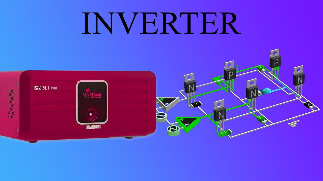
and as you can see it is exactly in the middle of the grid and that is just my way of doing the PCB design you just opened YouTube for a moment or just use a wow oh I got a three volts dial gauge and it works awesome with Arduino and ESP put an x on unused pins yes that should also be useful I'm building e-bikes and I have a 48 volts DC I need to build a stepping inverter to 125 vac to 30 amps I'm trying to ask you what type of circuit you want and how to find the schematic for stepping inverter trigger circuit well actually this PCB that will go over in a few moments this is an inverter so what you want to do first is get the voltage of your battery create high voltage in this case you want 120 volts ac so maybe you have to create 220 volts you store it into some capacitors and then using igbts you create the AC signal which could be could be a square signal or in this case it's an spwm that will create a sinusoidal signal so maybe this will help you so this weekend I'll post this project and maybe this will help you because it is a high voltage inverter from Battery it goes to in this case 220 volts ac how to decide the size of the tracks because I don't want to I don't know how to calculate it that's very easy you go to a website let me just search it PCB Trace calculator this will be so basically you have to know how much current it will extend in this case let's just say 2 amps and the thickness no I want the opposite of this I think is this one this is also useful as you can see you can enter the width the length of the thickness and it will give you the resistance I've used this website for this PCB here because I wanted to know this would be a Tesla coil stay tuned for that I wanted to know the resistance of the entire wire so as you can see this is very very long so I know that the wire is of 0.14 millimeters I know the length of the wire and also the thickness of the copper because for example if you go to pcbway.com and you go to code now as you can see you can select the thickness of the of the copper so the finished copper is just one ounce one ounce of copper so if you go to that page here you can select it to one house feet squared the length Trace let's just place it in millimeters I think it was something like 800 millimeters and the trace width was zero point when 14 millimeters and the temperature I know normal temperature of 30 degrees you click calculate and you have a resistance of 2.92 ohms that's pretty much this kind of calculator you have to use when you want to know how much current your PCB will withstand obviously in this case the track was a lot thicker because this has to withstand 500 watts so use this kind of calculator to get how uh big your your track has to be in order to withstand the amount of current that you want okay I hope that this will uh solve your question there's another page that instead of placing the size of the track you can just place the coin that you want to withstand and it will give you how thick the track should be so you have both uh both type of a website okay so let's just start the first thing that I do once I have my PCB I decide where to place the components obviously I will have an input and the then the controller output usually when you have a microcontroller you will want to place a microcontroller as Center as possible so this will be something around here and then you have the connectors on the outside you don't want to place a connector in the middle of the PCB that's that's not very clever so usually the connectors will be on the on the perimeter of the PCB so this is the input connector yes let's just say that I'll place it right here and I will hide the prefix because I don't want to see it the connector here the radio also as I told you before you will try to place it on the outside of the PCB as well because you don't want to interfere with the PCB the rest of the power connection especially when you work with high voltage so remember this module here has AC input of 220 volts and that will create a lot of noise so you want to keep your radio connection as far as possible so I'll place it here and then I'll make the PCB just a little bit bigger doesn't let me just a little bit bigger anyway I'll do later the first thing is to just select where to place the components I'll move this one as well this will be the SSR which should be close to the high voltage input just place it here we also have a button which doesn't matter where we place it just make the PCB a little bit bigger because it's too small make it of 80 minus 40.
36 and this should be 18.
just like that a PCB was too small and also if you want your PCB to be round you can just go here into tool set board outline and instead of making the round or circular just make the merge together around and circular and just place a radius of final four millimeters and as you can see now it's also around on the edges because that looks a lot cooler the radio will be here this one will be here this will be the output I'll place this output connector this will go to the load here now we place this is the LED that I've told you before should be closer to the component just rotate it just like that this will be the LED this went with a resistor which I think is this one here make sure that you place the name of the resistor so you could see it because if you place it like this when you solder the component you won't see it and this is very important because when you solder the components you will see the schematic and then your PCB and you want to see the seal player to know which resistor is is which so make sure that it is very visible and YouTube for example have two resistors close together like this make sure that you place the name in front of that resistor because for example if you place it like this if you just said something like this you don't know if this R2 is for this resistor or for this resistor so make sure that you may place it on this side or along the resistor like this in order to know which one is which the voltage regulator I place I will place this voltage regulator on the other side of the PCB so all you have to do is to select it you go here and from top layer to change it to bottom layer and it will change the color to Blue so that will be here we know that we'll have 12 Watts from here so we can place it here right like this this will have this is the diode for the control this will have an output and input capacitor this should also be on the bottom side so change it to bottom layer nope entire capacitor change to bottom layer rotate it and then the other capacitor should also be on the bottom layer I mean it's not mandatory but I want it to be on the bottom layer now we have our power supply this will be the input this will be output of 12 12 volts connected to the voltage regulator and this will give 5 volts for the rest of the electronics which will be on this side separated for all this part on the bottom will be high voltage and all this part on the top will be of low voltage 5 volts and you want to separate that and this is another diode or the control you can use these lines to know more or less where each one will go this is the transistor connected to the diode like this I'm doing this very fast because it's not very important as I told you I just want to show you more or less how to place your connection R4 will be here R5 R5 is connected to the button so just place it here like this and this is a capacitor for the radio module oh no actually this is a capacitor for the power supply so I'll just place it on the bottom side as well and guess it closer here okay just like that and these are the pads for the spa Communication in order to program it so what I will do is to hide the text because I don't care about the text and just place it very close one to each other by the way if you have any question just ask it and I'll try to make it to solve it for you okay the final PCB should be something like this so I'll place these pads on the bottom side as you can see these are the pads for programming just take them rotate them and place them maybe here and now we will have our PCB more or less I'm doing this very fast usually I would spend a lot more time but since this is just a quick tutorial and show quick tips and tricks I won't spend too much time so now you have two options first is to root it automatically and by the way for that you can just download the easy Eda pack you go to easy Eda and you download this pack here and you run this win 64 and this will make it a lot faster because this will will execute all the commands on your PC so you can just go to root and just go to automatic Auto root and when you click run it will automatically make all the tracks with the same thickness which is by default 0.25 0.25 and as you can see in just a couple of moments you finish the PCB but this is very wrong first of all as you can see we have a lot of ugly connections like this one which you don't want and second of all the program doesn't know that these are poor tracks you don't want 220 volts to pass through a 0.25 millimeter copper track you want this to be a lot thicker so let me just Ctrl Z on this one if you really want to use the automatic route you could also select some select some rules for the designer so before you run this you go to design rule check and we know to root where was the rules design rules as you can see the rule for the first the first rule is that the track the minimum track will be 0.25 the clearance is this one by the way the clearance is given by the Earth manufacturer so for example PCB way you go to capabilities you go there here down and you we should find the clearance for our PCB so memung spacing is 0.1 so you should know that the minimum space between the tracks is 0.1 in our case 0.15 so we are good to go usually I make this 0.25 0.15 the Via diameter 0.6 and 0.3 all these rules you can find them here the vehicle the track the minimum track width the mineral track clearance and so on so you can place this here but then you can make a different rule so you just add one and you call this power for example pwv double VR and this will be two millimeters thick the clearance will be four millimeter the Via diameter will be one millimeter and the drill will be 0.5 and if you want to apply this rule only to a few tracks you should select those tracks so for example the AC signal should be set to power apply and this AC signal is where to pull to power and now if I apply a setting and go once again to root auto root it will make all the tracks 0.25 but the AC signal track will be of four millimeters and you should do this for each track that you are making and I think this time it will have problems because adding a four millimeter track is very difficult let's just see it will be if if it will be able to make it it wasn't able to make it so that's why I don't use the automatic router because all it had to do is to just use a four millimeter thread like this one white doesn't let me to I think I have place the clearance of four millimeters let's just change it to two this will be two as well now I could make it that's why I didn't make it because I had a four millimeter clearance this is AC Plus why it didn't let me connect it here this is stupid change it to one I mean the distance between the tracks could be of four millimeter but the distance between the pads is not because you can change the distance between these two pads this is this is a component that already has the distance made so that's why I couldn't make the connection because when I get closer here as you can see when you click it you have some sort of circle around it and that will tell you the clearance that you have edited and if this was set to three millimeters it will touch the other pad and that's why we couldn't make the connection so instead of making an auto route what I will see what will make I will unroot them all and we go one by one so let me just teach you how you should make your manual route you click the root path the root button just make first we start with the power connection and I really want the power connection to be of four millimeters and I will leave the angle of 45 degrees you can change it to 90 but it is a lot better to make a 45 degrees especially when you are working with high frequency signals so the first part I will connect all the power so from this connector to the regulator and to the output so we start with the track we select the top layer and just like that let me just check delete the other rule because I won't use it so just like that we go like this the first connection is made and the other one something like this and as you can see I have my first connection of four millimeter we don't have enough space here so maybe I'll change this to the bottom layer so now we have four millimeter and we also have the the PCB which is made of plastic fiber in between so we have a lot of insulator insulation I'll just move this to the side like this place them a little bit here like that and the other power connection of four millimeter are between the SSR I will go on the bottom layer to change between layers you can use just these two ones we go like this one is connected and on the top layer there you go like this actually I think I'll place this on the top layer and the other one on the bottom layer and here when I change to the other layer it will automatically add the Via which is a little bit smaller so I'll change it to 1.2 and the hole will be of 0.5 for example so just like that we've made our power connection now we can go to the low power connection which will be 0.3 in my case 0.3 millimeter is more than enough and we start just routing manually and as you can see I've selected the position of the component so this will be very easy to make so just select the bottom layer here connect to the PCB to the capacitor voltage regulator this is the ground connection ground here okay for this we should make a top connection like this then we pass to the bottom side once again doing this very fast this once again will go like this the top side we add the Via like this this vrs now are too big 0.9 0.6 2.4 better yes 0.9 and 0.4 usually easy Eda if you change the size of one via it will keep making the other vs the same size so since I've changed this to 1.2 it will make this one to 1.2 as well but we don't want that because this is just a signal connection we keep routing like this anyway you see how this works so instead of suggest finishing this and lose a lot of time because it's already almost three o'clock here in Spain I would just Skip and jump directly to the PCB that I've made for this project which is this one here and on this PCB I'll explain you some tips then we go to the high power one which is this one I'll explain you some more tips and so on let's just open the other design to hide one of the layers just click here on this eye will hide the seal clear and this is the design for my PCB as you can see I've been using a three meter three millimeter tracks from the power tracks and also four millimeter in between if you want these tracks to withstand more power let me just open the 3D View as you can see we go on the back this uh this track is covered with the silk layer so this the the power will be withstained by the copper so if you want to add more copper one way to do is is to expose this track and for that just select the track that you want to expose and you can see here that we have this button here exposed copper when you click it it will automatically create a solder mask for that so when you if you save this and open the 3D viewer once again you will see that now this track is exposed so you can just get your solder and add a lot of solder on top of that actually I have a video for you let me just search it I have a video with my new project because this PCB here if we open it in 3D actually you can see it here this is the PCB as you can see it has a lot of components and this will use 500 watts so we need a lot of power to go through these tracks so instead of just ordering a PCB that is very very expensive with uh a lot of copper just expose the tracks like this one and just fill them with copper with a solder highment so I'll have a video for you where I'm filling the lines with solder let me just search it for you let's see if I can find it okay so this is the video and as you can see just take that track and add a lot of solder and like that this track will be a lot thicker and it will stand a lot more current and this is the cheapest way to do this just expose the copper and fill it with solder and the more solder you add a lot more current it current it will withstand so anytime that you want to do that just select the track that you want to make and click the exposed copper so I just expose All these power tracks we save it and now if I go to 3D View you will see that on the bottom side the portrax are exposed obviously in this case this is a very dangerous because you have exposed tracks but having us Post tracks is not more dangerous than having exposed pads with the 220 volts because if you were to touch this PCB you could touch it here the same as you would touch it here so be careful if you do this project and you are working with high voltages be very careful and make sure that you never touch the PCB while it's connected to high power actually I had a lot of bad comments on this project because a lot of people told me that this was very dangerous but you should never touch this PCB why would that would you touch such a PCB when it's connected to power usually what you will do to install this PCB is to go to your electric box just pull pull down over the the fuses cut the power for your entire home install this connect the wires install it in your wall or in some sort of insulated box connect it to your light and then turn back the power and never touch the PCB actually if you go and search for uh Alexa Alexa light switch something like that module for example this one this is pretty much the same that I have but instead of radio it also has Bluetooth and if you take a look at this this is also high voltage this is a relay for high voltage and it has a lot of exposed pads but this is a commercial product you should never touch those pads so just by making something dangerous doesn't have doesn't mean that it has to be dangerous if you work with the care with that uh component if you use it properly anyway that's why I wanted to show you how to expose the tracks what other things I wanted to show for example when you work with hiva frequency signals like the Drone this drone here any upcoming drone project uh not sure I don't think so because I had like 10 videos about drones I made the brush drones the brushless drones the Arduino drone a drone with the commercial bat flight controller the mini drone so I already have a lot of drones and a lot of radio controllers so I'm not sure if I will make a new one only if I will have a new very different idea so if you have an idea just tell me about it and maybe I will put it on my to-do list by the way this is just coffee okay so for example in for this project this is using high frequency signals so you want these tracks to be a 45 degrees because high frequency signals are getting a little bit strange when you are using 90 degrees angle so for example if you make an angle like this sorry um 0.2 if you make an angle like this high frequency won't lag this angle too much it's like a car going at high frequency and won't be able to to make the curve so usually it is a lot better to to use 45 degrees angles also and when you want to have very synchronous signals for example if you have a track like this this is connected from here to here sorry let me just change it back to 45 so imagine that you have a track like this and you have another signal that exiting uh I don't know from here and it goes like this like this like this to this point so if this signals you want these signals to get here at the exact same time and also to have the same resistance you need to make these tracks the same length as this one so usually what you will see on some pcbs is some sort of zigzag so instead of just going straight here it will go like this and make some sort of zigzag a lot let me just make again a lot more beautiful actually with 45 degrees it will be better so you can make some sort of zigzag like this this is very ugly sorry anyway I'll do this very fast because I don't want to waste any time so then the length of this one and the resistance of this track will be the same as this one so like that you will reduce the you will make the synchronization a lot faster and also the impedance of those tracks will be the same let me just search for zigzag PCB track um something like that for example this one actually this is for buttons it's not the same it's our pad for buttons so anytime that you will see a PCB that it has some sort of zigzag that's for synchronization and also have the same impedance for the track so the resistance of the track will be the same something like this anyway let's go back to our design we delete this so what I wanted to tell you is that it is a lot better to use 45 degrees instead of 90 degrees what more can I show you how to add external pads for example this pad here is not connected to now is connected to nothing and this doesn't appear on the PC on the schematic but these are just some holes of three millimeters instead in case that you want to screw this on some sort of case so all you have to do is to just click the pad button and place it here but as you can see it will give it a name it will give it a number and the name usually is ground but in this case it's nothing so if this were Ground gnd as you can see it will tell you that this is not connected so all you have to do is to change it nothing works again and change the size in my case it will be of 3.2 and the whole will be of three millimeters so as you can see this will be the pad for three millimeter screw and how to add images for example on the bottom layer let me just hide this I have this picture of my icon so what you want to do is to have the picture in a PNG format or black and white so you go to that layer in this case the bottom layer and you click the picture here and it will tell you to open an image let me just go to my my pictures and here I have this icon insert it to picture them where it is okay as you can see it's huge and just change the size 22 just making 11 by 22.
and just like that you add a picture to your seal clear and you can rotate it if you want and place it wherever you want let's just see if you have any other question I have a question during rounding do you follow schematic like from power source to capacitor to Tiny or just based on the net well when you when you want to wrote your your PCB the first step as I have as I've showed you before is to select where to place each component so for example I knew that the input will be here the voltage the converter will be here the SSR will be here and the output here and that's basic logic because you don't want to have the this component with the which is the SSR on the other side of the input that doesn't make any sense because you have to go from the input to the to the SSR and from the SSR back to the convert to the output so you have to just think more or less where to place each component so basically when you root through your tracks you will follow the schematic but at the same time you'll follow logic because you want to know uh how your track will be how short it will be the position when you want where you wanted to make uh to place it for example this track I could also pass it through here on the upside up part of the PCB but you don't want that because I want to avoid connection between the high voltage part which are these tracks and the low voltage connection of 5 volts foreign what about having insulated wires instead not as pretty but safer what are talking about insulated wires I'll talk about the exposed tracks make the connections with wires or what are you talking about someone has never worked on a power supply if they are complaining about this design yeah just just go to that video and check the comment section it was something like how can you share such as design this is very dangerous you could kill people I mean yes it's worked with 220 volts that's why I've dedicated a full minute of talking about please use proper tools never connect power while you are touching the board be very careful if you're not sure what you're doing just don't make it but this is a high voltage board so it will be dangerous so treat it with gear just because it's dangerous doesn't have to kill you if you are if you know what you are doing the exposed copper was covered by a silk mask your icon looks like a superhero you mean on this PCB no because where you have exposed track the seal clear won't appear so for example here this won't appear I'm not sure if I can show an example on this PCB yes maybe on this mosfets here let me just place the OBS so I can see the picture this mosfets here this won't focus anyway the still clear of the mosfets won't appear on the tracks because anytime that you have exposed copper like this one the silk layer won't appear on this 3D animator it will appear but on the real PCB it won't worry about that let's just see other questions is there a specific reason you prefer easy Eda and not KitKat no I've used KitKat as well I've used design spark Altium I just use this because it's very easy to use online and also as I told you at the beginning of the video I've liked the user contributed library because here you can find a lot of modules that usually don't appear in basic um PCB design software for example uh you just write I squares uh OLED which is a very common display that I use and you already have the the PCB designed for this OLED display and usually in design spark keycad or ultim you won't find that you will have to make it yourself so that's another bonus that you have with easy Eda but I don't use Easy Ada all the time sometimes I make my pcbs in Altium for example I've made this PCB coil by the way I also want to talk about this one in Autumn as well because that's a lot easier to make this round shape actually this is taking so much memory from Google Chrome sometimes it crashed because it has so many tracks that is very difficult to work with but in Altium it is a lot easier to make the circles or the spirals by the way if you want to make this you just go to your schemat to your PCB design and instead of using a normal track you click the circle one which is this one here Arc Center or this one here and you place it one here and then you sorry then you go where you want to the circle to end you place it another one here then you start here and then here that was made in spiral so just like that I'll be making the entire PCB obviously this took me once again two hours because it has like 200 spirals if you take a closer look let me just take this out as you can see it has like 200 spirals so this was a lot of work but basically that's how we can make a spiral using the arc tool if you have any other question will be this video be available to watch later yes this will be saved on my YouTube channel the sharp angle track is okay as long as the signal is below one gigahertz thank you for this tip I didn't know that it was that high I thought that with megahertz you would already have problems but I trust you so if you work with low signals like maybe one megahertz you don't have to make 45 degrees angle but for example for 2.4 gigahertz like maybe a radio connection you should work with a 45 angled signals uh tracks the HV doesn't seem as insulated with such long HV tracks yes that's also true I mean it's better to have only to have insulation over the entire board but not all the pads compared with into nothing insulated tracks all the way it is a lot more dangerous I understand that that's why on the final PCB which is this one as you can see I haven't made exports tracks Where is the the receiver PCB this one it doesn't have exposed tracks basically because it won't control that much current this works with 220 volts and the SSR the SSR here can only take up to 2 amps so with these tracks it tracks is more than enough why don't you use an x file instead of old HTML for easy Eda I don't think they have an X-File I mean it's not the next software I'm not sure if they have one that's why I'm working directly on the online version bro what is miso and mossy is Master input slave output Master output slip input those are the pins for an SP communication so if you search SPI communication as you can see we have this is the master which usually is an Arduino or a microcontroller of any kind and you can contact different slaves the aircon slaves that's an awful word for for a chip to be a slave anyway so if you want to talk to this one you enable the cheek cell chip select of this one and using the mouse and miso pins you can communicate back and forth and like that you can connect multiple slaves to the same Master that's what miso and mossy is how can I customize the board outline not like oh that's a very that's a very cool question actually the transmitter of this PCB and transmitter is this one here and as you can see it has an unusual shape so what you will do you will start let's just start with a square one let's just open file new PCB and make it 100 by 100. so if you want to take uh to make an original shape for your PCB if you go close to the outline if you make just one click it will turn white and then if you make a double click sorry like this when it's white you make a double click you will add another point and you can move this point all around so for example you can place it here and then you can make here another point and place it here and you can play with the size of the grid for example let's just change it back to one millimeter 0.1 0.1 so in this way you will know that each square is one millimeter so place it here and this one place it here so as you can see we are starting to have an original shape and for example you can move this down here this as well basically you have to add a lot of points and then place it here and here so maybe this one on the inside what happened so as you can see we're starting to have a more original shape if you want to add another point just go close double click it at another point just move it around double click it add another point just move it around and just like that you can change the shape to anything that you want for example this one here all I have to do is to just add this point here at this point here and just like that you can change this the outline to anything that you want and if you want to add for example like the FOC project look at this design let me just open it as you can see I have the outline and then another separated PCB and also on this other design I have the same exact PCB but also added some Vias so when you ask this to be manufactured you will receive this PCB and all you have to do is just just snap this PCB and break it because this part it's supposed to go over here between these pins on top of the PCB so instead of just making two pcbs and pay double the money to the PCB manufacturer I've made two pcbs on the same design so I'll send this to PCB way just as it were one PCB and then just use this vs here to break the small PCB and place it here that's another idea you could make just by setting the outline of the PCB and adding this vs here so you could break it easily now I should maybe talk about this PCB if you have any other question about the tracks I've already show you how to expose the copper so it will stand a lot more current and by the way I've told you that the connector should be on the outside you should never Place connectors in the middle of the PCB because that's very ugly and very uncomfortable to connect so the driver always in the middle or the microcontroller the connectors on the outside this is a connector for the output this is a connector for the input the capacitors the decoupling capacitor should be as close as possible to the driver because anytime that it needs power or it has a voltage Spike you need that capacitor very close to the driver so it will keep the voltage Supply very stable what other things I should tell you the track should be a 45 degrees the exposed copper is very dangerous because you could touch it what any other stuff can I tell you we'll make a DIY smps video maybe and I think I've made a power supply before with an Arduino but I'm now planning to make one with an SPS 32 which has a lot more power a lot more frequency much speed and that's the problem with my previous power supply because I didn't have enough speed so the voltage output feedback was not speed uh well it didn't have the dnf speed to control the pwm output for the controlling the mosfets and the loop was getting slower and slower but with an SPS 32 I think that I will have a lot more speed so maybe we'll have a power supply with that as well oh by the way another thing that I wanted to show you this is the 3D view of the PCB but I didn't have the capacitor I didn't have the Transformer this actually I've made this in blender I didn't have this coil here so for example you go to grabcat to grab cat let me just sign in here so this is grab cat okay what's this it doesn't work grab a grabcard website doesn't work anymore why is that okay this is graph CAD so you search for Transformer or capacitor I'm desolate dyslexic and OBG so for example you can download this capacitor here to design download file as you can see I've downloaded the 3D file for this capacitor and then when you go here in your schematic let's just say that this capacitor here doesn't have a 3D design so you go here to the 3D design now on the schematic directly this capacitor doesn't have a 3D design you click here the 3D model and you can upload your 3D model here by going to file new 3D model and here you just click add file you upload that same file that you have downloaded which is this one here but it has to be in a zip format so you just add it to a zip file no extract nap uh 7-Zip seven zip add to file I'm not seeing it anyway you upload this file here you create your own file then you go to the 3D model and you can select it from your workspace you can change the size for example instead of 18 maybe make it 22 and you adjust it to your pad and like that you will have a 3D part for your for your PCB for example this part here wasn't neither so I had to download and create a part for this sound resistor this uh driver I've also created this in blender and then just one by one you can add it for example these resistors don't have a 3D design so all you can do is just go to your PCB select this resistor go to 3D model and maybe search for resistor okay this is very small but you should find one that should uh anyway let's just say that we add this one update 3D module we save it and now when you open the 3D View you should see that that resistor that exacto resistor also has a 3D model that's how you could add a 3D model for your PCB in Easy Eda can I ask you a question about from PCB designing like your project Etc if you have any update you would like to share about the DIY microphone yes I have let me just take all the parts for that as you can see all that back there are all my projects some are finished some are not I have a lot of projects on my to-do list let me just check change here to the OBS a lot of projects on my to-do list and each of those boxes are filled with compounds that I need for a project so for example boom [Music] as you can see it says HQ microphone so high quality microphone I have all the components here I've made a lot of tests and I'm designing the 3D design to merge with this mesh because this will be the noise insulation part I have the the sound card which by the way this is very good but I will buy a new one because I found a better one and also cheaper so usually I make a lot of tests when I have those tests are okay I make a prototype usually on this kind of pcbs this is a prototype typing PCB by the way you can get this design from my for my shop on electronoops.io and just download it and send it to pcbway.com and you could have the same design and like this because it's black it doesn't have any margins because usually when you buy such a PCB from AliExpress for example prototype PCB as you can see they have these margins here and I don't like that that's why I design my own you just you can just buy it from here download the file and for just five dollars you can order this at PCB way if you want it so let me just say change to only webcam so as you can see I have all the parts in this box and once I finish with all the tests I start making the 3D design I'm still working on that design and at the same time I'm working at a different uh at different other projects but I'm not sure that this project will work I won't start recording it because as you can see I have to make a video each week so if I start a project which I'm not sure about and by the end of the week that project won't work I have to start over once again with a different project and like that I will lose a week so basically in between the projects that I record I make tests with all those projects there I make the test the Prototype the 3D design the final design and then I record it I make a script record it record the voice edit it and post it so there is a lot of work so if you want if you have any project that I once tell you that I will do and is that ready yet that's why because I have to make a lot of tests till everything is okay so stay tuned because I will have the project with the microphone ready soon I think maybe the next month I will start printing the final design and making the the project okay if you have any other question I think my cat is hungry I can hear it okay guys so basically that's how you can design bro my question uh sorry I didn't see it where is your question how can I customize the board outlined like not the regular shape I've already showed that I'll show you how to customize the board outline I just talk about that for like 10 minutes ago how do people generate the DFX file sorry I haven't seen that uh question but you are you talking about DFX DF dxf files for easy Eda or other software because for easy Eda all you have is to go to fabrication and download the Gerber files and these are the files that you send to to your to remind PCB manufacturer if you want just the vector file you can just export it as a PNG file or S SVG or this dxf file so maybe you can open this in Photoshop and edit it but usually I use PNG or or sfg and that basically here you select which layer we want to export let's export just the top layer export it and that will open a picture like this I'm not sure if it's this what you are wondering or not but you can have uh something like this in Easy Eda very very easy just export it and that's it so guys basically you have an idea you test the idea please use prototyping boards all the time such like as such as this one or the other board which right now and don't know where I placed it okay place it inside of the Box yes foreign so you have an idea you test it on a breadboard or your prototyping PCB you make a prototype if the Prototype works you can pass that final schematic from drawings with your pencil to easy Eda it will it should be something like this this will be the final schematic please use this kind of connections you make the schematic then you pass it you go to design convert to schematic you select the position of each component more or less this has to have some logic because the inputs are on the outside the micro controls on the in the middle the voltage Regulators should be close to the input of the power and so on then you decide the power the track thickness for the power and digital signals sometimes I'm using for example this is power track of three millimeters but this is also power because this is 5V Supply but this has only 0.8 millimeters and then we have the digital signal which is 0.3 so this PCB has three types of tracks three millimeters 0.8 and 0.3 you root all the tracks like this make sure that you use 45 degrees angles don't make the tracks too long be aware of the exposed copper tracks if you are working with high voltage and so on make the shape of the PCB as you wanted by just double clicking the pad and just moving the pads around and that will give a unique shape to your PCB and once you have it the final part should also be of adding a copper plane but in this case since it's working with high voltage I don't want to do that but if you want just click this button here select what kind of plane you want to add in this case I will add the ground plane just like the area like this and as you can see that will automatically add a copper plane and we can do the same for the bottom part ground once again select the area and as you can see that will add a copper plane but I don't want that because the clearance for this is at least four millimeters and as you can see if you add a copper plane the clearance is very very small so just remove that or maybe just add a copper plane here on the digital part something like this and as you can see you have still have a clearance between the high voltage and the low voltage but you have a copper plane on the digital part you can do that as you want and once you have the garbage the the final PCB you can just run the design rule check with which is the DRC and as you can see we have no errors and in case that you have an error let's just for example let's just merge this track with the top one as you can see we have an error let's just say that you have that error it will have here an error clearance you click it and it will take you to that error just solve it save it once again run the design rule check and as you can see if you have no errors you can just go fabrication gerbils download the guard bars you go to pcbway.com or any other manufacturer if you want glcpcb or any other quote now give the size I think it was 70 by 30 I only want five pcbs and this will be two layers it will be this kind of material of plastic let's just make them black calculate add your shipping your save to cart and on this page you just upload the Garbo file that you have just downloaded which are this one here you submit the order and that's it it will be approved and you can order it let me just remove this because I don't want it and just like that you will have your PCB to your home so if you have any final question before we finish this live stream you can just place it now it can be related with PCB design or my channel in general but don't worry I'll make another q a soon in a live stream and also as I told you I will make a mailbag video because I just received a new product and usually I received maybe I received like maybe 10 of these bags or boxes each week so it will be very interesting to make a mailbag and show you what kind of projects or parts I received for my projects and talk a bit a little bit about that I think that will be very interesting so tell me if you have any other question okay should we fill the rest of the PCB with copper that depends on the project I've just told you uh a few moments ago that for example if you are working with an antenna on top of your PCB it's not that good sometimes to add a copper plane because that will create more noise or even create some sort of capacitor with the antenna just have in mind that a PCB has two layers so if you have the antenna on the top layer and you have a ground layer below that will act as a capacitor because the between the copper track of the antenna and the copper attack of the plane below you have a separator which is an insulator and that will create a capacitor so have in mind for what purpose you want to add that copper plane usually I add copper planes for all my pcbs for normal pcbs for example the multimeter the multimeter is this one here and as you can see I have a copper plane it's filled with copper because in this case I don't uh I think I I try to make some changes for this PCB but anyway in this case I don't care about high frequency signals or radio signals so I add a copper plane just to be sure that I will have ground all around and so on and also remove some noise from the voltage readings so it's your decision depending on the PCB that you are designing I've learned a lot thanks for sharing I'm I'm very glad that you have learned something new bro can you give me some tips about how can we measure the quantity or the quality of fruits using some sensors and can you name some some sort of some sort of sensors well if you want to measure the quantity is very easy if you want to measure the quality that depends I think the quality is given not just by color but also by Touch by weight so that's a very difficult project I think the first the first thing that occurs to me is to use an AI with the Raspberry Pi and the camera and just record the color or the spots on your fruits like strawberries or apples and you can detect the color and by that you can sort them like this is a good fruit because it's all red or this is a bad fruit because it's not red yet it's only green and you can separate that but of course the quality the quality of a fruit is not given only by the color you have a lot of you can weight them you can measure the size maybe with some IR sensor that can measure the size between two points as you can see someone says Ace deep try using Color sensor for example but even better than the color sensor you just use a camera and just Implement an algorithm in Raspberry Pi to detect type of colors why not let free pcbs well when you shop for pcbs it's your decision on what you want to order for example the price will change so if you don't have too much money you will go with the basic one which is uh just a plastic fiberglass in between and just a normal copper hlss with lead because that's the cheapest one if you change it to lead free let's just calculate oh it's still 5 Euros I didn't know that I think if you merge it in Gold it will be 46 but lead free is eight dollars so you can you can select with lead or lead free that's that's your decision I never I didn't even knew that the lead free has the same price at the the other one and for example if you want the base of the PCB which is basically the material in between to be aluminum and actually I have things I'm not sure if you have seen in my cart that I will be ordering a PCB that is based that is made with aluminum I'm not sure if I can see it which is this one here because I'm making a a laser power meter so basically I will have an aluminum plate with a heater on top I'll place that on top of a Peltier module and this as you can see it has a lot of tracks this will get hot and I will calculate the power that this is wasting and since it's aluminum it will transfer that power into the filter module and pass that power into heat and like that you can measure the power of heat that is generated and at the same time you will have a laser pointing at this Peltier module would be will be colored in black and it will absorb that power the light power and transform it into heat and just by comparing the power that you are putting into the resistor and the part of the laser you can measure the power of the laser so I think that would be a very interesting project stay tuned for that so you can that's why I wanted to tell you that you could also select the base of the of the PCB to be aluminum but as you can see it will be a little bit more expensive instead of just 5 volt 5 volts five dollars it will be thirty dollars so depending on what you are selecting for example if you're working with very low resistances and very high frequency signals you might want to use hard gold for your pets or immersion gold but as you can see that will increase the price up to 40 40 volts to 40 dollars I'm obsessed with volts sorry for that okay what more we have here hey I just jumped the Stream hello there for anyone who just joined the Stream by the way I I'm not sure if I told you but if you make a post with Electro noobs you might appear in my live streams but it has to be on Twitter okay how do you choose about which on which side of the PCB to lay the traces and the Vias but that depends it's for me it's not important what is important is for me for me is the track thickness and to reach the point where I want to go so for example if I want to go from here to here I'll make the the track as short as possible and each time that I have to change to the other side I will change just to pass some sort of other tracks that I have in the way so if you want to make a PCB for only one layer because it's a lot cheaper you can do that but usually two layers is just five dollars so it's your decision where to play the tracks the idea is to get from this point to the other point the with the track the least amount of work and the least amount of uh the length for the track so basically that's how you in my case I select on which side of the PCB to lay the tracks okay guys so I think that we will be ending this uh live stream here because it's been like two hours I hope that you have learned something new if so consider commenting below and I'm very glad if you have learned something new have in mind that I will be making a lot of more life scenes because right now YouTube is promoting the live streams and the shorts a lot more so if you have any question I will post this video as a video or a normal video on my channel so leave those those questions below so in like that I could prepare for the future update of this uh series we'll we will be designing pcbs I know that we haven't talked too much about this PCB but don't worry because on Sunday we'll have a full tutor about this one and I'm very excited because this is dangerous this is powerful this is big and this is awesome so I hope that you like this project and I haven't seen any other project like this one on YouTube I mean I there are some projects that are using the same driver but they using uh they are using a Transformer at the output but this project is not using a Transformer as you can see this one has the high voltage creation then we have the driver the igbts the coil and the filtering capacitor at the output and this will be creating a full sine wave inverter as full sine wave at the output without any kind of Transformer and up to 500 watts and actually this could go up to 3000 Watts if you add more of these Transformers because this is the track this Transformers is the part that is limiting the the power so stay tuned for that so as I told you leave all the questions below and I will see you in the in the next live stream thank you very much and have a wonderful day and weekend keep up you guys bye bye
Up Next

52:50
A Comprehensive Guide to Soldering Eurorack Kits: Through-Hole and Surface Mount
@MoltenMusicTech
7.3K views•2020-09-23

12:54
Triumph of Orthodoxy Icon: Byzantine Art & History Explained
@BenCallan
2.1K views•2024-08-06

9:49
FastAPI vs Flask vs Django: Choosing the Right Python Web Framework
@TechWithTim
302.5K views•2024-05-26

1:42
Game of Thrones Opening Credits: A Cinematic Analysis
@gameofthrones
46.3M views•2011-04-18
Related Study Plans & Knowledge Roadmaps
Structured learning paths in General & Interdisciplinary Studies
general-studies
Elevator Engineering: History, Physics & Cities
01From Hoists to Safety Brakes: The Dawn of Vertical Lift
02Hydraulic vs. Traction: The Engineering Physics of Elevators
03Modern Speed, Safety, and Algorithms
+ 2 more learning modules
12h5 modules
Explore Roadmap
general-studies
Rubber: Material Science, History & Geopolitics
01Origins of Natural Rubber & Mesoamerican History
02The Chemistry of Natural Rubber & Vulcanization
03The Geopolitics of the Rubber Boom & Colonization
+ 2 more learning modules
12h5 modules
Explore Roadmap
general-studies
Containerization: Evolution, Logistics & Trade
01Ancient Trade & Bulk Cargo: Amphorae to Barrels
02The Industrial Revolution & Cardboard Packaging
03The Containerization Revolution: Malcom McLean
+ 2 more learning modules
12h5 modules
Explore Roadmap
general-studies
Textile Tech: Evolution, Labor & Global Impact
01Pre-Industrial Textiles: Handloom & Cottage Industry
02Mechanization: The Spinning Jenny to the Power Loom
03The Factory System & Global Labor Transformation
+ 2 more learning modules
10h5 modules
Explore Roadmap