



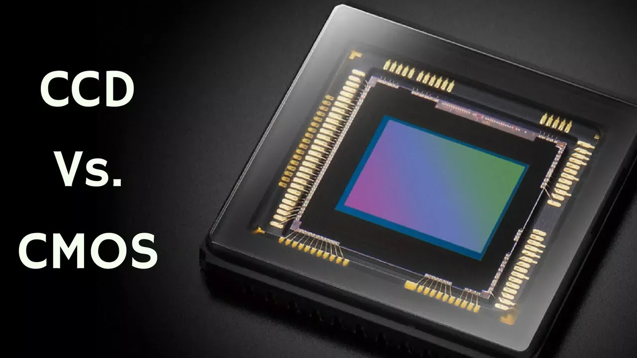











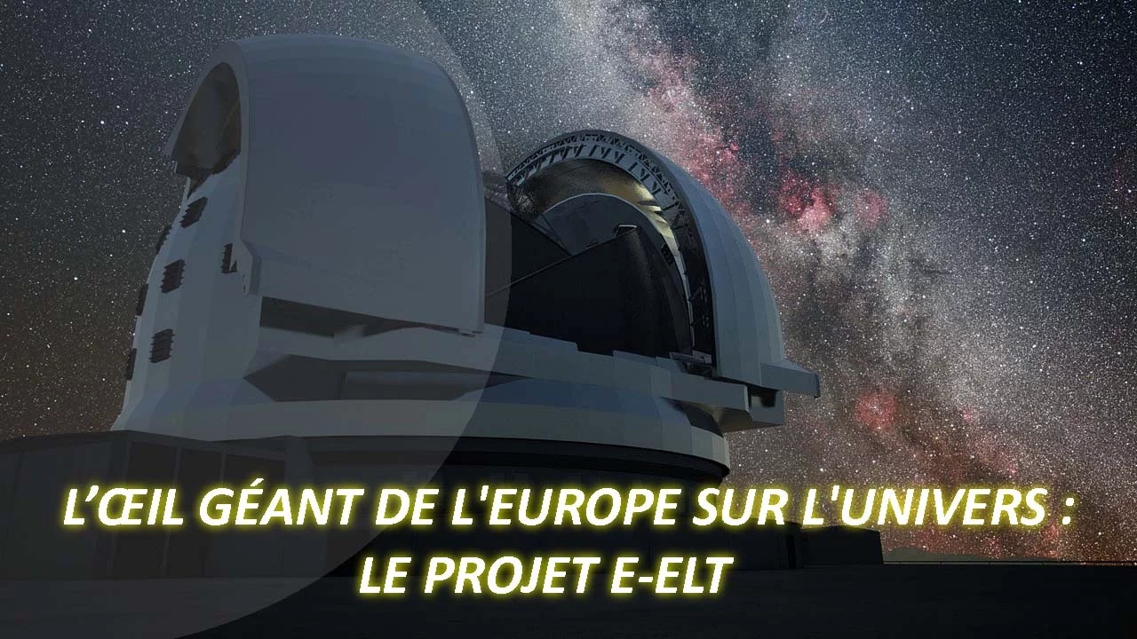







Astronomical detectors are evolving from traditional CCDs toward advanced CMOS technologies, driven by the need for lower noise, higher sensitivity, and improved performance across the electromagnetic spectrum. Ground-based observatories benefit from larger aperture telescopes (like ESO's upcoming 40m ELT) that can be built at significantly lower cost than space-based alternatives, enabling larger pixel sizes and more sophisticated detector architectures. While CCDs have historically dominated astronomical imaging due to their superior uniformity and linearity, CMOS detectors are gaining prominence because they offer sub-electron read noise, lower power consumption, and the ability to integrate complex readout electronics directly on-chip. Emerging technologies such as floating transfer gate architectures, single-photon avalanche diodes, and superconducting nanowire single-photon detectors promise to revolutionize photon-counting capabilities for future astronomical facilities. The transition represents a fundamental shift in how astronomical observations will be conducted, enabling new scientific capabilities that were previously impossible with conventional detector systems.
Future of Astronomy Detectors: ESO & Caeleste Webinar
Added:should be okay.
Okay.
Just carry on. If we carry on, Ian then.
Yeah. Okay. So, I you want me to start then? Can you can you see my slides?
Okay, everyone. Yeah, I think uh uh we can see your slides. So you can you can go I I haven't switched my I can switch my camera on but it's I mean you don't want to look at me. Anyway, good afternoon everyone and uh welcome to this webinar. I mean hopefully everyone can see the slides and they can hear me.
Okay. Uh as Ean says we're going to divide this into this webinar into two parts. First part is ESO. We're going to say what our you know what our our present needs are and what our future needs are. And we divide that into two parts where I will talk for 15 or 20 minutes and then Liz will talk for I don't know 10 or 15 minutes or whatever on future needs and then the second part is uh Ksti will talk about uh their their detectors in in optical. Now I mean hopefully you can see the slide there. I mean it's a grand title but I mean maybe some people are not aware what ESO actually stands for. It stands for the European Southern Observatory.
So our headquarters are here in Garing just north of Munich but the southern part is our telescopes are in Chile. So uh in the southern hemisphere and we do groundbased astronomy rather than that do astronomy in space and hopefully by the end of this presentation you will understand the differences between groundbased and spacebased in terms of cost and performance etc etc. Uh so if I go to the next slide so I presume that's gone on to the next slide has it? Yeah. Yeah. Okay. So as I mean Ean's already said this. So I mean this this going to be broken into two parts myself Derek Ives and Liz. Uh so and I mean I'm actually quite focused in fact I'll go to the next slide. I'm quite focused and I hate to say this on the infrared because over the last 10 years and for the first generation of instruments for our new telescope it's about a split of 70 to 30% infrared and optical. Now I can already see that we're moving towards the optical again.
So for the next the next two instruments for the VT and the VT is our 8 m telescopes. uh we have we've got an instrument called Mavis and another one called cubes which are optical based but the first generation instruments for the ELT and you'll see what the ELT is in a few minutes uh they're all infrared based uh detectors and instruments so so I will say a bit about that but then Liz will you know say what our needs are in five years hence and and further away uh so I just I mean I've got one slide here and I should I mean I I should say this and I will say this I mean about the ESO detector group itself of which both Liz and I are members. Uh so we're about 12 people strong and ESO have this thing about uh different groups whether it's a core competence or not and at ESO the detector group is a core competence and I mean again from this talk hopefully you'll see why that is over the next few slides. Uh we're a mix of electronics engineers and detector physicists and we've got people who are hard and fast detector physicist, people who are hard and fast electronic engineers and people who are a bit in between who can do some design but also know quite a bit about detectors as well. Uh but some of our hard and fast electronic engineers, they've got very very good skills on FPGA design, uh VHDL programming, even down to Linux kernel level. And then we've also got uh very good electronic designers as well. So as you'll see later on, we have to do a lot of electronic design for the hardware which goes around the detectors themselves. And then the detector physicists themselves, we've got a lot of experience with all the way from the optical, so from 330 nm all the way to the uh the long wavelengths, which in groundbased astronomy is about 20 microns. And I've got a slide in a minute to show you why that is. Uh so I mean one of the reasons we we do this is we want commonality of hardware across all our telescopes. It just makes life so much easier in for the engineers who support the the the detector systems and all the other in parts of the instruments at the telescope. But it means that for example they're going to have the same controller which controls the detector at the 8 m telescope as in our new 40 m telescope.
uh whereas there are other telescopes around the world where they allow groups to build their own hardware to do their own particular science but then another instrument comes along and even though it may have the same detector inside it's got a different detector controller controlling that detector and it makes the support problem very very difficult for the the the engineers at the telescopes. Uh so I mean I mean I've I've said that there. The other thing about is the wavelength coverage and I mean I'll go on to that slide now. So I mean why do we do groundbased astronomy at all these different wave I mean okay so there's the the scientific uh input itself but there's also the fact that the atmosphere will only transmit at at certain uh wavebands. So for example in as we all know uh optically uh from 300 to uh about 700 nanometers uh so the atmosphere transmits very well and this plot here shows transmitt transmittance of the atmosphere versus wavelength. So between uh up to one micron you can see that it it transmits pretty well and astronomers have defined these bands u to zed uh for for those optical wavelengths. And then there's also uh a J, H, and K band which astronomers call the the short wave or the near infrared.
Uh so that goes out to about 2 and a half microns. So the J band is about 1.3 microns. The H bands about 1.8. And then further on from that, there's the L and M band. So we're getting into about uh 3 to 5 microns. And then the the transmission of the atmosphere shuts from about 5 1/2 microns to about 7 1/2.
And then it opens again. And astronomers do astronomy at this band. It's they call it the end band which is about from 8 to 14 uh microns. And then it closes again. And it opens slightly at about uh 20 microns. Uh where again it's pretty tough to do but astronomers do do uh things in into Qband which is about 20 odd microns. So as you know I mean in optical we can use silicon. It's it's all to do with the band gap of the material itself. So uh so we typically we use CCDs but we're more and more looking to use CMOS devices as well but they're all silicon based and they all work from.3 to 1.1 microns. Then if we go past that into the into what I call the short wave and the the mid the mid waves. So that's from about 1 to 5 microns. Then you've got to start using different materials which have got different band gaps. And typically we use mercury cadmium teluride. Uh and I've got a more detailed picture in a minute. Uh and with the nice thing about mercury cadmium teluride, you can change the the cut off of the material. In other words, the band gap of the material itself. And then as you go very much longward, I mean from about 15 microns, you have to use different technologies again with different materials. And I'm not going to say very much about that today, but uh typically in the short wave we're using source follower per detector uh diodes uh whereas in the long wavelength we're using what are called blocked impurity band uh detectors. Uh but that that's all I'm going to say today. I mean it's very difficult to do astronomy at 20 microns on the ground and I only know of about one or two instruments around the world that actually do that.
So, okay.
Uh, I mean, I've got a slide here.
Consideration for all astronomical detectors. I mean, even though we've got bigger and bigger telescopes, and I mean, a bigger telescope means a bigger light collecting bucket. I mean, astronomers want to then look at fainter and fainter objects. So, we're always photon starved. We really are. I mean, typically, I mean, as I've said here, there might only be a few tens to a few hundreds of photons per pixel per hour.
uh from the object of interest. So very very faint objects which means you want detectors which are uh got very very low noise. So I've said we want to be read noise limited but we want the read noise to be as low as possible. We also want the detectors to be as efficient as possible in collecting the photons. So in other words we want the highest quantum efficiency and we want it to be flat across all the wavebands. And as you can see later on that's that that's not the case. uh we do want good dynamic range. So even though we want detectors with very good very low read noise.
There is a case or it happens all the time where we are in the read noise regime but there may be very bright objects on the on the same detector as well. So we want to do science with that and we want a large dynamic range where we're in the read noise regime but we're also in the shot noise regime of a very bright object.
uh we want to make the detectors as large as possible and and and usually they're two-dimensional as well. I mean the reason for that is I mean telescopes are expensive and there's very few of them. So we want to do as much science as we possibly can with the detector systems we have at at the telescope. So we want to make the detectors as large as possible so that we can look at the largest field of view. Uh and in fact you'll see later on we have multiple usually multiple detectors in our instruments as well. And then why I mean my last point here is why do we build telescopes instruments on the ground and or in space? Well, I mean on ground of course you can build much more cheaply.
So for example, I've got a a we're building a 40 m telescope at the moment and it's going to cost at least a factor of 10 if not more than the JWST which is only a 6 1/2 m telescope. So we can build something six times bigger for at least 10 times less than the cost and we can build it in much faster time scales as well and we can go and fix fix it if there are any problems. Uh the resolution that we can see depends on the on the size of the mirror. So so the ELT which is our next generation telescope is going to be 40 mters. uh so that will have a resolution which is six times better than the JWST which is the 6 and a half meter telescope that NASA uh launched a few in 2021. Uh and then I mean the sensitivity is pretty similar that's mostly due to the atmosphere itself and then when ground when we do groundbased detectors we are not really worried about radiation issues whereas they are worried about that in in space. I mean I've built instruments which have have been on telescopes for 20 odd years without any problems to the detectors themselves. Uh okay next slide. Oops sorry. Okay next slide. So just getting back to this focus of infrared detectors which I mean they they they there there is a silicon element to them but I mean basically in the short wavelength so about the 2 and a half micron and 5 micron we use these hybridized detectors. So there's a silicon so that's the picture in the top left we've got this silicon readout circuit which I'll say a bit more about in a second.
uh and I mean typically it might have 4 million pixels or 16 million pixels or or some large number and then every pixel has an indium bump on that then connects to this mercury cadmium teluride uh photo diode. So you can just about see these indium interconnects uh here and then this detector array which is this mercury cadmium turret material and then the actual if you go down I'm trying to go diagonally uh with this this this these images here. Then there you can actually see the unit cell itself. So there you can see the photo diode which is this MCT material. then the indium bump bond and then the circuitry which is in the pixel itself uh of of the detector. So typically we have very simple pixels and so you typically there's only three transistors per pixel uh so it's a very simple source follower per detector and then the next image actually shows you a bit about the how the detector is uh constructed itself.
So we use uh photovoltaic detectors. So they're diodes which are reverse biased and we use this MCT material. So this next image shows you how that connects via the Indian bump to the uh this silicon readout circuit. And then the fan image shows you a typical detector.
I mean so we're all used to seeing these things. And then the images on the top right. I mean I've got their I mean the great thing about mercury cadmium telleluride is you can change the mix of the mercury and the cadmium to change the band gap of the material. So for example if you go for a 50% cadmium then you can have a device which cuts off at about 2 and a half microns. Uh then I mean and then they've got mid- infrared.
So that's a device that cuts off at about 5.5 microns. So that's 30% cadmium. And then likewise you can go all the way I mean with mercury cabin teterate you can go all the way to 15 microns and beyond the material becomes softer and much more difficult to deal with but you can still build devices which have got uh MCT material on it and which are have a band gap which goes to 14 15 microns. Uh so I just wanted to show you a bit about the uh the devices themselves. I mean the I mean as I said they're only three transistors per unit cell. So they're they're actually very easy to operate these devices but everything the devices are completely analog. They generate a a voltage on a per pixel basis which is proportional to the number of photons that enter that pixel. And then we have to be able to address that pixel and then measure that voltage. And typically for the detector I shown you there we only need uh four clocks to do that. So we need a frame start clock, then a vertical clock which uh which increments the vertical shift register and then a a serial clock which increments the uh the serial the row register and then a clock that increments each pixel in that row itself. Uh so I mean very very simple to to uh to pro to to actually clock.
However, it means you you need to have a a system built around it that's got uh clean clocks that you've got very good control over. You also need clean biases, very very I mean electrically clean biases. I'll say a bit about that in a minute. And then you need to have very good control over the gain of your system, your electronic gain because you want to match the microvolt output of the detector to the input of your your control electronics. And then likewise you need bandwidth control and and how well you do this this digitization. Uh I just wanted to say quickly say about some about the issues with this uh MCT material. I mean MCT material is uh it's cosmetically much worse than uh than silicon material. But I mean that's because silicon has had many billions and of dollars uh thrown at it over the years over the last 30 or 40 years. were compared to MCT where it's got a ve very specific niche product which is imaging but so some of the problems I mean I've just highlighted some of the problems here so for example on the top left this is from a device which has got long wavelength material I think it goes to about 14 microns and you can just about see cosmetically that there's a lot of white uh spots on the uh on the on the material and actually this device we have rejected for for doing science because I think at least 10% of the pixels or I mean what the white pixel means is the pixel's fully saturated and you can't get any more signal into it.
Uh there's other issues. For example, on the top right we've got AC and DC cross talk. We've done a lot of work in this.
Uh so again uh the problem is the the pixel which has only got three transistors in it.
It's got quite high impedance. So you you can uh if you get uh a bright object in that in a particular pixel then you can see AC coupled versions of what's in that pixel across the other outputs of the detector. So for example the uh the device I've already quickly shown you has got 32 outputs and if you had a bright object in one of those outputs then you can see both an AC and a DC coupled version. There's different cross talk uh methods of how this cross talk happens. But here I'm showing uh examples of you've got a really bright object and then if you look to the left and right you can see ghosts of that bright broad. So they're not real astron astrometrically astronomically. How do you say that? I don't know. But I mean we've got real uh images on the on the detector but it's not real images from what the the astronomer is observing.
So, we have to uh try and get ways of getting rid of that uh or minimize it as much as possible. Uh another issue we've had recently where we've got a a 4K 4K infrared detector is we can actually see glow from the detector at the bottom of the detector. And this is the image on the middle of the bottom left where you can see this white region at the bottom and then this dark region near the near near the top and in effect the white region is glow from the readout circuitry of the detector itself. Now, we've worked very closely with the uh the manufacturer of this device over the last couple of years, and we've now managed to get rid of this glow. So, they in effect, they put more uh metallization into their into their readout circuitry to try and hide where this glow is coming from. And you can see the image on the middle of the right that the glow is gone completely. So, that's some of the issues we see with these detectors. Now, uh not much time. My goodness, this always takes longer than Be prepared, Liz. Uh, so a typical, this is the typical instrument we've now put on our on our it's about to go actually in the next month or so. This goes on the uh on our 8 m telescopes. And I wanted to give I mean there's a lot of text there which you don't need to worry about, but I wanted to give you an indication of the size of these instruments now. And on the left hand side you can just about see a a cartoon man of 2 m in height.
And the instrument is about 4 m in height. And this is only half the instrument. So uh so the instrument is almost 4 m x 4 m by 4 m. So it's they really are very large now. And this instrument here is both an optical and an infrared near infrared instrument. So it goes from I think it goes from about 700 nm all the way to 1.8 8 microns. So we've got both CCDs in this instrument and uh MCT type devices. And in fact on the image on the left you can see the three cameras. So the the detectors are in those cameras as well as the optics to focus the uh the image onto the the detector itself. And in fact the cameras you see in the left then in the middle image you can actually see the real image as opposed to the cartoon image.
And you can see two of the cameras. And then on the top right you can see these cameras which are sitting on our on an optical bench at where the where the instrument is being manufactured. And the detector system which is in the bottom right actually needs to fit into those cameras in the in the top right image there. So and as I say I mean this this this instrument is both optical and infrared. So the CCDs which are in here are typically I think they're cooled about 140 Kelvin and then the infrared detectors are cooled all the way to 40 Kelvin and all in the same instrument.
So it quite complex. Uh so if we go go on to the optical oh I mean sorry I should go back to this one. What I should say is I mean what we're trying to do is we've got six detectors in this instrument. Each is a 4K by 4K detector, but we're always trying to increase improve the efficiency of our instruments at the telescope. So in this case here, we've got actually a thousand fibers and each fiber can be positioned cuz it's on a robotic stage positioned on a on a particular object in a field. So in the ideal uh world, this instrument can look at a thousand objects uh at exactly the same time. And it's a spectrometer. So it can actually split the light from the objects and see what those objects uh with the position of them and what uh what they're made from spectra in by using the spectrums from them. Uh likewise if we now go to the optical. So again this is another fiberfed instrument. I think it's got two it's got 2,400 fibers. The instrument itself goes from the blue about 370 nmters all the way to the the near infrared. I think oh it's about 150 nanometers. So it's a uh it's on a 4 m telescope but again they're trying to get the efficiency up of doing the astronomer astronomy. So 30 years ago they might have been looking at one object but now for example they can look at 2,400 objects by using this this fiber fed under these uh these detectors. And in this example here we've got nine CCDs which are the 6K by 6K CCDs.
uh and because we want very good red response um they're deep depletion devices as opposed to uh uh high row very thick devices. So deep depletion are typically 40 microns thick and I I've tried to show you here on the right what this actually means.
So the image on the bottom right is the typical QE of these detectors. So deep depletion devices at about nine or about at one micron only has about 10% quantum efficiency. But if you can go for very thick devices which are more like 200 to 300 microns thick then you can really improve the red response of the detector. So for example on the previous instrument we have CCDs which are 300 microns thick and there at 1 micron we can typically get about 50% QE. So it's a factor of five uh improvement in throughput compared to the deep depletion devices. And again because it's a CCD we have to be very careful about the clocking of the of the devices having clean biases and then the usual about gain and bandwidth control etc. Uh okay I just want to see I'm being pushed for time already. Uh sorry Liz. I mean so I very quickly go through this. I mean a typical CCD system or sorry a typical detector system for us is the detector itself then some internal cable which goes from a cold detector at 40 Kelvin to some electronics which is cryogenic as well in our case and maybe you're asking the question later on I'll ask well why do we do that and then uh so that's the preamp you see on the on the image on the right and then the the cables from the preamp itself go to hermetic connectors on the wall of the vessel And from there there's external warm cables that go to these this warm electronics. But uh uh if I say a bit more about that well actually here this this shows this image here shows it. So here on the top left is a typical infrared detector as it comes from the manufacturer. And then in the middle top right we've we've we've removed it from the uh from its uh transportation uh case. And then on the right, we've actually got a a special tool for handling this detector. Now, I'm not going to say how much these detectors cost, but these are typically 4K by 4K hybridized detectors. So, the guys at Kilsta can understand how expensive these devices are. And then with the detector, we have to then build it into into our instrument. So, we have to be able to control the temperature.
So, uh so that's what you see on the bottom right and on the middle middle right. Sorry, the middle bottom. So, we've got you can see on the middle bottom the connectors to the detector as well as circuitry around it, which is a heater circuit and temperature control circuitry. And then on the bottom left, we've actually got circuitry then to allow us to connect the the detector to the outside world. So, we've got in this this case, this detector's got 64 outputs. So, we've got 64 uh video channels on on our and you can see this PCB in the bottom left which connects to those 64 inputs of the detector. Uh this shows it more clearly in the top left.
You can see the detector uh and then this this PC multiple PCBs which have convert the detector output to something that we can then digitize have gain etc etc. So, uh I'm not going to go into any more detail. Well, the bottom left shows you our control electronics itself. So, the detector itself is uh you can see in the middle image. So, that's the detector and then the cables which connect to it which go to the outside world. And then these cables on the bottom left connect to via 2 or 3 meters of cable to our control electronics. Uh oh my goodness, I'm really sorry. Bit pushed for time now.
Uh sorry Liz. Uh I just want to say very quickly about how we I mean detectors come tested to some minimum level by from the manufacturers. So we over the years we've spent many years building up test facilities. So for example the pictures on the right show our uh infrared detector test facility which is the the top right image and then in the bottom right sp bottom bottom right image is our test facility for CCDs. And in fact, I I've got a CCD showing there which is under test. But we can do almost everything it's needed to be done. For example, we can measure QE and absolute sense. In the optical, we use calibrated photo diodes. In the infrared, we use black bodies and the geometry of the system. And we know the throughput of the filter, etc. Uh we can do things like measure and with a CCD, we've got iron 55. So we can measure the uh the charge transfer efficiency and the uh the gain of the system ex etc etc. And maybe the last thing I should point out is we get our systems are very very low uh thermal backgrounds. So we can measure very precisely the dark current of the detectors as well because we always want to be read noise limited. So we don't want the dark current to actually overtake the read noise of the detector itself. Uh so then the detector interfacing. So I mean I mean I counted for this presentation earlier on. I mean we've got we have to interface to at least 10 different detector types which are CCDs, CMOS, infrared uh electron avalanche uh infrared L3 CCDs fully digital devices becoming more and more. So we're going from CMOS devices 3.3 volt CMOS. We've got 5 volt CMOS. We've got CCDs which typically have biases of 30 volts. We've got EAPDs which have got that the avalanche bias is typically uh 15 volts.
And then we have to go at different pixel speeds as well anywhere from 100 kHz to 10 MHz. So I'm always asked the question why do we just use AS6 uh to but I mean the the problem is we could use an ASIC for one specific detector type but then we still have to build a controller for another detector type and that's that's a very simple answer to what we really have to do. Uh and in fact I' I've got here over the years I mean I know that have been funded by by JWST for example. I mean they use the side coric it's used throughout the the instrument because they're really driven by low power uh small volume and it's in space it can never be fixed whereas that's not our driver I mean we we can we can replace boards if we have to etc in it in the simplest of cases and also I mean ESO is not ESAS so our budget's a lot smaller so actually developing AS6 etc would be a large part of our our our funding as a detector whereas we'd rather be spending the money on the detectors themselves.
Uh so I'm I'm I'm going to jump ahead here now. So over the years, over the last 20 years, actually in my time, we we've gone through at least three iterations of detector controllers which can run CCDs or EAPDs or or CMOS detectors or now even uh digital CMOS devices. So uh I mean and now our most recent iteration which is we've only got it going in the last year or so but it's more and more becoming based on uh offtheshelf components. So and for example NGC2 which is what we call this this new system is based on microtca which is an industrial standard used by a lot of telecommun telecommunication companies but also used a lot in the particle physics community as well. And uh we've also got a lot of in in the past we could define our own uh interface standards but now we more and more for our new next generation of instruments and telescopes we want to use industrial standards. So for example we're using 10 GB Ethernet we're using 1 gig of Ethernet for uh for the time protocol etc etc and uh I think Liz over to you really I need to stop there.
Okay. Um Derek, there were a few questions. Yeah, there were a few questions that came up. Um so, uh one, um was to do with the type 2 super lattice detectors for the mid and very long IR detectors. Um I think maybe I can actually just take the answer to that one, which is that um that's a wonderful new material that enables good performance at high operating temperature. But uh for groundbased astronomy, we basically have as much power as we want. So um we can cool down to very low temperatures and take advantage of the performances advantages of MCT at those temperatures. Um there was also a question about uh detectors with spectral resolution capabilities. So I will briefly touch on that in my next section. So I'll leave that.
Um, and then, uh, somebody asks, um, I'm really impressed that the controller design has evolved to support all these types. Has the design been challenging to adapt to these new and different types of detectors?
Uh, I mean, I I would say that even though we're using C's hardware, we still have to design bespoke boards for each detector type. So, for example, we're now operating EAPDS, MCT material, and CCDs from the controller. But for each of those detector types, we've had to design specific boards for those detectors. And in the next few months, we've got a fully digital detector that we want to run from the controller. And we're going to have or we've already designed a board which interfaces to that fully digital controller. But software wise and and 10 GB Ethernet wise, even though there's different detector types connected to the controller, they all look the same to the astronomer.
Okay. And the next question was uh what is the reason for the glow issues in the MCT detectors? Uh it I can I can say a lot but I'm not I don't think this is the time and place now. Okay. Um and then there was another question. Are H4RG classified as groundbased and space-based like the H2RG?
Uh I believe they are. Yeah. I mean well there's the H4RG which has got 10 micron pixels which is definitely going in which is in the Nancy Roman telescope.
Uh I I assume the 15 micron pixel can go into space as well.
Okay, great. Then um I will share my part of the slides and I will start talking. I hope that is the presenter view. Yes, people can see that.
Excellent. Okay, good. So Derek talked about what we are working on currently right now at ESO, but um I am also looking a bit to the future of what we're going to be doing in the next five to 27 years until I retire and then it's uh the next person's problem. Um so I guess the the main point is that the ESO detector group mostly serves instrumentation program. And what this is is it's the program within ISO that develops instruments for all of ISO's optical and infrared telescopes. So this includes the VT, the VTI, which is the interferometer, uh Vista, the survey telescope, and the extremely large telescope, as well as some other smaller telescopes that exist um at sites around ESO for instruments that are currently in development. So I just included the ones here that are currently in the design phase or the MIIT phase. Um but there are many more instruments that have been built by ESO and there are even more coming on the horizon. Um just quickly to go through these. Mavis is an extreme AO imager for the VT that will be in the visible. Mosaic is a multiobject fiberfred specttoraph that will go on the ELT. So very high resolution um and covers the visible and the infrared. Andes is an ultra high resolution a shell spectrograph in the infrared. Um and that's uh to resolutions of 80,000. So this is something that is um you know it's a sort of unique capability in the suite of instruments at ESO. Um blue muse is a wide field integral field spectrograph in the UV and blue. Um this allows you basically to take an image and for every image you get a spectrum. Um this is done using complex optics um image slicers as opposed to energy resolving detectors. I'll talk briefly about that in a bit.
Um, then there's ELTPCS. Sorry, I didn't find a logo for that one. Uh, that will be the extreme AO imager and chronograph for the ELT. The goal is to characterize exoplanet atmospheres. Um, Harmony is an infrared integral field spectrograph on the ELT. Um, again, getting a spectrum for every single pixel you see in an object. Medis is the mid- infrared spectrograph for the ELT that actually goes out all the way to Mband which Derek uh mentioned to you. Cubes is an ultraviolet spectrograph for the VLT and Maccato is the infrared AO imager for the ELT. Um and that will have a image resolution of 4 millarch seconds. So these are the these are the current ones that we are working on in the group right now. Um, our requirements for these instruments are generally quite similar to the previous instrument developments done at ISO and our driving requirements are large pixels because our telescopes are huge and you simply just can't cram all of that light into a single pixel, right? So, uh, the optics term is conservation of a omega. So, for a 40 m telescope, um, you need to get all the light down into a 10 to 15 micron pixel. We also want very low read noise, low dark current and high quantum efficiency. Um, and for all of these instruments that are visible, we've completed the design, the ones that have completed the design phase have actually selected CCDs, um, which has been the standard for the last decades. Um, and the IR ones have selected um, the hybridized MCT detectors for the J3M band. So in some sense the next generation that is going to go on the telescope next sort of are using the same technology we've always used.
However some of the instruments that are still in the design phase are actually trying to investigate some novel alternatives. Um and this is where CMOS detectors enter the picture and also curvature of the detectors.
So one thing that has really sort of sparked the interest of astronomers is that um if you look at the sort of CMOS market world right now there's a ton of effort moving towards sub electron read noise um and this is you know basically a huge benefit because in a photon star situation you're almost always read noise limited. So if you can push this lower basically you can gain telescope time back is how that works. Also with CMOS, you may require less cooling to reach the same uh performance levels as CCDs, especially in dark current, which then gives you the opportunity to simplify your cooling systems on your on your instruments. And also, of course, CMOS runs with lower clock voltages and biases with simpl which simplifies the controllers um significantly. And then the other thing that's happening with these fiberfed spectrographs is basically just due to size and the numerical aperture of the fibers uh coming from the instruments you have fiber cores around 160 microns and you need to get all that light into as few pixels as possible. So you build really fast cameras um you know below f1 which then in order to design that efficiently it would demand a curved focal plane. Um so thin silicon is much easier to curve to a high curvature radius and this is another place where um cos has become interesting because your typical camos detector is a bit thinner than your typical CCD. Uh there's also been some development in fast infrared detectors foro for example the large sapphira I won't go into that too much but that's um one of the things that we're working on as well. And then I think maybe the next big thing that probably a lot of you haven't heard about is ISO's next program. So what are we going to do after the ELT? Um the instruments that will go on the ELT, at least the first round of them, have all pretty much been decided and they're being built. But the next telescope um is completely open right now. So listed here the selection criteria. So proposals are due in 2027 and then um based on the criteria of scientific drives. So what will be interesting to astronomers in the 2040s?
How does that um synergize not only with ESO facilities but the other ground and space-based facilities that will be in operation during that time? What can we achieve within ESO and then also sustainability and the institutional model and the risk assessment. So all of this will come together for evaluation of these proposals and ISO's next program will be chosen. Now as an optical and infrared detector engineer um and somebody working on the detector development for this um I have been looking at one of the future proposed facilities or that will be proposed the wide field spectroscopic telescope um and like I said this is only one of many facilities that may be proposed as ISO's next telescope but this is a fiberfed multi-object spectrograph and it's a panoramic integral field spectrograph that will have hundreds of detector systems Um they published a baseline design that includes CCD light detectors and with curved focal planes for all of the instrument suites that will go on it. Um I've linked the paper here if you want to take a look at it. But one of the things that we're trying to do here is we're trying to see okay well you know if this if we're buying detectors for this in the late 2030s um CMOS may be the way to go here. And so we're actually internally working on a curving development program to try to curve CMOS detectors but also a large system trade-off study not only CMOS versus CCD but also um you know the performance and readout electronics required for that and also the cooling requirements that are required to cool hundreds of detectors. I mean if you look at these numbers the integral field spectra go alone is going to have 276 detectors right. Um so this is a basically massively multipplex facility where the instrumentation is an integral part of the telescope right you build the instrumentation once you're not um building a bunch of different instruments for the telescope.
So when we started to look at the optical detectors that we would need for a facility like that um the performance requirements as I said are similar to the instruments that have come before because in the end you know we're still doing spectroscopy from the ground right so the requirements don't change by too much however um again we're read noise limited so if we can go to these ultra low read noise detectors you can start to allow new operation modes um for example instead of do staring in one place for a thousand seconds and then reading out with a large overhead. You could actually split up into shorter exposures. Um do interesting things with that. Um we still need the lowest dark current and lowest glow per read, but we would like to stay in the range of Peltier cooling because it vastly simplifies the infrastructure for the telescope itself. One issue that we have is that we basically want the highest QE possible um all the way out into the deep red. So the problem for this is that you typically want very thick silicon material for this which is difficult to do in CMOS. Um so that's something we're looking into as well. Uh and then you know the standard sizes that are available the instruments are designed around 4K by 4K up to 10K by 10K format but with the caveat that we want large pixels because of this conservation of a omega problem.
So this is an interesting thing because the CMOS industry tends to push towards small detectors because that is where or small pixel sizes because that is where most of the market is. But there are a few manufacturers like Celeste who do offer larger pixels.
Um, and then as Derek mentioned, we have this generic controller that we've developed to control all types of detectors, but realistically for something where you're building 400 systems, you actually need a fully integrated systems. Um, and we also cannot use as much power per detector, right? So, you know, there's a couple trade-offs here to consider in the design. You know, you can have fully digital detectors where it's basically photons in, digital numbers out. It's, you know, a black box. or you could have some sort of ASIC development for an analog detector. Um, and then if you want to run at higher frame rates, which for this facility you don't, but there are other future instruments that you might might want to, um, you need to make sure you have sufficient outputs to keep up with the higher frame rates. And then also for your integrated system, you know, the dream is you put power and Ethernet in and data comes out from your cool detector, right? So, uh, you know, it it's a different regime from how groundbased astronomy has typically done its development in the past. So, I don't really have a ton of time to go into this because it's not something we're developing for a specific instrument at the moment, but there's a ton of new tech on the horizon that could be revolutionary.
Um I would say the closest to possibly we would buy it for the next instrument is um skipper multi-amplifier sensing readout in implemented in either a SIMOS or a CCD chip um to allow photon counting applications. Um there are some interesting instruments that have been proposed where photon counting is required um and then moving toward sort of other types of technology we may look into.
So, uh, spads that is actually rapidly developing in the CMOS industry for automotive sensing. Um, you could imagine using these in AO detectors because they're fast and photon counting. So, you know, an AO camera that we build 10 years from now may very well have spads as the detectors. Um, also SNSPDs. So, these allow picoscond resolution timestamping of individual photons. That's super cool. But they're also superconducting. So you have to super cool them to around 1 Kelvin. That makes your cryogenic system really complicated. Um but a very cool application for this is you could do offline correlation of optical and infrared interferometers. So you could stick like two optical telescopes on say armus and paranol 42 km apart and get an absolutely amazing interferometric image of an optical object. There's some other stuff going on like quantum dots. So you could use these as a coding for a standard CMOS detector that would give you a very cheap IR detector out to about 1.6 microns but with all the benefits of the new CMOS developments. So you could imagine for people who only want to go a bit into the infrared this could be interesting. Um there's energy resolving detectors like MKIDS. So this basically allows you to do a spectrometer on a chip. Every photon that comes in you measure an energy for. These are relatively low resolution though. So you're not going to get, you know, a spectral resolution of 10,000. You might get, say, 50 to 100. You could imagine something like that for a groundbased instrument being really useful for, say, order sorting in a shell spectrograph where you then wouldn't need a cross disperser. Um, we're also looking at large format APD detectors in the IR.
This allows you really low readout noise for the fast IR detectors. Um, we're thinking about it not only as an AO. So it's being implemented for the extreme AO required for the planetary camera system uh but also for science detectors. And then uh to briefly touch on the type 2 super lettuce detectors. So the really really cool thing about this material is you get excellent performance at high operating temperature. But as mentioned before since we're we do groundbased astronomy we almost get as much power as we want. So we're happy to just cool things down. Um, and I guess maybe the point here is that the future of optical and detectors at ISO is really exciting because what we're doing right now is sort of an extension of what we've done in the past, but there's so much new tech on the horizon that you can imagine that the instruments that we're going to build 10 or 20 years from now will look completely different and have completely different detector systems inside of them. So, I think that is all I had to say. If there were further questions from the ISO side, um, I can answer them quickly and then we'll hand over to the Celeste team.
Thank you very much, Elizabeth.
Uh I see h yeah one remark once you are into photon counting removing uh pixel glow sneak paths is uh also important and are measured in units of photons per pixel per day. Uh yes.
And uh another one uh what about a large base uh interferometric setups?
Um okay. So there's kind of two options there. One is the the way we have to do it right now um which is you have to physically interfere the light in real time. You know you have to send the light through fibers and interfere it.
The idea with having a picoscond resolution is that that's actually good enough that you can actually um reach the noise limit even basically you just record the digital data. You count every photon and it's very precise time stamp. You can put your telescopes even all over the globe and then you just take that data you ship the hard drive somewhere to a central correlation compute facility and you analyze your data there. So it would completely revolutionize the way you could do optical interferometry. Um similar to the event horizon telescope that did the black hole picture a few years ago. Uh but that was of course in the radio, right? So that's a it would be a big big change.
Okay. Thank you.
Um any possible C energies in new readout or multiplexing uh modes for X-ray FIR readouts?
Uh is this like time domain multiplexing, frequency domain multiplexing or um I guess maybe is the answer, but without more specifics. Yes, time domain.
Okay. Uh yeah, I mean I could imagine that. I think we haven't looked into it yet, but it's a good point, especially if you start having hundreds of detectors that you might want to do something like that to simplify your controllers.
Okay. Uh since we are limited in time, I would like to move on and go to Yan. Um Yan, can you please share your screen?
Yes, we are seeing uh Yan's screen. So, I will give the stage to Yan. Okay, good. Thank you very much. some uh so I will talk today about uh yeah from PCB to CEO detectors uh for image sensors uh it's not my own point of view uh let's say we are with uh a lot of people here at Kylist both from business development perspective and from strategic technology perspective working on u that type of analysis um let's say till now uh let's say by the presentation of EO we had mainly a blackbox approach uh about uh the image senses uh I will try to take a deeper dive in uh let's say image sensing technology in order to come afterwards to a comparison between CCD and uh SMOS technologies and then come ultimately to an uh take uh take-home message.
uh let's start with uh let's say the beginning uh that's in fact uh an MOS capacitor and uh let's say most people remember from their textbooks that uh they can be driven in three different distinct regimes being accumulation where you have majority carriers attracted towards uh the insulated surface you have a depletion regime where you form a space charge region And then ultimately uh you have let's say the inversion regime where besides of the depletion layer you have also the minority carriers attracted to to the uh insulated surface but for detectors we are mainly interested in uh another uh regime that is the deep depletion. So if you pulse your MOS capacitor all of the sudden in uh to uh let's say deep depletion you don't form an inversion layer you need time for that and uh then you have a potential well which you can further on fill up by charge carriers which can come from let's say incident photons or if you are not careful enough dark current or photooluminous and in that way you fill up your potential well and that you can read out and you do the readout by let's say in a CCD uh transporting the charges along the uh uh insulator surface and that you do by applying a cascade of voltages to uh the electrodes. uh the simplest uh possibility is to have a three-phase approach where uh you switch on uh let's say in an snail or snake type approach uh let's say the electrodes to move uh to stretch up the potential well and then collapse it again and in that way uh you progress your charges along the surface.
uh the disadvantage of uh this approach is that uh let's say you can lose charges and have a transfer inefficiency um uh because charges are trapped along the surface and that is largely overcome by uh the introduction of a barrier channel CCD and in a barrier channel CCD You have let's say on top of uh the substrate an additional globally doped uh end type silic layer which creates an additional potential well which is not in contact with the insulator but which is situated a few hundred nanometer into the silicon. And again you can fill up this uh potential well with charges. And in this this way you transport your uh your charges uh also along the different electrodes but deeper into the silicon and you avoid in that way that uh let's say charges are trapped at the interface and you come to excellent charge transfer efficiencies.
Now let's further focus besides of the charge transfer on how uh an CCD architecture is uh organized and uh the best is to understand that by uh let's say the bucket approach where we can consider photons as being raindrops which are collected by the different buckets and at the end of of the the rain shower uh let's say your bucket ETS are filled and then gradually uh let's say row by row you empty the buckets into an horizontal uh or serial transport register and uh the buckets in that serial transport register are then further uh let's say transported towards an measurement container where uh let's say the uh content of each bucket is is further measured.
The disadvantage of let's say this approach or fullframe approach is that you need a mechanical shutter or very fast readout in order to let's say clearly separate uh images from each other.
Uh this can o be overcome by going to an uh full frame transfer uh um approach where approximately half of the surface of uh the CCD uh is covered by a metal shield and in that way only the top part is uh sensitive to photon charges and then you can do a very fast transfer from the photosensitive area to the storage area before starting then a slow scan readout.
The alternative eventually is to go to what's called an interline CCD where you have let's say the photocharge photo sensitive uh uh regions which are separated by transport regions which are opaque and uh at the end of each integration cycle you transport the charges generated into uh the let's say photosensitive pixels towards the opaque uh transport transfer areas and uh before reading out then your charges uh to towards the output uh we should also focus shortly on the output structure of the CCD in principle CCD output is is very simple always uh you have in fact uh let's say a source follower transistor which uh let's say buffers uh the let's say the output node which is reset to an uh let's say uh reference voltage during the first time. Then uh let's say once that's done you give a certain kind of stabilization to your output so that it comes to stab uh stability while in the meantime you're collecting the charges here under the last electrode and then at the moment that you collect let's say collapse let's say that uh last electrode all the charges are forced to the output node and you create let's say your output signal on uh let's say that uh output node and that is transferred then toward the output uh signal via the source follower. Normally even the uh output transistor or resistor here the load of that source follower is already external towards the CCD.
If I switch then to uh a CMOS image uh you see there that let's say of course you still have your pixels but what is first of all apparent is that you see a lot more circuitry around the pixel array than with uh the CCD imager and in first instance uh the very first pixels of a CMOS image sensors were uh 3D pixels where you had the photo diet which is reset like in the same way like you do the reset of the output amplifier of an uh CCD imager and where the signals are buffered with the source follower and connected via an uh row select towards the uh colon amplifier.
uh the difference with the CCD imager is that your charges are remaining static within the pixel and that you're scanning uh let's say the acquired information in row and column way by the peripheral circuitry of uh of let's say the SEMOS imager uh during the uh let's say further development of SMOS images uh people have looked also to the advantages of uh CCD and certainly the bur channel CCD and they have uh emulated that by what can you can call a virtual phase uh CCD uh CCD gate where the uh polyilicon gate of the CCD is replaced by a P+ implant but the buried channel or the bur junction remains present there and also here in this case you have let's say a fully depletion of let's say the uh the area below uh below the uh virtual gate and in that way you lower the dark current of let's say also the uh semos pixel uh pixel and uh let's say you create also a lower noise performance which is important to come to let's say sing single noise or single electron noise or below single electron noise uh configurations uh and in that way you come to uh let's say with CMOS to approximately the same behavior or even better behavior as uh CCD uh let's now focus on uh let's say the comparison between uh CCD and SMOS technologies and I will do that mainly from an silicon detector perspective and yeah like Also uh Elizabeth was pointing uh limited to uh groundbased astronomy. Uh the silicon is limited to visible and near infrared range detection. So uh I have to mainly look there to staring applications where you want to let's say detect mainly uh let's say faint objects. So low magnitude low intensity uh objects which means that you need also to have a very low noise and a low dark current to detect that.
On the other hand, in some cases, you want also to go for exoplanetary uh research where you want to have a very long stability of your image sensor and also a high single to noise ratio because you want uh to detect let's say very faint variations of mainly the star image in order to look for the absorption of the exoplanet atmosphere. And then uh ultimately if you want to go to interferometry you want to have very fast response of your detectors. Uh Elizabeth pointed it out also already uh let's say quite often for aomi you want to have let's say large pixels in order to h have high sensitivity and people are looking to large field of view. If we look then in first instance to uh let's say process and cost and we if we compare CCD with CMOS we see that CCD is essentially still an ENOS process uh with wafer sizes between four now mainly six and I should say maximum 8 in um wafer sizes. Uh they are built on uh quite often with thick gate oxides and uh multipol uh uh multiple polyilicon layers which are made there in an overlapping way in order to reduce the gap between the different electrodes and quite often have two metal only two metal layers. On the other hand, uh SEMOS is built in uh C uh mainstream SMOS processes in 200 mm or 300 mm wafers on thin gate oxide which uh means also that you have a much higher uh current driving capability with SEMOS than with CCD which is important also to reach a higher frequency. we have let's say much more freedom to design transistors with both low and high VT depending on the need and to a certain extent we have a drawback there that we have only one single poly layer but that's largely compensated by the number of metal layers which are available and then I should say very important for future use is that uh people are looking also much more to 3D integration where can stack several CMOS wafers together uh in order to form much more complex circuitry than what you can ever dream uh with the CCD and which allows also to do a lot more on the focal plane itself. If we look then to let's say costbased uh aspect uh for the NRE cost uh let's say there is to a certain extent an advantage in CCD technology because it's an old-fashioned technology so low cost there is also let's say a small amount of active components there which also reduces the cost and uh the the masks itself because it are contact masks are also relatively low cost. On the other hand, uh let's say uh SEMOS is made in newer technology nodes regularly now between 350 and 45 nanometer. There are huge amount of uh active components which require a lot of simulation and verification of of your circuitry which increases the NE efforts and also the reticle sets are much more expensive.
uh let's say although we have reds with magnification we can realize very big devices by stitching technology which allows eventually also to go to wafer scale but with an let's say minor cost uh penalty on the other hand the higher NV cost can be partially compensated by the production cost because the CCD is still in a dedicated process where let's say CMOS devices are made in that uh mainstream uh CIS or CMOS process and uh let's say the uh image sensor option is only a minor fraction of the cost which means that the wafer cost here in production is is really cheap and then I should say also important is if let's say that we need to look into the total cost of ownership and the camera cost uh of a CCD is pretty high because you need a lot of auxiliary circuits wherein uh let's say uh for a CMOS camera you have a very low uh or reduced bill of materials and also let's say you see a lot of standardization there because the output of the SMOS device can be quite often either MIP or GSD or SLVSc interfaces which are let's say standard interfaces and which are documented quite well in uh also FPGA control. If we look then to uh comparison of let's say electrooptical performances then we see that for front side eliminated devices CMOS devices are superior to CCD certainly in the blue because we don't suffer from absorption in the polyilicum and if we go to the BSI variants uh both technology are more or less the same uh in the sense that They have very high quantum efficiencies and they can go up to more than 90% QE in uh the green. Um in the meantime for both technologies deep depletion devices are existing. Uh Elizabeth pointed out already CCD with fully depleted devices being 200 or 300 micrometer thick. uh we can do the se the same in semos devices either monolithic proc processed on let's say high resistivity material with a back bias or going to 3D integration with very thick absorber layer where also we can reach between 350 and 750 micrometer thick absorbers. Uh we see here though uh let's say if we look further some clear advantages of CMOS where let's say we don't suffer from uh transfer losses you have an very low image lag uh by transferring the charges from the pin photo diet to the conversion node but that's only one transfer and that's that's very low uh also because the charges are static uh let's say we don't suffer from uh smear here and uh let's say from point of view of parasitic light sensitivity it's non-existing in uh frame transfer devices but uh let's say IT CCDs interline CCDs are suffering from it and uh let's say also semos has some effect there but it's uh depending on the uh floating diffusion side size but it can be let's say reduced strongly if We look then to charge storage density. Uh let's say we see there that let's say normally C CCD is somewhat limited. Uh for surface channel CCD you go can go up to approximately 20,000 electrons per square micrometer when applying 10 volt pulses.
uh burri channel CCTS have let's say uh considerably less uh charge density.
It's more in the order of 6,500 electrons per square micrometer.
uh if you go then to SMOS for let's say charges contained in into the uh photo diet itself it's limited but uh we can increase uh the storage capacity of the photo diet by adding overflow capacitors and then we can go up to more than 50,000 electrons per square micrometer when using uh double or triple MIM capacitors.
uh if we look to the noise performance typically and then I'm talking single frame not skipper type approaches in typical CCD cases we have between five and 10 electrons RMS noise where for let's say single frame read out uh CMOS devices we typically have one to five electrons RMS and then one of the very big advantages of uh CMOS devices is that let's say they span a very broad range of pixel sizes. We can go there between 0.5 micrometer pixel size up to more than 100 micrometer pixel size where on the other hand CCD is more limited to 3 to 20 micrometer pixel size.
If we look then to uh let's say no uniformities uh because CCD has only one single output the uniformity both fixed pattern noise dark signal no uniformity and photo response is better with uh CCD than with CMOS but on the other hand that are parameters which can be calibrated easily in uh the warm electronics. So ultimately if you do a careful design of uh let's say the full well of your uh image sensor this is not considered to our idea an a limiting factor for a semos device the same holds in fact for linearity of the device intrinsically uh let's say CCD is a little bit better because the voltage swing is relatively small compared to the power supply where with CMOS we are using a much larger voltage swing compared to the uh to the power supply but again it can be calibrated with either uh piewise linear approaches or by high order approximations and ultimately uh let's say multiplication of let's say the responsivity can be reached by um EMCCD where you do electron multiplication in dedicated section of the serial readout.
But in CMOS, you have also the capability to go to avalanche photo diet detectors having their gains in the pixel itself or like Elizabeth pointed out also to single uh single photon avalanche photo diets and doing photon counting there.
And then last but not least, I want to focus on uh let's say speed and power.
uh so because CCD is old-fashioned technology thick gate oxide you have uh limited current driving capability where with the thin oxides in CMOS you have much higher driving capabilities and as a consequence uh we can gain approximately a factor of 10 more in uh let's say output speeds per amplifier and by let's say putting in uh multiple output puts we can nowadays go to more than 50 gigapixels per second uh output capacity for SEMOS where we foresee targets to go to more than one terapixel per second uh in uh near future also from point of view of architecture uh let's say typically uh let's say high performance CCDs are limited to one maximum four outputs in each of the corners where with uh semos by the proper segmentation of your uh readout you can have 100 or more analog or digital outputs with CCD sometimes you can have intermediate tabs but that's always considerable complication of of let's say the design other effects is if you want to go to highspeed readouts is that also the line uh rate need to be cranked up and their CCD has the problem that uh let's say you need to do a line by line read out in the maximum you can do a splitting between top and bottom readout where let's say with CMOS you can uh let's say in parallel transfer uh let's say eventually 8 to 16 lines in parallel to the uh output section and then treat all the data simultaneously and if needed you can further split it up uh top to bottom and uh let's say for even further use uh let's say you could think about 3D integration where you do all the manipulation of your charges below the uh imaging array. If we look then u into the power supplies and uh the power we see that uh let's say the power supply range in CCD is quite often between 85 volt where uh with SMOS arrays you we are working more with 1.2 to 3.3 power uh volt power supplies. uh also the control signals are let's say uh in a semos array semos compatible so they can be controlled directly from an FPGA you can have also steep pulses or not uh controlled pulses where for proper operation of a CCD you need sometimes negative pulses going up also to very higher levels and you need to control uh let's say the slope of your pulses The consequence is that uh power dissipation in a CCD although it is has only a very limited amount of active uh transistors or circuitry is pretty high uh where for a cos array uh your power dissipation even per conversion is is very low and then as mentioned already uh yeah let's say also the power dissipation in the camera as such can be uh let's say very low because uh let's say in a semos image sensor ideally you have almost a sensor on a chip uh whereas you need a lot of peripheral circuitry uh in the camera of an CCD image sensor which is on its turn also consuming quite a bit of power.
So this brings me uh in a nutshell to my takeaway uh messages. So CMOS image sensors and certainly what's called quite often scientific CMOS image sensors or CMOS image sensors are gradually taking over from CCD. They are uh let's say becoming readily available. They have low noise and much lower noise than CCD. They have low power. they have flexibility in their timing and in their readout and uh they are exceeding let's say CCDs by charge storage and high dynamic range also by stitching we can go to uh also wafer scale uh designs at least if the yield and the cost affords it uh we have still have to say that intrinsic uniformity of CCD is better but nonuniformity can be compensated and uh let's say calibrated by the external readout electronics and the same holds for linearity and then uh let's say we foresee that for future uh COS by their system on chip capabilities and 3D integration capabilities we can do much more advanced stuff than what can be ever done on uh CCD and also let's say as mentioned already the cameras can be much more simpler and at a lower cost and uh let's say last but not least uh let's say by the lower power dissipation uh let's say also we can compensate considerably on uh let's say the cooling requirements for the image sensors and uh that ends more or less uh let's say the yeah the messages I want to convey and I thank you very much for the attention.
Thank you very much. Yan. Uh we have one question regard the yield. Uh it says uh to be fair when comparing CCD and CMOS you need to look at the yield and the cost per unit area in uh in a very low production volumes where energy cost dominates. uh glow from all the extra uh circuitry is a significant yield problem in SIMOS. Uh we may need a different SMOS design approach for astronomy to minimize a low risk.
Uh okay, good.
Um the let's say the problems are known quite often that's photo luminous sense.
Um there are several ways out of it.
First of all, you need to have a look into uh let's say the current which is consumed and the bias in the transistors in the pixel itself and uh by also the use mainly of backside eliminate devices which are at this moment mainly the mainstream for let's say high-end uh image sensors you can make an uh physical segmentation between I should say the output circuitry and uh let's the um the pixel array itself and in that sense avoid largely uh let's say the glow effect. Okay. uh since we are very limited in time uh I would like to uh move to AGIT which is going to present about uh low noise uh image sensor based on FG u and I think if uh yeah we have some time then we can answer the rest of the questions. Okay Ajit floor is yours.
Yeah thank you. Thank you uh to all the previous presenters um Elizabeth and Derek. You made my introduction slide redundant. Um and thanks Yan for trying to convince that CMOS is the way to go. So uh like I said my introduction slide is almost uh redundant. Um many of the requirements for astronomy has been covered by director and Elizabeth. Uh I will not go through this slide. uh what I want to highlight is uh astron astronomy applications require long exposure time because of the pain signals um and they need low read noise.
So this has been said multiple times. So we will try to leverage uh these two things uh and and propose an architecture to achieve low read noise and uh this is achieved by doing multiple sampling. And I tried to here go through the outline of my presentation just one slider to tell what multiple sampling is. Uh show what uh has been done and existing uh in the literature. And then the following slides will show what a floating transfer gate FTG method is and how does it do multiple sampling.
uh we go through that uh in um in a uh sequential manner uh the operation of FTG and then I propose a couple of variants of FTG uh followed by a measurement result and the future plans that have so multiple sampling it's not a new technique um when pinned when a pinned photo diode uh uh was uh uh invented uh a CDS readout was also uh proposed together with it for uh for a low-noise um readout. What does it essentially do? It takes a a a sample before the charge transfer and then a sample after the charge transfer and the difference between them is essentially your your signal that is proportional to light and uh it also cancels the KTC noise on the floating diffusion. Now correlated multiple sampling is essentially doing the same thing but instead of taking one reset sample you take multiple reset sample and then multiple signals uh signal samples. If if these samples if these multiple samples are uncorrelated then theoretically um the noise of this is reduced by the number of samples. But the reality is uh is that not all of these samples are uncorrelated. Hence doing uh correlate uh this kind of multiple sampling does not give you uh low noise to enable photon counting applications. There is also um a method called non-destructive readout. And uh in order to uh tell what this is um this you could also uh call it as a skipper based appro torch what it essentially does is um I I try to explain through this figure. You have a multiple levels of transfer um and the charges of what is known shown here as SN storage node. When the charges are under it you read the uh voltage level on it and then you move the charges away. You read the voltage level again. You take the difference. So you keep repeating this this process and then you average these samples. So essentially it's shown here. Um you take the reset level, you take the signal level, you take the difference and you repeat this operation multiple times.
This gives you an uncorrelated differences. Uh and this reduces the noise. But the problem is this would need a CCD kind of process in CMOS which is which is not readily available and it also reduces the fail factor. So in the following slides I show you uh the invention that has been uh done which is compatible with the standard CMOS technology and which we call as FTG based itself.
The basic principle is shown in these two. The basic principle is shown um in these two uh figures and okay I lost my laser pointer. I okay what I uh first let me explain this uh figure. There is a transfer gate which is essentially a polyilic film and around it is the pin photo diode. So we are seeing the cross-section there is an additional uh flush transfer gate to completely discharge u the photo diode.
This kind of implementation is just an example. uh what it shows is when the floating transfer gate is high it attracts the charges under the gate from uh from the PPD and when it is low it releases the charges back into the PP. So you can imagine this is essentially doing the same uh non-destructive uh readout uh that I showed in the previous slide but with a limited infrastructure and the infrastructure being compatible with uh uh standard this technology. So by taking the by doing uh the averaging of these multiple samples the noise goes down by the uh factor of the square root of the uh of the number of samples. Let's go a bit more in detail and I try to explain it through this uh uh timing diagram. So initially we'll flush the PPD or reset the PPD through this u path.
In the next step, we allow the integration to happen. So the sensor is exposed, the pixel is exposed, the photocharges are integrated in the PPD. The next step um FTG is turned high, it attracts charges uh from the PPD under its gate. And then of course if there is a lot of illumination, there are charges left behind in the PPD. Now there are two options to go about it. Uh you either flush these extra charges.
If you know that you are only interested in a a limited dynamic range or the other option is we employ a nominal source follower based readout where we transfer the charges from PPD to the floating diffusion through this transfer wheel and then you could either do the readout or maybe store it for later um for doing the readout at a later moment in time. Okay. So the next step we release back the charges into the BPD and sample this voltage um on the FTG. Let's call it S R1. So implying the first recite level and then uh we pull FTG high. So it attracts the char uh charges under its gate and then um it also uh transfers the charges from the gate itself into this integration um capacitor and we sample the voltage level at the output. The difference between uh R1 SR1 and S sub S1 gives you the first CDS sample. And then in the next step you push the charges back into the PPD read out uh the second set level and then repeat this process. I show it only a couple of times but uh you could do it a number of times to reduce to be able to uh lower the noise. So after multiple samplings we go to the uh last step.
This is this is uh uh just optional step one could do. You would transfer the charges that were in the PPD uh onto the floating diffusion. Either either you combine it with the charges from the previous uh uh transfer or you do a completely new readout by resetting the floating diffusion and then uh reading out the charges that were only in the PPD. So this will give you a CDS readout.
So that's how um you one uses uh the floating transfer gate.
Now it was uh the implementation previously showed a CTR based approach.
Addition of uh uh what we call as not floating transfer weight uh not floating because we actively drive it high or low. This gives us an additional uh degree of freedom in terms of optimizing the timing and perhaps also the readout architecture. So here I show uh two possible implementations. Again the one on the left is uh still a CTR based approach. it uh the NFTG allows us to do optimization in terms of uh uh the architecture of the CTI itself or it allows us to go to the source follower based readout which has been more or less the industry standard. So this um this architecture is under investigation and the next slide uh is a measurement result and this measurement result corresponds to the topology uh without an FPG. So I show um a conceptual drawing of the pixel that is uh that is used to obtain this measurement result. So let's go through the pixel just briefly. On the uh box dashed box in blue, it has a classic 40 based uh pixel architecture. And then on the dashed box in red, it contains the floating transfer gate and the CTI based structure. So it's a test structure that we used to measure. um uh we explicitly uh excluded dark current and the short noise associated with it uh uh by flushing the BPD between each uh CDS samples. A single CDS sample gave us a noise of 8 electron RMS not not very fantastic but um as we obtain multiple samples we go down to 0.25 electron RMS for 1 kilo samples. So that's a promising sign um that uh we have from this uh test pixel. The future is to uh the future plans is to reduce uh to be able to reduce this uh oversampling factor or the number of samples required to lower the noise to 16 or perhaps even lower.
And in order to do that, we are also investigating the most optimal pixel readout front end that already has a low low noise to start with so that we end up with a lower number of oversampling factor uh to be able to achieve uh the noise of 0.25 electron RMS.
Maybe we uh we will uh do an effort to investigate the effect of dark current on noise because uh there is a frequent uh um uh uh charges being uh pulled to the surface and released back uh into BPD. But we know already from uh the presentation of Elizabeth and Derek that u controlling the temperature is not really a problem. So we know that cooling is an option to reduce this uh d current. One of the pretty uh interesting feature of this architecture is that uh it is uh completely compliant with the high dynamic range high dynamic range feature that we always do on our sensors. So it uh so we can easily combine this kind of um FTG architecture with the overflow based high dynamic range architecture that we normally implement to achieve a higher dynamic range. So that is also uh on our on the future is one of the future plans. So that was essentially my last slide. I hope I was I didn't take too much of your time as thank you Ajit.
Thank you everyone. Uh thank you Elizabeth and Derek. Uh and Yan uh thank you all presenders and everyone who participate. We will uh share the slide.
We also recorded uh the presentations.
We also give you the links. So later if you want to go over it, you can go over it and you can also distribute it freely among uh people that you think they are uh interested. Um thank you everyone. I would like to uh end this uh webinar and I hope we see you in futures.
Up Next

Image Sensors Explained: CCD vs CMOS | Computer Vision Basics
@firstprinciplesofcomputerv3258
94K views•2021-02-28
Ultrasonic Transducers: Resonant Frequency Measurement and Horn Design
@imajeenyus42
229.9K views•2017-02-22
Polymer Environmental Degradation: Mechanisms & Stabilization
@iit
1.8K views•2012-07-10
How a Student's Question Saved a NYC Skyscraper from Collapse
@veritasium
22.8M views•2025-04-26
Related Study Plans & Knowledge Roadmaps
Structured learning paths in Engineering