





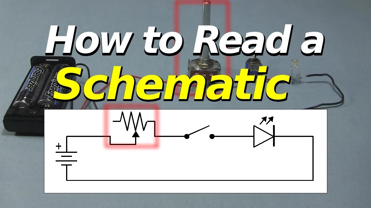
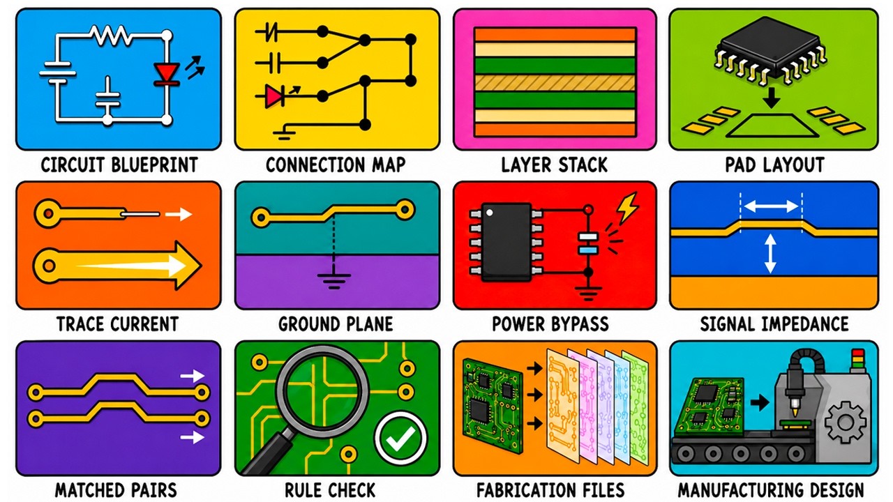

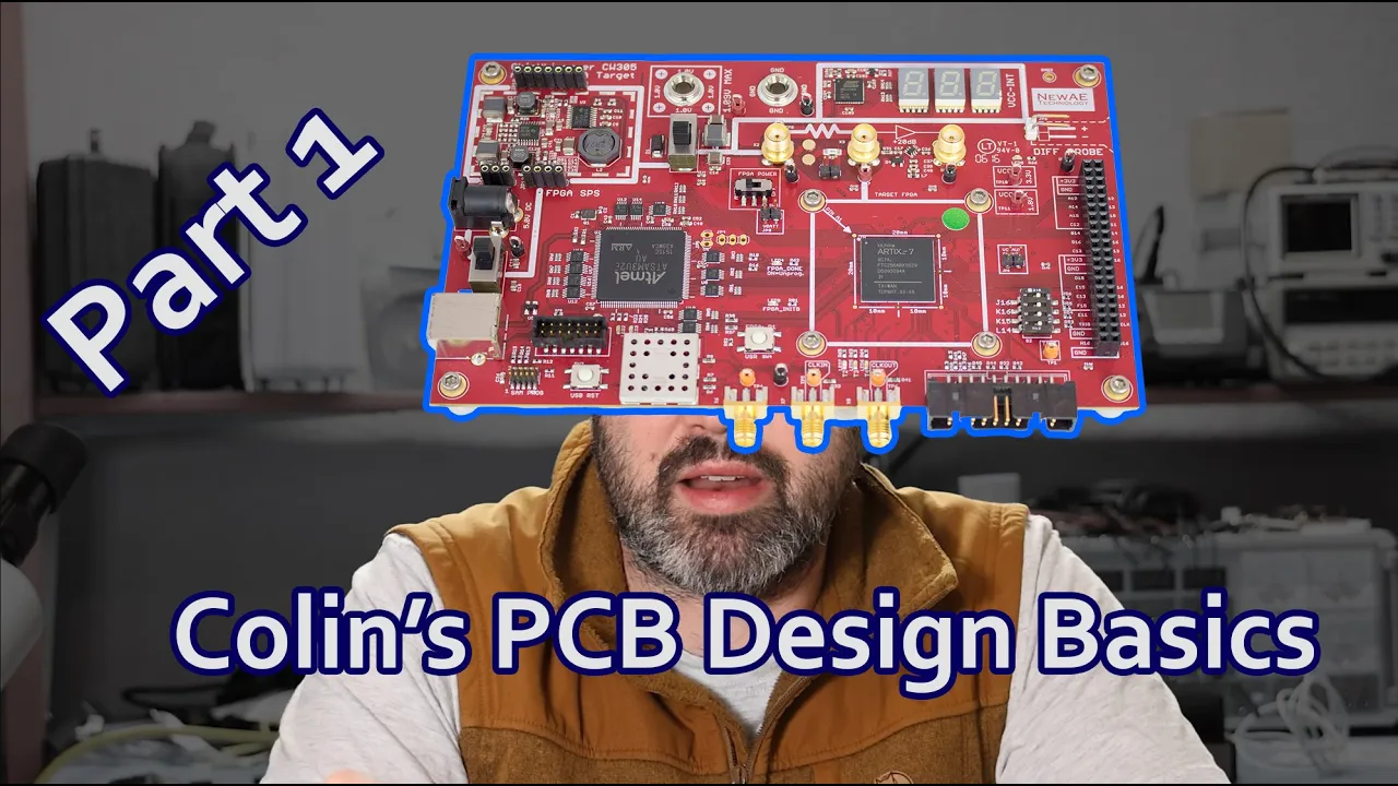
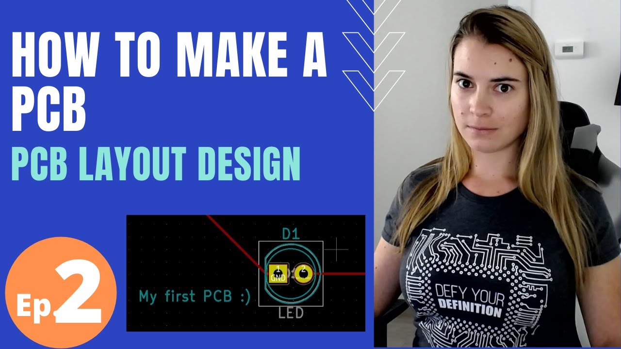

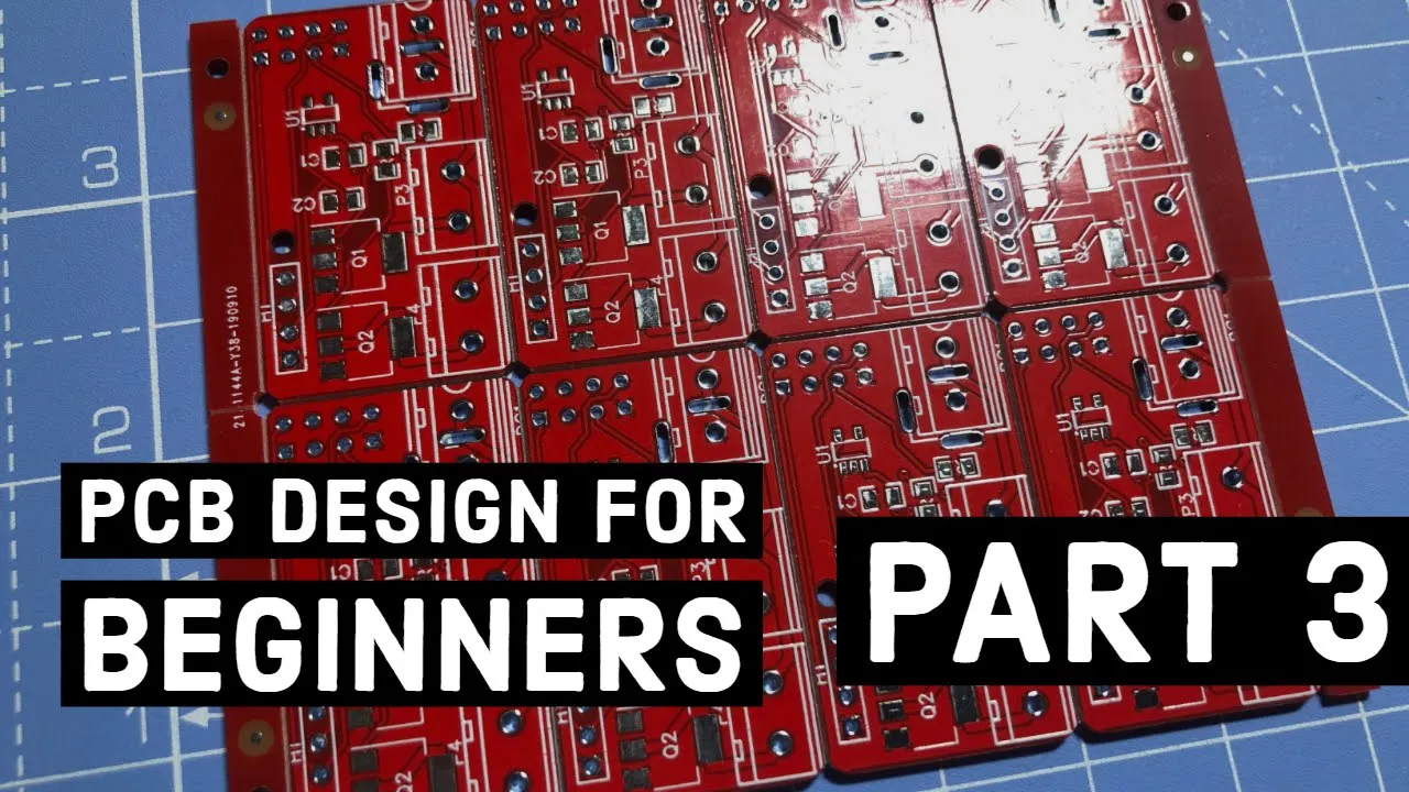










This tutorial demonstrates the complete process of designing a 5V regulated power supply PCB using KiCad software, covering schematic design with components like screw terminals, bridge rectifiers (DB107), electrolytic capacitors, and voltage regulators (LM7805), followed by PCB layout including component placement, routing, design rule checks, and Gerber file generation for fabrication.
Designing a 5V Regulated Power Supply PCB: KiCad Tutorial
Added:Understanding of basic electronic components, specifically linear voltage regulators (e.g., LM7805), decoupling capacitors, and diodes.
Fundamental concepts of DC voltage regulation, AC-to-DC conversion, and the importance of filtering ripples.
Basic familiarity with reading electronic schematics and translating schematic symbols into physical components.
Core concepts of printed circuit board (PCB) design, such as traces, clearances, and the distinction between schematic symbols and physical footprints.
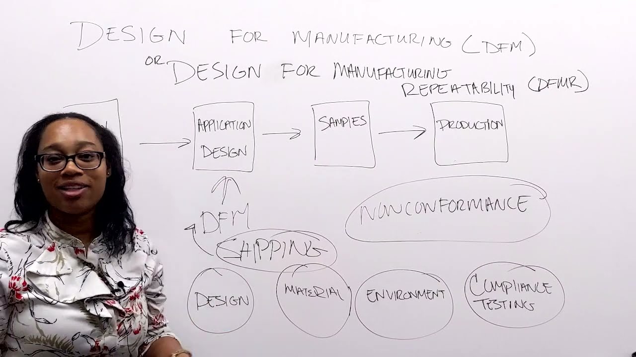
Design for Manufacturability (DFM) principles, including generating and verifying Bill of Materials (BOM) and panelization.
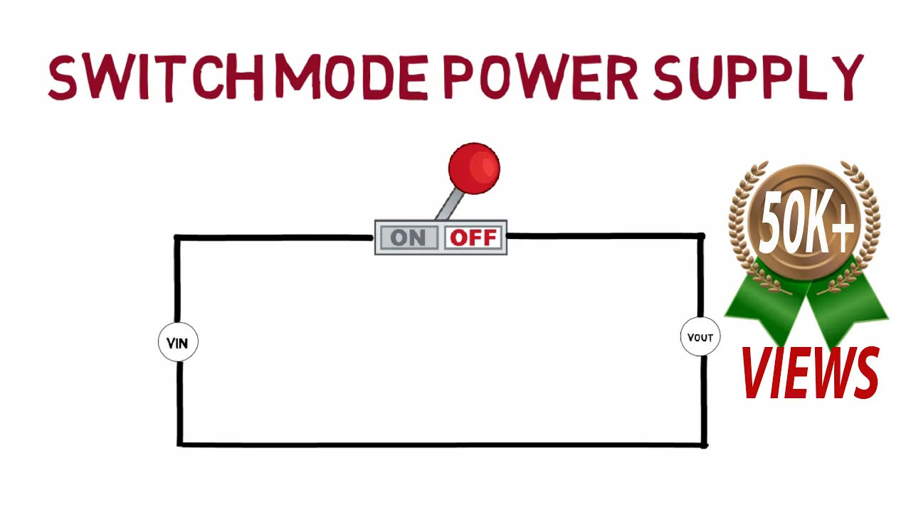
Advanced power supply topologies, such as high-efficiency Switch-Mode Power Supplies (SMPS) like buck and boost converters.
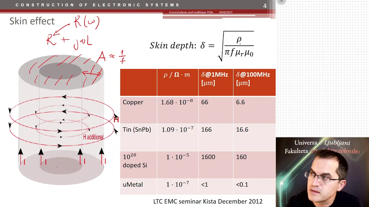
Multi-layer PCB design techniques, incorporating dedicated ground and power planes to improve signal integrity and reduce electromagnetic interference (EMI).
Thermal management strategies in PCB design, including calculating trace widths for current capacity, thermal vias, and heatsink selection.
7.6K views138likes41:22Original Release: 2024-03-26
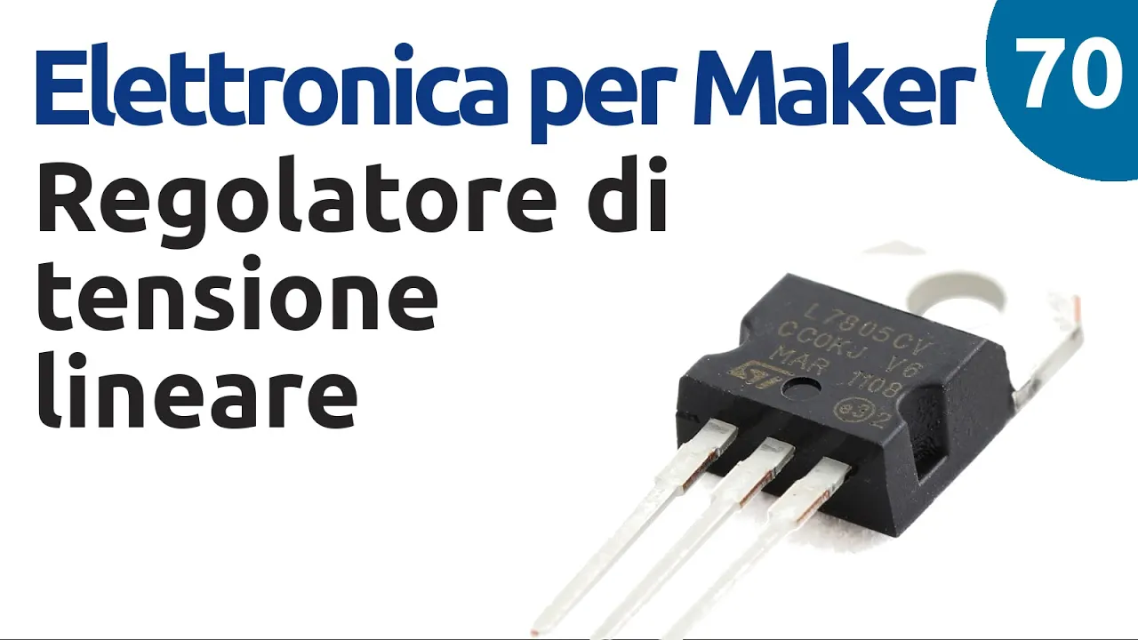
in this video we will see how to do a PCB design for uh AC to DC converter or uh um a mobile charger or 5vt regulated output DC output so in this circuit I'm going to uh open the sematic first before starting the PCP design we need to have an idea how this uh output should be like or uh what is your fabrication after fabrication how you are going to connect with the external world so in this uh video I'm going to consider the Step Down Transformer is outside of the PCP like I'm going to take the secondary side of the trans former output will be connected to a connector or a screw terminal into the board so in this PCB board we will have a screw terminal at input side and output side only we are going to focus on the converter part in this PCB so uh we need to take the components as per this uh configuration so I'm going to take uh screw terminal so in this um sematic circuit app we need to select the components what we need to what have in the circuit so just click on this add symbol you can see the third option here uh opam type of symbol is here otherwise the shortcut is you can press uh letter A in the keypad you will get that component list so first time while uh opening this choose SYM symbol it will take some time to load or to install the symbols uh because I already opened it immediately I I I saw this window but for first time it will take some time don't get confused with that and here you can uh able to get the component whatever we need by default few components are there in the key uh key key CAD suppose if uh symbols are not available or what you want what you want to connect in the circuit if the component is not available in the uh key CAD you can download and import the uh symbol uh footprint as well as 3D model one more video I will make how to import the symbol and uh footprint into the KE uh K can later I'll give the link in the description now first point is I'm going to import um the screw terminal so you can type screw so in screw terminal we have lot of options uh but I'm going to take two terminal one uh screw terminal 1 into two because um it is sufficient for me to take face and neutral of secondary side of the Transformer so you can choose this screw terminal 1 cross 2 after choosing this uh here you can see U my mouse pointer the symbol is uh in the top part of this uh choose symbol you can see the symbol of uh the screw terminal 1 cross two like that we have many screw terminals right but uh right now I need only one cross two after selecting the symbol I want to select the footprint also so after that you you need to click the drop down below this uh symbol sematic symbol you you have a drop down here here you can find your appropriate uh footprint for uh your screw terminal right so I'm going to search uh my screw terminal usually I will go for this ponic ponix 1 cross two horizontal if it is not suitable or if it is not okay with you you can come back and again change your footprint it is okay because we cannot memorize every uh What uh Footprints because they are more Footprints are there right so you can choose initially I'm going to choose this horizontal let's see how the terminal is I think this is a good for me the yellow color is nothing but the Sol ring mask which will be there by seeing this soling mod itself you can understand whether it is a through old or SMD through old uh will have this yellow color type of solder mask whereas if you see smds I think in to screw terminal there is no SMD I will show SMD in next another component so I think this is good for uh me to select this footprint and then click okay and then after click this you can see my mouse is following this I mean the symbol is following my mouse so it means that I need to place it somewhere in this canvas or working area of the sematic so I'm going to place this here right and still you can see my mouse pointer see you can see my mouse pointer uh some opam symbol is following in my mouse pointer it means that but means that still um uh my still my uh I have selected this component mode only so we need to press Escape if you want to do some other operation or if you want to still continue to add the component to the circuit you can still have the same and uh if you click with this symbol you can you can see that again it's going to the searching of the symbol so you can um what erase it if you don't want this by or you can remove this component selection option by just pressing the Escape it will it will move or or it will remove and I need one more screw screw terminal at the output side so I'm going to take one more screwdriver screw terminal the problem is here suppose if you copy and paste the same thing in second time uh it will not uh take the what footprint or it will not select the footprint only symbol will be copied so best practice is always go to the symbol selection and then take uh one more time this one because it uh by selecting the component one more time from the choose symbol it will enable the or it will merge the this symbol again I mean to your symbol where's this footprint to your symbol and I'm going to just rotate this by pressing um button R keypad R and I keep here and then I'm pressing escape to remove this component selection option from my mouse and you can see this uh the symbol name is here is J1 and then name of the symbol is crew Terminal 1 cross two here it is J2 and again the name of the symbol is crew terminal itself right now I want to take the bridge rectifier or you can take some normal diode itself and make a bridge but I want to select this bridge rectifier configuration using some uh IC so let's see I already selected some IC a bridge rectifier in that DB 170 is a bridge rectifier where we can uh take it directly to the circuit and it can give the supply uh rectifier output up to 1 amp load we can connect with this IC so I'm going to choose this um IC for my bridge rectifier application so let take the name name of the I is db107 so I'm going to search the db107 in the component so I'm going to type DB 1 07 here um and you can see after clicking this there is a symbol as well as um footprint is available for this db107 so we can take this suppose if you not find this symbol in your software you can see uh my one more video in that I have explained you how to import this uh uh uh what import a symbol and uh footprint and 3D moduel from uh external from other platform to this key CAD can click okay this and then I got this symbol here and I need a capacitor so I'm going to use the electrc capacitor so again click the component and then uh search for the capacitor so in this capacitor we I I choose this polarized capacitor because I need to use the electrolytic U capacitor and then you choose the footprint what type of uh capacitor you need so you can see in this drop down of this footprint there are few SMD in this SMD you can see the footprint is in red color it shows that the um uh copper on the top so it is uh it is SMD we don't want M we need through holes because we are we are going to only focus on the through hole and here I'm going to use uh I can see few more drop downs and then after all these SMD is over we can see a capacitor with through hold and uh I will take the first option from the through hold I'm going to select this scre hole that is 10 mm um length and uh 4.5 mm diameter and then 15 mm P I'm going to select this but you can see this this capacitor is um what um not in the horizontal uh that we we will usually keep the capacitor I'm going to change and see with the other model radial model yeah this one is fine so the radial model usually we'll put it is um we will take the capacitor in the radial model so we'll take the radial model with at least uh 6 mm diameter and then click okay and keep it for the input side and as well as the output side we need one more so I'm going to take one more capacitor and already it is selected so I'm going to just click okay and then past is paste this in the output side so just I'm planning there will be a screw terminal screw terminal in the input side where the the volage from step down side of the Transformer is feeded here and then before rectification I'm going to filter this and after rectification I'm going to filter again and then I'm going to give it to the screw terminal so this is what the plan is and we will take a voltage uh rectifier circuit so I'm going to take 7809 sorry 7805 7805 voltage regulator we will take and then I'll choose through hold horizontal so this looks fine so vertical I have chosen and then click okay so I'll keep uh here and then this is for the input capacitor and then this is for the output capacitor and then this is output terminal so that's it so we got all the component what we need for this circuit just we are going to connect this and always I will keep uh the one for pace and two for neutral if this is AC and one for VCC and two for ground if it is DC so you can um uh you can have your own way of connecting it until otherwise if you you are confident that your connections are proper you can have a clear idea right I'm going to just uh connect the components and then this one is the primary side of the Transformer is going to give uh in the pin number three and then this four pin can be connected in the Neal of this Transformer which is Con going to be connected in the terminal two of the J screw terminal one and then this plus I'm going to connect in the input side of LM 7805 this is the voltage regulator the output of this Vol Vol voltage regulator will give 5 volt always then I'm going to connect this negative to Terminal 2 and then this one to the output and this capacitor input capacitor I'm going to connect this this to here and then this to here and here to here so that's it our circuit is done here you can see circuit is done for a normal Bridge rectifier very small I mean circuit we have one Bridge rectifier which is db107 and we have two uh screw Terminals and one the first one is connected uh to the will be connected to the this uh secondary side of the Transformer and then screw terminal 2 is going to connect at the output side so at Junction screw terminal two we will get the output 5 volt always because we have connected the voltage regulator so we'll get the the 5 volt always 5 Vol at The Junction to this is the plan so we are going to make this um circuit so once this Matic is done then we can go for the PCB designing so for that you need to click on this tool and then press this update PCB for the sematic or the shortcut shortcut is um function pin a or f8 function pin 8 f8 and it will take some time to configure your asmatic into the PCB mode and it will it will direct us to the PCB and it will show if some I mean something is missing it will show the error here so we got two errors let me try to rectify the errors later and then if now for time being you update the PCB and then close it and if you see after completing this in my mouse pointer is carried I mean when I change the mouse pointer the components which I have uh taken from the sematic is carried out so you can place it somewhere so I'm going to just place it here for the time being and then if you zoom in and if you see we got the components right so we got the component here and let try try to let uh we check what is the error we are getting so once again I'm going to click on this uh tool and then update so the error is from C2 and J2 no footprint is assigned let me check what is that error go to this maatic and then this is C2 so this C2 and J2 C2 and J2 is not assigned the footprint so let me check this so click on this C2 click on this C2 then you can see um if initially we assigned the footprint directly from selection selection of the component but here because it is not assigned properly so we need to assign it again so click this double after double click go to this footprint and then uh click this three lines browse button where we can select the footprints for our needed so I'm going to check again capacitor cap capacitor capacitor electroly smds are there I'm going to take Electro SMD we need trim type of capacitor CP radial we will take at least 6 cm so now we got the footprint CP radial Dimension 6.3 and P 2.50 this is purely based on what type of capacitor you're going to use based on your size and uh things you can always refer your data sheet what is the diameter and then size uh strip size everything you can check it from the data sheet and based on the size you can select what type of capacitor or resistor you need and its respective Footprints then click okay so now footprint is assigned for C2 let's check once again what is the problem me any errors we are getting and go to tool and update the PCB you can see the error for capacity is removed and only error for the J2 is present and click on the update PCB and then close and after after completing the I mean assigning the footprint you can see my mouse point is carried out only the capacitor because the footprint footprint is assigned just now so um after completing or updating our PCB to the simatic from simatic to PCB this capacitor alone coming with my m pointer so you can place it somewhere here and then let me check for the junction two also that is screw terminal double click it again and go to the footprint and choose the footprint what we need for this Junction So to avoid this error we need to uh second time what happened is when I choose the component I have assumed that the footprint is visible so it is selected but it is not actually selected even though the footprint is visible so what we need to do is we need to click on the footprint uh in the drop down also in the initial stage of selecting the component so again here I'm going to type screw terminal so screw terminal we need two right so I have I'm choosing the first option terminal block you can see the two pin terminal pitch 5.0 mm so this is okay for me so I'm just going to click this and uh click okay so now footprint for the terminal 2 also assigned and then I'm going to just click the okay let's check the errors there is no error and you can see this the mouse PO is carrying carry out the footprint of this one and you can see the terminal 2 footprint I have chosen different and terminal one is different so it is appropriate to take what type of footprint you need um and you can see this there is no big different in actual holds uh by seeing this the holes are okay but still the outer layer and the size are maybe differ but as long as you get two holes to connect your terminal it is okay but if you need a proper design or proper way of connecting the terminal refer your data sheet and based on your data sheet we need to choose our terminal so J1 is the input and J2 is output in this case and now next immediate thing is we need to uh arrange the board arrange the circuit as compact as possible uh to see our uh uh to exactly get the PCB board as compact as possible because the size of PCB uh is uh uh directly proportional to the cost also so if you have a bigger size of PCB then cost is also going to be higher production cost will be higher so always uh even um customers need the smaller size instead of bigger one so we need to we always try to minimize the size and uh so because uh to minimize the size we need to have a clear idea about how we are going to design this so just we have a 3D view uh in this moment I not connected anything so you can see in this three 3D Junction two I don't have 3D because uh I have chosen the footprint later but injunction one have the 3D printer okay so what I'm going to do is I'm going to delete this J2 and then I'm going to again take the J2 to the sematic let's check how how I'm doing that so go to the schmatic and then just delete this because I don't want this I'm going to add Junction two from the actual footprint itself so type screw terminal on crust two and then select the appropriate uh so I'm going to take This ponix 1.2 horizontal with 5.8 mm right so click okay and then connect this so the ground I'm going to connect with ground I'm going to connect this this wire and then and then this is for the VCC so it is connected again go to this update maatic and then update this I'm going to delete this and go to PCP and update this so after updating I got the new screw terminal which is added recently so just click that now you can see 3D View so I got yeah again you can see this the size from one to another is different because this is 5.8 and this is five so uh it's okay for just for the simulation sake but if you're are taking the actual circuit we need to take the data sheet and then based on the data sheet you need to select what type of component you're going to take even though the symbol is okay but um the footprint is matters more so you need to take appropriate uh uh what components uh but if you're okay with this and um in actually you are taking um what you are going to buy the screw terminal in the equal size this 3D model is not that much important until otherwise the size of this Lids are fixed fixing together okay let uh we start to do the track part so I'm going to close this 3D view for now and then let me try to connect this if you see actually the screw is this side so we need to keep the screw outside of the PCB so I'm going to turn my uh terminal like this so that you can see the 3D view is turned like this so that uh the customer can screw their wire they can fix the wire in that so this corner is I'm taken so as a input and then I'm going to take this is same way I'm going to take this this side let's check but it is in the reverse side right so it is I'm expecting this SC or the wire should be inserted this side so I'm going to turn it again up 18 180° so let's Che yeah now it is fine so wi customer can put wire here and then they will tight the screw here so it looks fine right and then yeah let me take the bridge rectifier see there are some mild blue color line is given it shows us the how the connection based on our sematic so always uh make sure that you don't have more twisting in the track so I'm going to try I'm trying to minimize the twisting like this fine and then this is the voltage regulator I'm going to keep here and this is the output capacitor and this is the input capacitor and this is the outer screw terminal let we rotate this to minimize the twisting let me remove all this silk screen and then let me check I'm going I don't want to see this names and other things I'm going to just remove the S screen and then we can check this you can see so this line is going in the top so and this one it's connector here so try to rotate this but if you if I rotate this again there is a Twist so I'll take it back to the original position like this and then let it be so what we can do is we can bring this down so that it will eliminate all the problem okay so this is how we need to make a decision to minimize the size or uh to make as simple as possible so if we reduce or if you are okay or if you try to minimize the twisting here while placing the component it will eliminate or it will make easier to the connection right so after plac ing this then we can go for the outer cut outer cut is nothing but uh how we need to cut the PCB or the size of the PCB right so for that you you select this Edge cut you can see my mouse pointer so there is Edge cut here right you can select that edge cut and then click on this rectangle draw rectangle after that just go to any one corner uh that you want to make the circuit and then click there and then just drag it till how much you need so while dragging you can see the size of the board in X and Y AIS that is in X it is 65.9 6 mm and in y it is uh 20 m mm that is nothing but 6 cm to 2 cm size so that that much compact we can make this circuit right so I'll try to make it 66 and 21 okay nearly 21 I'm getting so I'll fix this yeah now um you can see go to view and then go to 3D view you can see this is the board I'm looking for uh for this bridg that is that is not 3D model because that components I have imported from third party so but still the footprints are proper if you buy in the local store and uh you can fix it in the board so it will work fine right so let me start the routing part I'm going to make this as a single layer so I want uh the lines to be in the back side of the board so I'm going to take the track in the back copper so click this second option that is the blue one I can zoom and show you this is the second this is the front copper this is the back copper so I'm going to select this back copper I'm going to uh select the route track so click this first you select the back copper and then select this routing and then and then yeah Zoom it by scrolling your wheel Mouse wheel so I recommend you to use Mouse even though if you're using the laptop because uh Mouse will make you uh the connection easier because many times we need to zoom in and zoom out so better to use the mouse and then um the scroll because it is needed so I have selected as I said I have selected the back oper and then track and just go to the line where you need to connect so this lines the blue mild blue lines will guide you how to connect route the PCB and just drag and drop this so once I click here it it will highlight where should be the next connection based on our sematic so the immediate one always I will click here I will connect here and then from here it is this and then from here it is this and then from here this and then from here to this this to this okay but I feel the ground should be connected in the ground but uh let's check the connection if the connection is wrong again we can revisit yes I missed uh here you can see I missed the ground should be grounded here that part is missed so I'm going to connect that then so make sure that the circuit is proper otherwise uh the sematic will not show your connections because this uh Kad is not the actual simulator is just follow what we have connected so make sure that you have a appropriate circuit with you and then connect based on that so now I'm going to update this and then close see after updating I can see one more line is added in this ground so yeah now we'll we will connect this again select this routing and then connect this you can connect either here or here anywhere is okay but I'm going to connect here okay fine so now the connection is done and uh yeah so this is very simple circuit I have connected let's see the 3D view of this so in top side there is no any tracks and in the bottom side you can see the tracks right so this is how the circut is done so now our normal Bridge rectifier is ready okay uh in upcoming videos we will see how to add some S screen add your name some meaningful names like ground BCC those things we'll see in next video this video is just to understand the basic working of PCB Kad design I mean PCB design using Kat right so important things is we have three area one is sematic in that sematic you need to choose your component for your circuit and you need to connect the circuit properly and you need to choose appropriate uh uh footprints for each and every component once it is done and uh make sure that the routing is proper and the placement of the routing is also important to reduce the size and uh finally you can go and check your U 3D last but not the least there is uh design rule check we need to confirm our uh What uh the connections are proper so for that you can go and uh check your uh design and click this design rule check and then run DRC and we got zero error and zero warning uh but if the circuit is going more complicated and complicated we we can we may miss some part like uh the gap between two tracks and then overlapping uh and those errors can be uh bring B bed out to our knowledge from this design rule check okay so it is very important to make this design rule check and then close it and finally we need to uh send this to the factory right so without sending to the factory we cannot fabricate this so Factory need a few files like um friend copper back copper drill and all other I mean silk screen right cut layer okay all these things can be made in One Click by just click on the file and then go to fabrication output and click on this gber file gber and then uh before generating the gber you can generate the drill files so click on this drill files here you can here you can choose what of the files need to be uh sent to the factory So like um uh this is the front copper back copper and uh uh I don't want all these things I want very important things like front Sil screen back S screen front mask and back mask hedge cut these are all the very important things I'm going to uh send all these things to the fabrication so for that I need to plot the goo file right so before that we can choose where the go file need to be stored so as I already opened opened a folder new folder called charging circuit which is shown in the first video of this series here I'm going to choose a folder called gber so I'm going to select this folder to what generate the goo file here you want to use this path yes can click this yes and then generate the drill file first and then generate the drill files and then close it and then plot so once uh plot is done you can see the goo file these are all the gper file generated right copper back copper back S screen Edge cut all these things are the fabrication files that we can send into the uh PCB fabrication unit uh just by making this to the zip file so we need to add it to the zib so so this ZIP file we can send uh to any of your PCB fabrication unit they will make the PCB what you have designed and then they will send the PCB to you so finally PCB the fabricated PCB will look like this and uh in the fabrication they will not assemble the component until you you ask for it uh by default they will give only the board some Feb fabricator they can do the assemble service also for that they will charge extra cost otherwise you can buy and uh do solving by yourself right so that's all from the first video thanks for watching this video and uh please follow my YouTube channel subscribe my channel to get uh other uh technical tutorial videos timely thanks
Up Next
49:56
KiCad PCB Design: Schematic to Gerber Workflow Guide
@shabaz_
91.7K views•2022-01-17
12:54
Triumph of Orthodoxy Icon: Byzantine Art & History Explained
@BenCallan
2.1K views•2024-08-06

9:49
FastAPI vs Flask vs Django: Choosing the Right Python Web Framework
@TechWithTim
302.5K views•2024-05-26

1:42
Game of Thrones Opening Credits: A Cinematic Analysis
@gameofthrones
46.3M views•2011-04-18
Related Study Plans & Knowledge Roadmaps
Structured learning paths in General & Interdisciplinary Studies
general-studies
Elevator Engineering: History, Physics & Cities
01From Hoists to Safety Brakes: The Dawn of Vertical Lift
02Hydraulic vs. Traction: The Engineering Physics of Elevators
03Modern Speed, Safety, and Algorithms
+ 2 more learning modules
12h5 modules
Explore Roadmap
general-studies
Rubber: Material Science, History & Geopolitics
01Origins of Natural Rubber & Mesoamerican History
02The Chemistry of Natural Rubber & Vulcanization
03The Geopolitics of the Rubber Boom & Colonization
+ 2 more learning modules
12h5 modules
Explore Roadmap
general-studies
Containerization: Evolution, Logistics & Trade
01Ancient Trade & Bulk Cargo: Amphorae to Barrels
02The Industrial Revolution & Cardboard Packaging
03The Containerization Revolution: Malcom McLean
+ 2 more learning modules
12h5 modules
Explore Roadmap
general-studies
Textile Tech: Evolution, Labor & Global Impact
01Pre-Industrial Textiles: Handloom & Cottage Industry
02Mechanization: The Spinning Jenny to the Power Loom
03The Factory System & Global Labor Transformation
+ 2 more learning modules
10h5 modules
Explore Roadmap