


















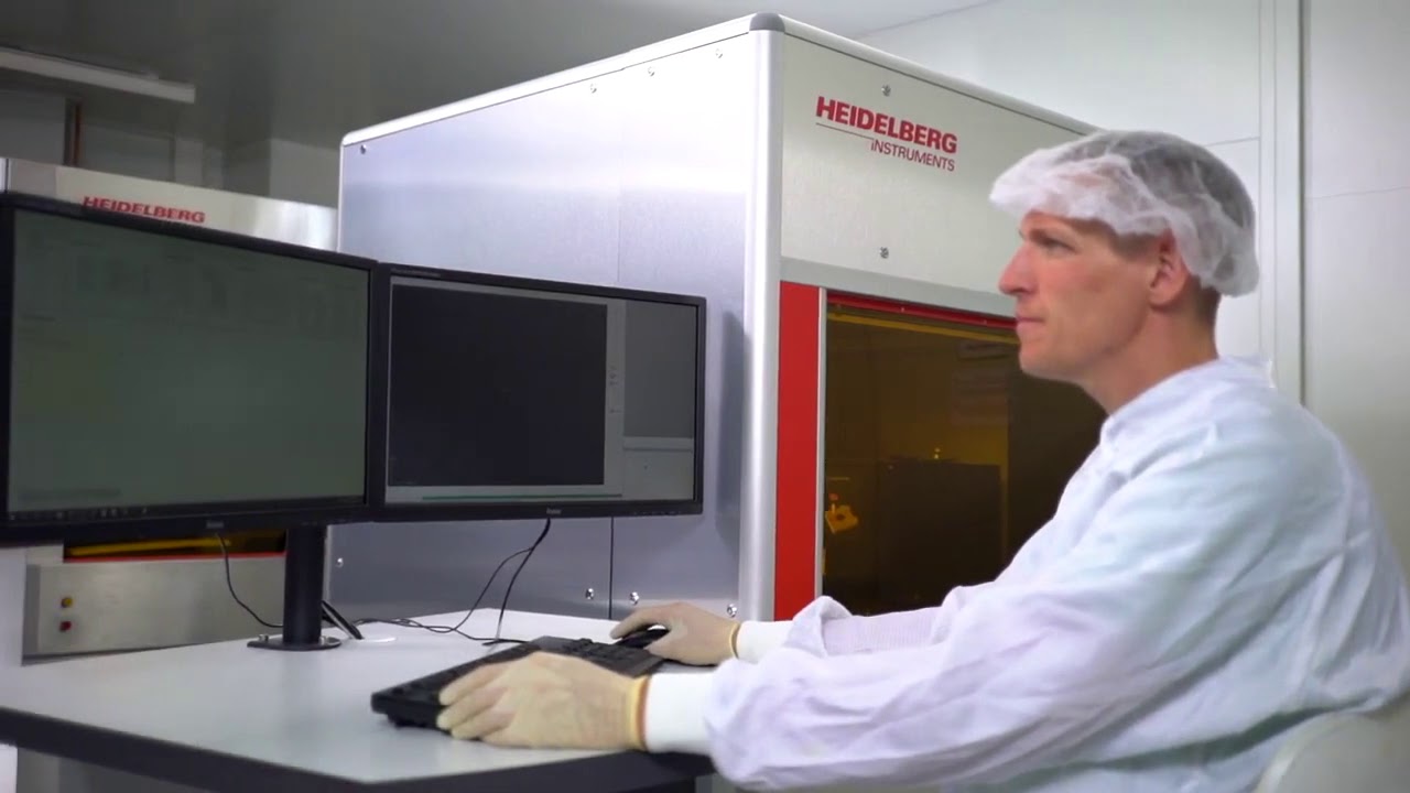


This video demonstrates the complete SU-8 photolithography workflow for creating microstructures: wafer cleaning with acetone and IPA, spin coating SU-8 2035 at specified speeds and times, soft baking, mask alignment with water contact layer, UV exposure with calculated dose, post-exposure bake, and development in SU-8 developer with IPA rinse. Key parameters include spin speeds of 500 rpm (15 sec) and 3,000 rpm (38 sec) for 35-micron layers, soft bake at 65°C (2 min) and 95°C (5 min), and post-exposure bake at 65°C (1 min) and 95°C (6 min).
Photolithography: SU-8 2035 Soft Lithography Process (UC Berkeley BNC)
Added:Basic Photolithography Principles: Understanding the standard sequence of wafer preparation, spin coating, exposure, and development.
Negative vs. Positive Photoresists: Knowing that SU-8 is a negative photoresist where UV-exposed regions become cross-linked and insoluble in the developer.
Role of Photomasks: Understanding how UV light patterns are transferred onto a substrate using a photomask, specifically comparing Mylar film masks to traditional chrome-on-glass masks.
Cleanroom Safety and Chemistry: Awareness of cleanroom protocols and safe handling of microfabrication chemicals, including SU-8 resist, developers (like PGMEA), and isopropyl alcohol.
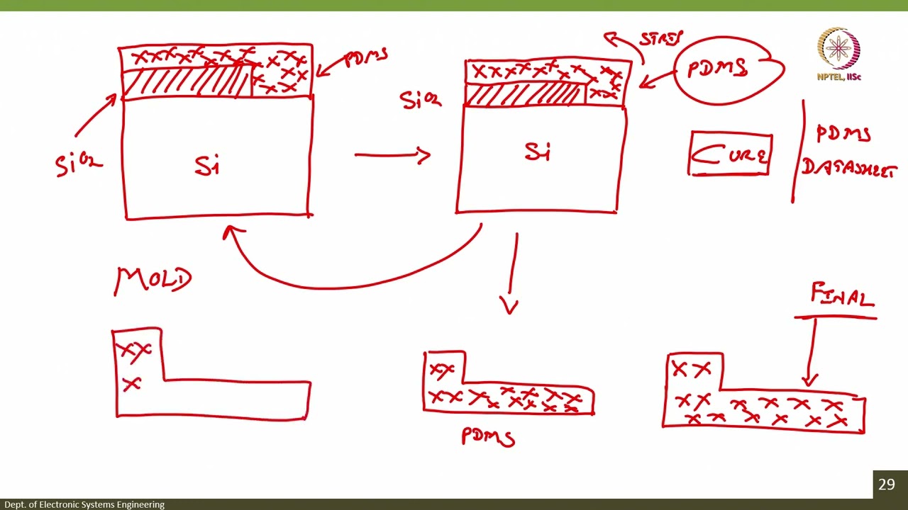
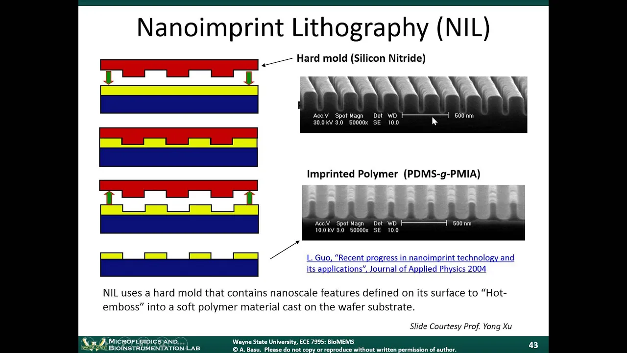
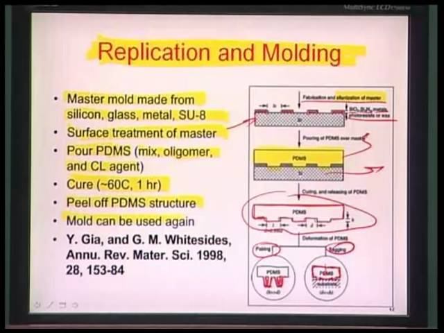
PDMS Casting and Replication: Learning how to use the fabricated SU-8 structure as a mold (master) to cast polydimethylsiloxane (PDMS) for elastomeric microfluidic devices.
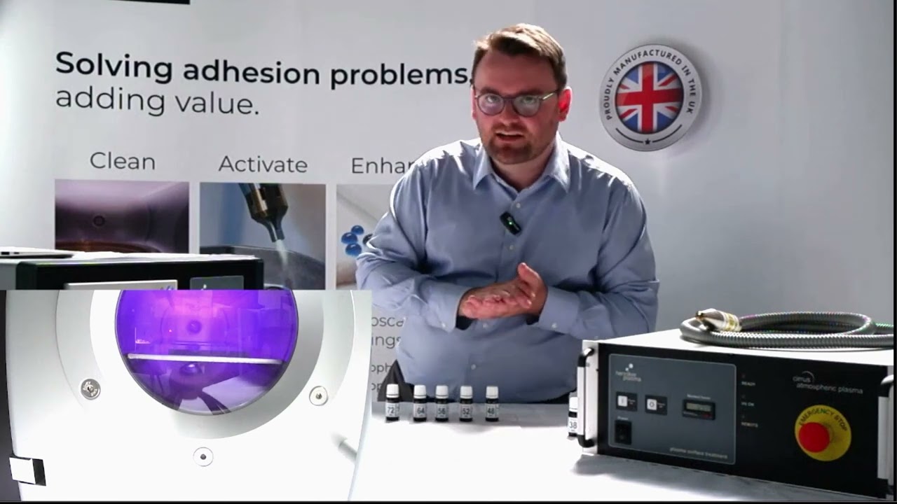
Oxygen Plasma Bonding: Exploring how to permanently bond PDMS channels to glass substrates using oxygen plasma treatment to seal the microfluidic devices.
Metrology and Quality Control: Utilizing tools like optical profilometry or Scanning Electron Microscopy (SEM) to measure the height, sidewall angle, and resolution of the cured SU-8 features.
Multilayer Lithography: Developing advanced techniques for spin-coating and exposing multiple layers of SU-8 to create complex, multi-tiered 3D microstructures.
Microfluidic and Lab-on-a-Chip Applications: Studying how the finished chips are integrated into biomedical, chemical, and physical analysis setups (e.g., cell sorting, droplet generation).
7.7K views26likes10:36Original Release: 2014-02-18
[MUSIC PLAYING] INSTRUCTOR 1: This is a basic walkthrough for soft photolithography in the BNC.
The first thing that you want to do is turn on the vacuum in 146A, which is the room next to the clean room.
And this is the vacuum for the aligner and one of the spinners.
Before you turn on the lamp, check the log sheet.
And make sure no one has signed out within the past 30 minutes.
And then turn on the lamp for the aligner.
Flick the power switch and hold down Start until it gives you a voltage and intensity reading.
If you don't get a reading, turn the power switch off and then on again, and then hold down Start.
Before you can use the lamp to expose, you need to give it 30 minutes to warm up.
Fill out what time you turned on the lamp in the log sheet.
INSTRUCTOR 2: The readings on all of our hot plates are wrong, so double-check with the infrared thermometer.
You need to set three hot plates-- one to 65, one to 95, and one to 120 degrees Celsius.
Now you'll need to clean your wafer.
Start with acetone, which is in the red top bottle.
Make sure to thoroughly rinse your wafer, and then an IPA rinse.
IPA is in the yellow-top bottle.
Next, do a water rinse.
And then air-gun the wafer dry.
Then place your wafer on a 120-degree hot plate to dehydrate.
And cover with a glass container to prevent dust.
If you use the spinner across from the aligner, you need to turn on its own vacuum as well.
INSTRUCTOR 1: Now you can turn on this spinner and program your spin cycle.
So first, you press Program, then you enter what program number you're going to call this.
Confirm that dispense is off by pressing Enter.
These are the parameters for spinning a 35-micron layer with SU-8 2035.
First speed, 500.
Ramp speed, 100.
Total time, 15 seconds.
Second spin speed, 3,000.
Ramp speed, 300.
Total time, 38 seconds.
Load the wafer onto the chuck.
You can use the aligning bars to help center the wafer.
INSTRUCTOR 2: To run the program, press Run and select the number we titled our program.
Press Start, and it will test the centering.
If the wafer isn't centered, adjust the wafer.
Press 0 to retest.
When your wafer is centered, pour on your SU-8.
Keep the lid of the bottle close to the wafer and pour in a continuous stream to avoid bubbles.
You should cover about 60% of the area of the wafer.
Close the lid and press Start to start spinning.
When it's done spinning, the spinner will beep.
And you can lift the wafer up from the chuck.
Now we're going to do an edge bead removal.
The simplest way to do an edge bead removal is to carefully use a cleanroom wipe to wipe the circumference.
Then, soft bake the wafer.
First, bake at 65 degrees for 2 minutes, and then 95 degrees for 5 minutes.
Then, take the wafer off and let it cool.
Then, using your tweezers, carefully test the edge of the SU-8 on the wafer to make sure it is no longer soft.
While you're letting it cool, half an hour should have passed.
So you can turn on the aligner.
First, we need to test the energy level of the lamps for the day.
So take the photometer and place the sensor blue side up on the stage.
And then set the exposed time to 2 seconds.
Turn on the photometer.
And pull the stage over to expose.
And keep your eye on the photometer and record the highest reading and outputs.
Record that in the logbook.
INSTRUCTOR 1: Then load your mask in by unscrewing the mask holder.
Be careful not to kink the hose when you turn it over.
Unscrew the black screws.
And be sure not to drop the screws into the machine.
Air-gun your mask.
Use a razor blade to test which side is the ink side on your mask.
The razor blade should scratch off on the ink side, as you can see here.
Use a small pipette to get some distilled water.
Place one droplet onto the center of the clean glass on the stage.
Place the mask ink side up, mylar touching the glass, and then use a dry cleanroom wipe to spread the water into an even layer between the wafer and the glass.
Avoid leaving bubbles.
You'll be able to visibly distinguish where there is and isn't water.
INSTRUCTOR 2: Replace the black screws and the mask holder and screw it in place.
Push the switch in for the mask vacuum.
Open the stage and load in your soft baked wafer with the flat side facing you.
And align it to the small metal nubs on the back of the chuck.
Close the stage and make sure that the ball vacuum is unlocked.
Then, turn on the substrate vacuum.
Adjust your y and x-axis knobs to center the chalk underneath your mask.
When it is all centered, use the z-axis to bring the wafer up.
Do not overturn the Z knob.
Watch contact occur as the wafer approaches the mask.
You'll be able to feel when you have turned the z-axis to the maximum.
INSTRUCTOR 1: After it's in contact, turn on the contact vacuum.
Set the exposure time, which you can calculate using the formula on the screen.
Again, tell everyone to look away when you expose.
And pull the stage over to the lamp.
You'll hear when the exposing starts and stops.
When you're done exposing, bring the stage back over.
Turn off the contact vacuum and lock the ball vacuum.
Use the z-axis to bring the chuck down away from the mask.
The wafer should not stick to your mask.
If it does, you did not soft bake for long enough.
Open up the stage.
Turn off the substrate vacuum and remove your wafer.
INSTRUCTOR 2: You should not be able to see any features on the wafer.
If you do, that means you overexposed.
Take it over to the hot plates for a postexposure bake, 1 minute at 65 degrees and 6 minutes at 95 degrees.
As it bakes, you will see the features appear.
Take the wafer off the hot plate and let it cool.
You should see your features.
INSTRUCTOR 1: Pour some SU-8 developer into a clean container.
Submerge your wafer into the SU-8 developer once it cools.
You can manually swirl the dish.
Place it on the shaker, or use a bottle of SU-8 and spray it down.
Your total developing time will probably be around 1 minute.
When it looks like there is no residual SU-8, spray some IPA on it.
If a white residue forms, it is not done developing.
So continue developing, and spray it down with the SU-8 developer.
If the rinse is clear, then spray down the entire wafer with IPA.
Rinse with water.
And air-gun it dry.
You may do an optional hard bake at above 120 degrees for 5 to 30 minutes.
[MUSIC PLAYING]
Up Next

16:19
Organ-on-a-Chip Technology: Engineering Human Organs | Dan Huh | TEDxPenn
@TEDx
57.4K views•2015-06-09

12:54
Triumph of Orthodoxy Icon: Byzantine Art & History Explained
@BenCallan
2.1K views•2024-08-06

9:49
FastAPI vs Flask vs Django: Choosing the Right Python Web Framework
@TechWithTim
302.5K views•2024-05-26

1:42
Game of Thrones Opening Credits: A Cinematic Analysis
@gameofthrones
46.3M views•2011-04-18
Related Study Plans & Knowledge Roadmaps
Structured learning paths in General & Interdisciplinary Studies
general-studies
Elevator Engineering: History, Physics & Cities
01From Hoists to Safety Brakes: The Dawn of Vertical Lift
02Hydraulic vs. Traction: The Engineering Physics of Elevators
03Modern Speed, Safety, and Algorithms
+ 2 more learning modules
12h5 modules
Explore Roadmap
general-studies
Rubber: Material Science, History & Geopolitics
01Origins of Natural Rubber & Mesoamerican History
02The Chemistry of Natural Rubber & Vulcanization
03The Geopolitics of the Rubber Boom & Colonization
+ 2 more learning modules
12h5 modules
Explore Roadmap
general-studies
Containerization: Evolution, Logistics & Trade
01Ancient Trade & Bulk Cargo: Amphorae to Barrels
02The Industrial Revolution & Cardboard Packaging
03The Containerization Revolution: Malcom McLean
+ 2 more learning modules
12h5 modules
Explore Roadmap
general-studies
Textile Tech: Evolution, Labor & Global Impact
01Pre-Industrial Textiles: Handloom & Cottage Industry
02Mechanization: The Spinning Jenny to the Power Loom
03The Factory System & Global Labor Transformation
+ 2 more learning modules
10h5 modules
Explore Roadmap