


















Multilayer soft lithography is a microfabrication technique for creating multi-layer microfluidic devices, involving sequential steps: (1) Mold-making using photolithography with negative resist (SU-8) for control layers and positive resist (SPR) for flow layers, where resist thickness determines channel height; (2) PDMS replica fabrication by mixing base polymer with cross-linker (5:1 ratio for control layers, 20:1 for thin layers), degassing to remove bubbles, and baking; (3) Layer bonding through thermal annealing at 80°C where cross-linker diffusion creates permanent bonds between layers; (4) Final glass-PDMS bonding using oxygen plasma treatment. This technique enables precise control over microfluidic channel dimensions and complex device architectures.
Multilayer Soft Lithography for Microfluidic Devices | Stanford Foundry
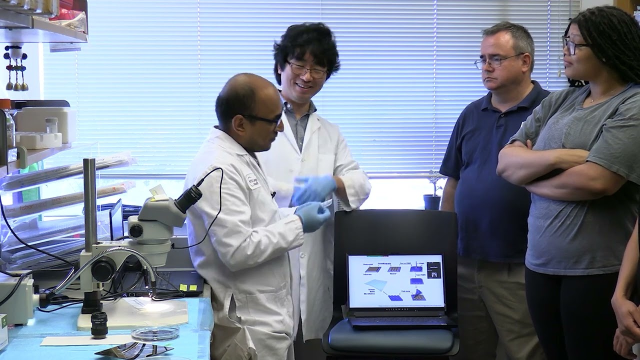
Added:hello my name is Michael instead I'm going to show you how to make a rotor function using more to airsoft demography brewery function is one of our simple devices the first step in multi-layer soft lithography is mold-making since the rotary pump chip is a multi-layer device requires two moles one mold control layer and one mole slowly the control mold is made using native resist which has a rectangular cross section and the flow bulb is made using positive resist which has a rounded prospect and after reflow this router cross-section ensures complete sealing of the channels of the flow layer during operation of our concluded device the negative region is particularly used in su8 which can achieve thicknesses of 5 to 150 microns the positive regions we can who use is SPR we should achieve thicknesses of 545 microns this thickness is determined by the viscosity of resist and also the spin speed and iteration the thickness of the resist interval determines the channel height of your microfluidic device at first going to be making the control mold we use sq8 which is a negative photoresist when we do that we spin the photoresist under the Waker so after the sting is done we take the wafer and soft bake it in two steps one step 65 degrees and then at 95 degrees and then we expose it we expose the way for honor Karl says contact the letter let's try to TV light from a photo mask on the wafer we use two different type of photo masks one being a transparency vents the other big a chrome mask to transparency mask tachi resolutions of approximately 10 microns the chrome mask HG resolutions of below 1 micron but is significant or obsessive the transparency mask this is a negative tone mask for use with negative resist this is a positive tone mass creation closet resist after we load the mask we load the wafer and expose after exposing the wafer we do a two-step post exposure bake one step at 65 degrees one step at 95 degrees and then we let the way for cool before we develop after post exposure bake we develop the wafer since this is negative resist the developer removes any onyx would resist transferring the pattern for the mass part of the wafer as you can see after developing the pattern from the baskets transfer to the wafer wafer is now ready for Harvick for both the flow of control valve use for flavors there are some differences the steps for making the flow and control for the flow bowl before we put the way for exposed to an agent protocol agent is after the adhesion promoter we cooked away from after coating we do a single step some fake of the way after the soft bake we expose the wafer is a global we use positive resist and for positive resist we use it positive tone Matt's after the exposure we immediately develop the waiver in positive development the positive developer removes any photoresist that has been exposed to UV lights as you can see after validating cleaning the pattern from mask is transfer to the wafer now the wafer is ready for reflow and carpet once the mold of heart Bank we treat that with a solid ice agent we use either TCS or TM CS treatment with the solid agent makes the PDMS not stick to the mold and makes it easier to work with PDMS is a silicone elastomer that consists of two components and a component and a big component the manufacturers recommendation for the mixing ratio is blended channel first when we making the PDMS for the control layer of the rotary pump we'll be mixing a five to one ratio of peanuts so we had a more two components your a and the beat so we take the mixed PDMS and pour on our wafer in this case this is our control way from as you can see there are plenty of bubbles in the PDMS if we were to make the chip right now the chip would be useless be full of bubbles so the next step is we D gas Leedy gassing takes about half an hour once the bubbles are removed we bake this layer for about an hour to partially cure it so then we can thoroughly bond it to the 120 layer for the flow layer for the Rotary Club we do a thin layer PMS and that's a 20 to 1 ratio and this is a similar spin coater that we used for the photoresist and then we spit it once the spinning is done we remove the wafer and bake it for approximately 40 minutes once the baking is done we remove our fuels you and peel it away from the whole that we individually cut out each ship more lazy once the hole is have been punched we clean the wafer to do that we use masking tape masking tape is great for moving any small particles of PDMS a dust that may have gotten on the wafer you place your thick layer on top of your thin layer trying to align with your alignment marks you that after we are aligned we then make the the chip at 80 degrees for another hour after incubating for an hour we take the chip out at this point the two layers should be bonded together because of the thermal bonding from the two different ratios the cross linker and the five to one ratio is diffusing over the interface between two layers into the twenty to one ratio so we should have a single piece of PDMS once we punch all the holes we put the chip and it clean glass slide into an oxygen pocket system we use this to bond the PDMS to the glass slide what this does is it modifies the surface of both the PDMS and the glass slide so we can bond them together it's a very strong permanent bond once this process is done we take out the chip in the slide and place the chip on our substrate and it bonds once we place it on we put this in the oven for another 10-15 minutes just to ensure we have a good bond after Plaza flooding we generally wait overnight to test the chip you can see this is a very strong bond I can't feel it off my fingers to test the chip we place a a 20 gauge needle into the hole connection to tygon tubing to an air source you can see on the screen this is the the rotary pump and it I turn on the on the air to turn the valve on that's closed that's open generally these work and around 10 psi this concludes our video of the production of a microfluidic device from the from the mold-making to the chip making if you have any questions please contact the Stanford micro fluidics tagger
Up Next
PDMS Bonding for Microfluidic Devices with Plasma Treatment
@harrickplasma942
6.6K views•2021-02-22
Ultrasonic Transducers: Resonant Frequency Measurement and Horn Design
@imajeenyus42
229.9K views•2017-02-22
Polymer Environmental Degradation: Mechanisms & Stabilization
@iit
1.8K views•2012-07-10
How a Student's Question Saved a NYC Skyscraper from Collapse
@veritasium
22.8M views•2025-04-26
Related Study Plans & Knowledge Roadmaps
Structured learning paths in Engineering