The mechanical exfoliation method, commonly known as the scotch tape technique, produces graphene by repeatedly peeling thin graphite flakes with adhesive tape until nearly transparent single-layer graphene regions form; these can then be transferred to silicon wafers and identified under optical microscopy as purple spots, with multi-layer graphene appearing at the center and single-layer graphene at the corners.
How to Make Graphene: Scotch Tape Method Tutorial
Added:Deep Dive
Understanding the atomic structure of carbon allotropes, specifically the structural difference between 3D graphite and 2D graphene.

2️⃣3️⃣ KARBONUN ALLOTROPLARI I GRAFİT I ELMAS I FULLEREN I GRAFEN I Asistanim Kimya
1.5K
Graphite is a three-dimensional carbon allotrope with layered structure held by weak van der Waals forces, making it black, shiny, and conductive. Graphene is a two-dimensional single layer of graphite, transparent, stronger than steel, and highly conductive. The structural dimensionality difference creates dramatically different properties: graphite's layered structure allows sliding between layers, while graphene's single-layer structure provides exceptional strength and conductivity. This illustrates how atomic arrangement determines material properties.
Click to watch →

Class 9 Chemistry || Important short questions || chapter 1 new book || Exam 2026
213
Both graphite and graphene have a hexagonal layered structure of carbon atoms, but they differ in dimensionality: (1) Graphite is a three-dimensional layered structure where hexagonal rings repeat in multiple layers. It is used in pencils (mixed with clay) - more clay makes harder pencils, more graphite makes softer pencils. (2) Graphene is a two-dimensional single layer of carbon atoms arranged in a hexagonal pattern. It is used for developing flexible, lightweight touch screens. The key difference is that graphite has multiple layers (3D) while graphene has only one layer (2D).
Click to watch →
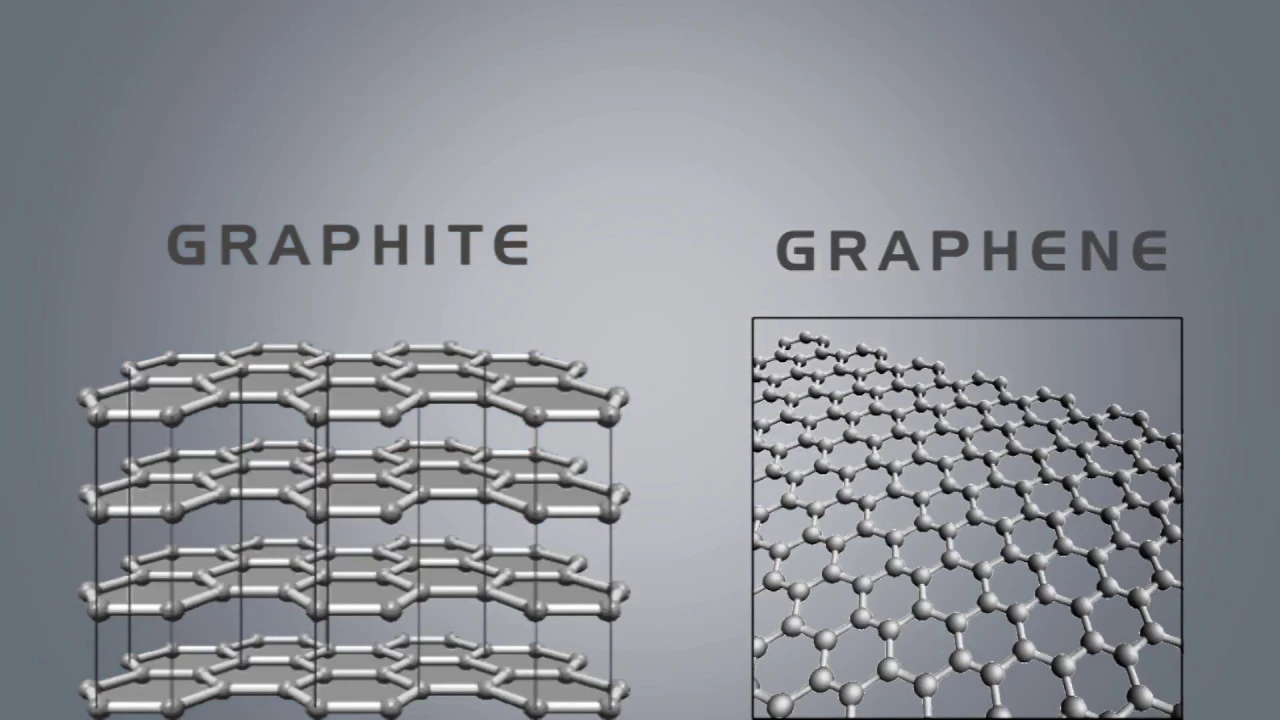
Difference Between Graphite and Graphene
63.5K
Graphite and graphene are both carbon-based materials with distinct structural differences: graphite consists of multiple layers of carbon atoms arranged in a hexagonal lattice, while graphene is a single layer of carbon atoms in the same hexagonal arrangement; this structural difference results in graphene being approximately 40 times stronger than diamond (130 GPa) and having superior electrical and thermal conductivity compared to graphite, making it ideal for advanced electronic and energy storage applications.
Click to watch →

Carbon Allotropes | Fullerenes | Graphites| Graphene | MSc.Chemistry Notes #chemistry
1.3K
Diamond and graphite represent two fundamentally different structural approaches to carbon bonding. Diamond features a three-dimensional tetrahedral network where each carbon atom bonds to four others, creating an exceptionally rigid and hard structure. In contrast, graphite consists of two-dimensional hexagonal layers where each carbon atom bonds to only three others within the plane, with weak van der Waals forces holding layers together. This structural difference explains their contrasting properties: diamond's rigidity makes it the hardest natural material, while graphite's layered structure allows easy layer separation, making it useful as a lubricant and electrical conductor.
Click to watch →
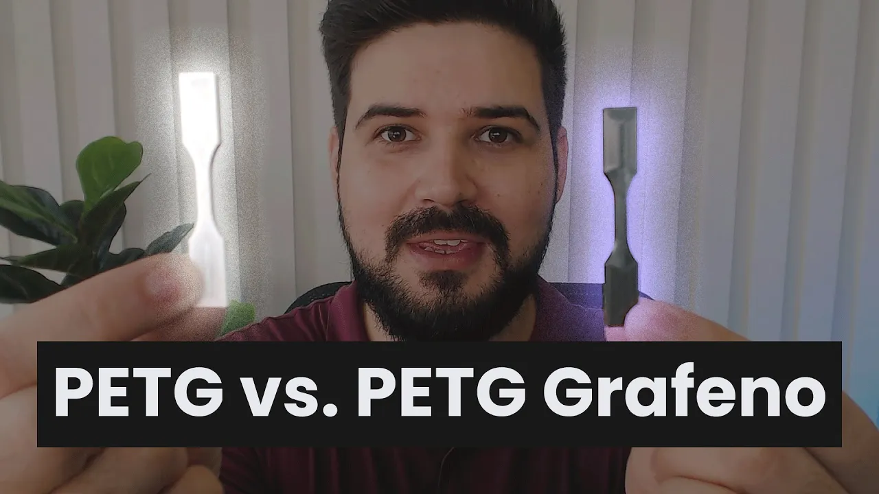
PETG Grafeno é REALMENTE mais resistente?
8.7K
Carbon exists in different atomic arrangements called allotropes, each with unique properties. Diamond has a tetrahedral 3D structure with each carbon bonded to four others. Graphite consists of hexagonal layers stacked together with weak interlayer bonds. Graphene is a single atomic layer of graphite, representing a 2D hexagonal carbon lattice. Graphene can be synthesized in laboratories through mechanical exfoliation or chemical oxidation of graphite. Graphene oxide, containing oxygen impurities, is commonly used in composites. These carbon allotropes demonstrate how atomic arrangement determines material properties.
Click to watch →
Deep Dive
The concept of Van der Waals forces and how these weak intermolecular bonds hold graphite layers together.
![ПИТАННЯ ВІД GOOGLE, НА ЯКЕ ВСІ ВІДПОВІДАЮТЬ НЕПРАВИЛЬНО 🤔 [VERITASIUM]](https://i.ytimg.com/vi/kZmvObHDuMs/maxresdefault.jpg)
ПИТАННЯ ВІД GOOGLE, НА ЯКЕ ВСІ ВІДПОВІДАЮТЬ НЕПРАВИЛЬНО 🤔 [VERITASIUM]
200.8K
Van der Waals forces are weak attractive forces between neutral atoms. When atoms are close together, electrons become unevenly distributed around the nucleus, creating temporary positive and negative charges on different sides of the atom. A nearby atom experiences this charge imbalance and develops an induced dipole. This creates a weak attraction between neutral atoms. These forces are responsible for gecko adhesion and also hold layers of graphite together in pencils.
Click to watch →
The Blender Question Everyone Gets Wrong
9.2M
Geckos can stick to walls due to Van der Waals forces, which are weak attractive forces between neutral atoms. When a gecko's foot presses against a surface, the atoms in the foot and the surface come within a few nanometers of each other. At any moment, an atom's electrons may not be uniformly distributed around its nucleus, creating temporary charge imbalances. These imbalances induce similar charge imbalances in neighboring atoms, causing electrons to be drawn toward opposite charges. This same force holds graphite layers together, though it is too weak for humans at normal scale.
Click to watch →
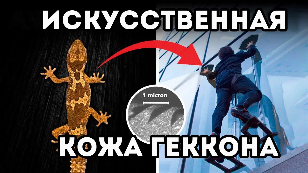
Самый липкий нелипкий материал (Veritasium)
496.4K
Geckos rely on Van der Waals forces for adhesion, which are weak attractive forces between neutral atoms. When atoms are very close (within nanometers), temporary charge imbalances occur due to uneven electron distribution, creating complementary charges that attract neighboring atoms. This force is too weak to notice with human fingers because our skin is too rough, but it becomes significant when contact area is maximized through the gecko's hierarchical structures.
Click to watch →

Complete Class 11th INORGANIC CHEMISTRY: Make Your Basics Super Strong || Lakshya JEE 2026🔥
390.2K
Van der Waals forces are weak intermolecular forces that include: (1) Dipole-dipole forces - between polar molecules; (2) Dipole-induced dipole forces - between polar and non-polar molecules; (3) London dispersion forces (induced dipole-induced dipole forces) - between non-polar molecules. These forces are directly proportional to molecular surface area. Larger molecules with greater surface area have stronger Van der Waals forces. The strength order is: dipole-dipole > dipole-induced dipole > London dispersion forces.
Click to watch →

Momentum Batch - 11th Chemistry :- L-06 परमाणु आकार-Atomic Size by Ashish sir
171.6K
When atoms do not form chemical bonds, they are held together by weak Van der Waals forces (also called London dispersion forces). These forces are much weaker than chemical bonds but are sufficient to bring atoms close enough to measure the Van der Waals radius.
Click to watch →
Deep Dive
Basic principles of optical microscopy and how light interference allows researchers to visualize atomically thin layers on a silicon dioxide substrate.
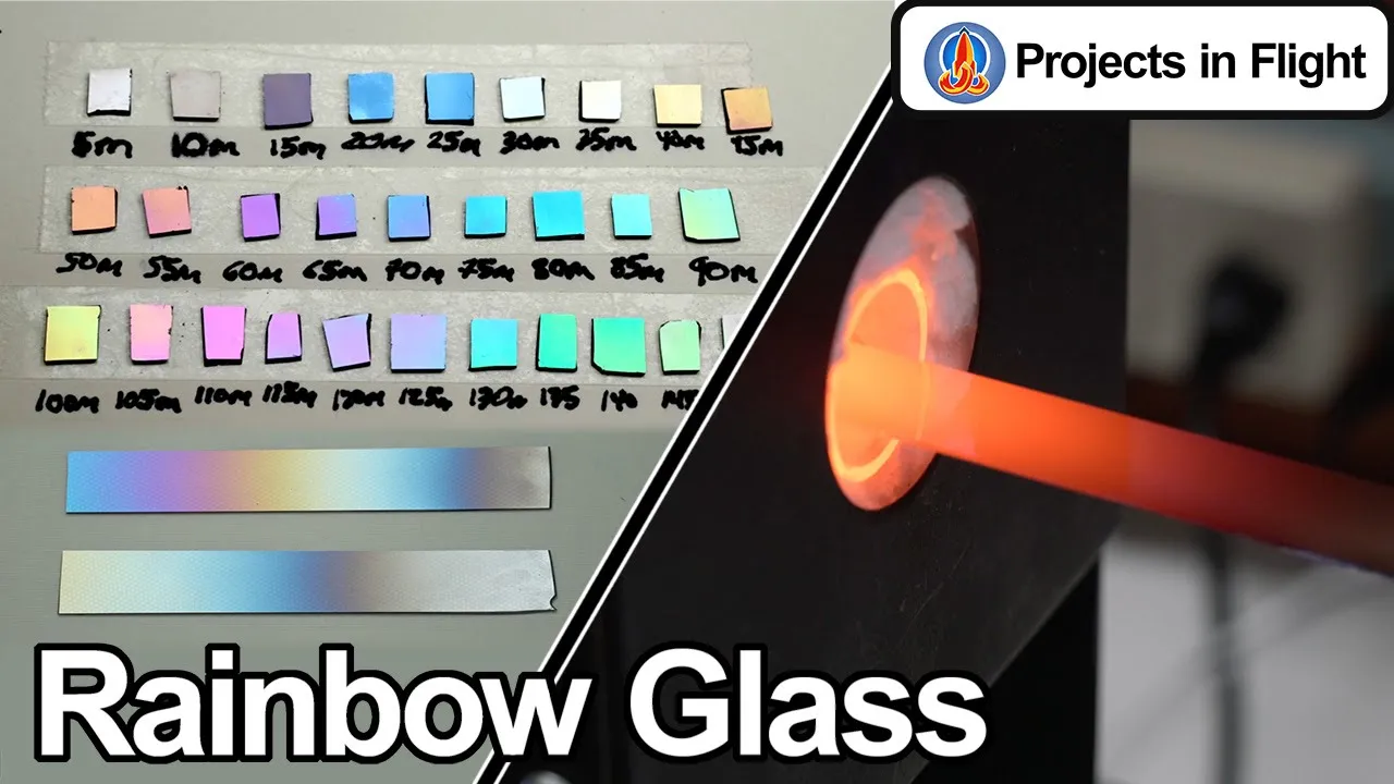
Growing Colorful Oxide Layers on Silicon
83.1K
Measuring oxide layer thickness at the nanoscale requires optical interference rather than microscopy. When light strikes a silicon wafer with an oxide layer, some reflects off the oxide surface while some penetrates and reflects off the underlying silicon. The silicon-reflected light travels a longer path, causing phase shifts between the two reflected beams. Since white light contains multiple wavelengths, constructive and destructive interference creates visible color changes. Thicker oxide layers produce different colors than thinner ones, allowing visual estimation of thickness. A reference chart correlates observed colors with approximate oxide thickness values, though accuracy is limited to ±25 nanometers for visual estimation.
Click to watch →
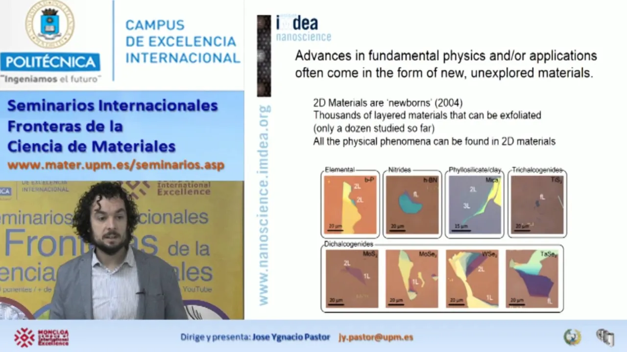
SFCM 15/16 7: TUTORIAL ON 2D CRYSTALS: SYNTHESIS, CHARACTERIZATION AND PROPERTIES
868
Optical interference colors allow identification of 2D material layer thickness. When light reflects off a thin dielectric film (like oil on asphalt), constructive and destructive interference creates rainbow colors depending on film thickness. Similarly, monolayer and few-layer 2D materials on silicon dioxide substrates produce distinct interference colors visible under optical microscopy, enabling rapid identification of desired layers.
Click to watch →
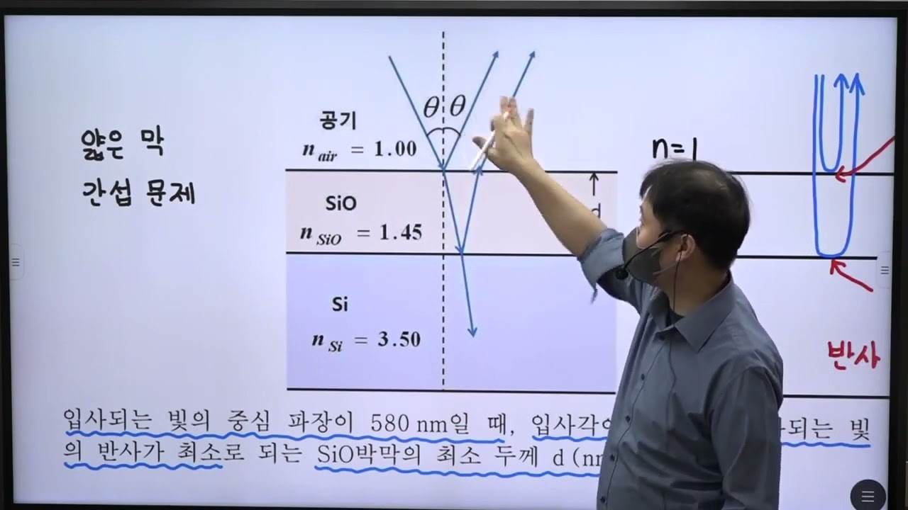
변리사 물리 기출 문제 풀이 50회 8번 2013년 8번 PA1308 / 물리 손용욱 강사 / 합격의 법학원 / 변리사1차 자연과학개론 / 변리사시험 / 변리사기출
638
When light reflects off a thin film coating, minimum reflection occurs when the reflected waves interfere destructively. For a silicon substrate (refractive index 3.5) coated with silicon dioxide (refractive index 1.45), with both reflections experiencing a 180° phase change, the condition for destructive interference is 2nD = (m + 1/2)λ. For minimum thickness (m=0), D = λ/(4n). Substituting λ = 580nm and n = 1.45 gives D = 100nm.
Click to watch →

2013-008:光マイクロマシンの原理
434
Optical interference occurs when two light waves interact constructively (amplifying each other) or destructively (canceling each other), and this principle enables advanced microscopy techniques that can observe internal structures of transparent materials by controlling light path lengths to isolate signals from specific depths, allowing for three-dimensional imaging of samples.
Click to watch →

「無反射多層基板を用いた光学的精密計測」神戸大学 大学院工学研究科 電気電子工学専攻 准教授 服部 吉晃
128
This technology enables atomic-level imaging using standard optical microscopes and digital cameras by utilizing a specially designed non-reflective multilayer substrate that exploits optical interference effects to detect extremely thin films (as thin as single atomic layers) through subtle color changes on the substrate surface, making advanced nanoscale measurements accessible without specialized equipment.
Click to watch →
Deep Dive
An introductory awareness of cleanroom protocols and contamination control, as dust can interfere with the transfer process.

Tại Sao Nhà Máy Chip Sạch Hơn Cả Phòng Mổ? Bí Mật Đằng Sau Những Con Chip Hiện Đại
180
Workers cannot simply change into uniforms and enter production areas. They must undergo extremely strict control procedures, changing all regular clothing for specially washed and packaged cleanroom attire. Inside production areas, touching the face, adjusting masks, or touching hair is prohibited. Cosmetics, perfumes, hairsprays, and strongly scented products are typically forbidden. Jewelry, watches, and bracelets must be removed to prevent dust accumulation or accidental damage. All equipment brought into cleanrooms must be cleaned and inspected. Wafer transport carts are made from special materials to minimize dust generation. Even writing materials are not ordinary—many facilities use low-dust paper or have switched entirely to electronic devices.
Click to watch →
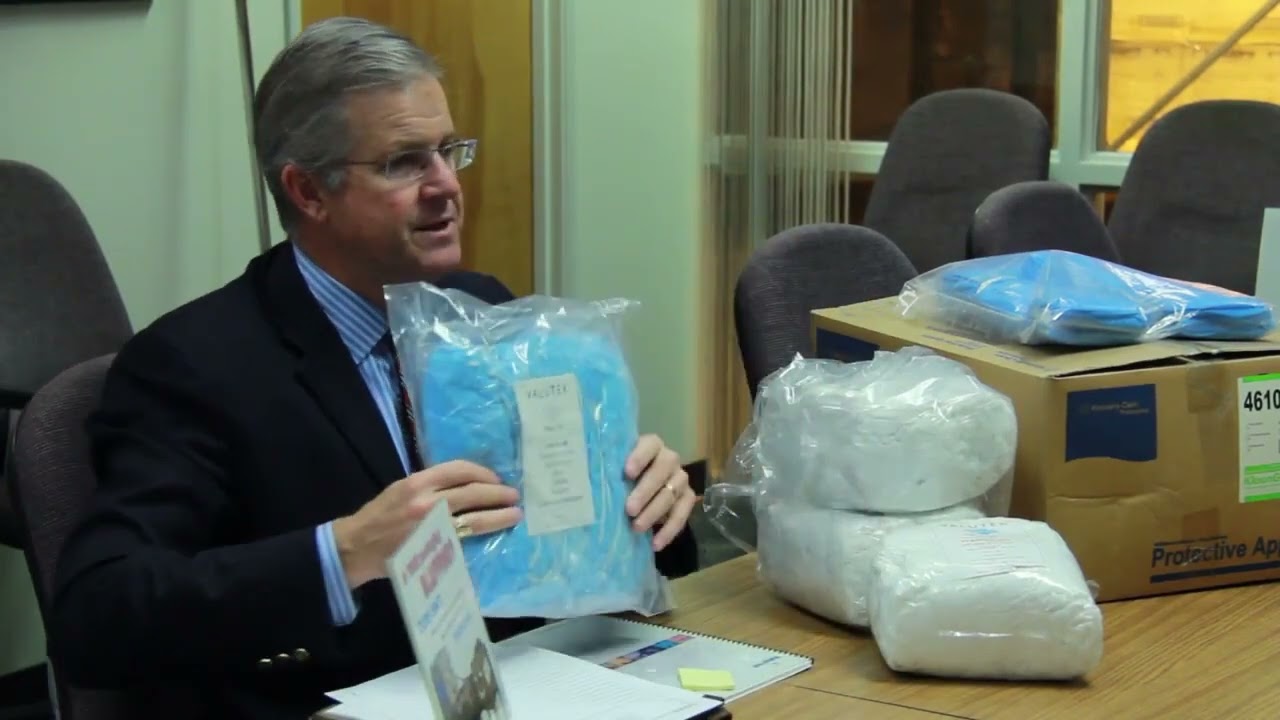
Non-Compliant Cleanroom Packaging: A Recipe for Contamination Control
189
Maintaining contamination control requires strict adherence to transfer protocols. Products must be opened in non-critical areas, removed from original packaging, and de-trashed before passing through controlled entry points. The pass-through system separates gown room environments from external areas. Inner bags are then taken into gown rooms for dispensing. This systematic approach prevents direct contact between external contaminants and cleanroom garments. Non-compliant packaging lacking liners or using uncoated materials creates unavoidable contamination risks during this transfer process.
Click to watch →
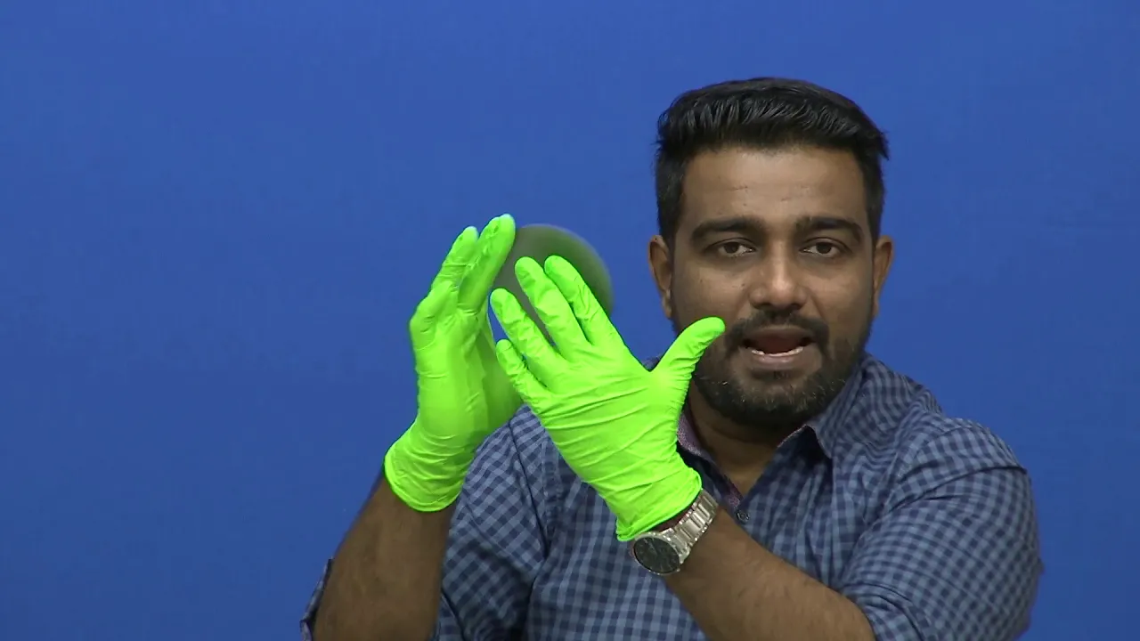
Introduction Wafer Manufacturing Process and Clean room Protocols
16.1K
Cleanroom environments require strict contamination control protocols since personnel are the primary contamination source. Effective gowning rooms and enforced procedures maintain required cleanliness classifications. Fundamental principles include: never letting clean surfaces contact dirty ones, washing hands thoroughly before touching clean materials, and garments never touching dirty floors. The gowning sequence follows a top-down approach: shoe cleaning with HEPA-filtered systems and rotating brushes, shoe cover application, hand washing and drying, glove liner and cleanroom glove application, hair/beard cover donning, hood and facemask application, coverall dressing using lean rails, and bootie placement with garment overlap. Garment materials range from disposable Tyvek/polypropylene to reusable Gore-Tex and ESD-specific fabrics. Storage cabinets feature HEPA filtration for maintaining garment cleanliness. Personnel must perform visual self-checks using mirrors before entering cleanrooms. Single-side polished wafers are more economical than double-side variants. Understanding these protocols ensures device reliability and high fabrication yields in semiconductor manufacturing facilities.
Click to watch →

Cleanroom contamination control, as illustrated with an onion
4.7K
Cleanroom contamination control operates on a concentric zone system where multiple protective layers progressively increase in stringency from the outermost area (Grade D) to the innermost critical zone (Grade A), similar to how an onion's outer layers protect its core; this multi-layered approach includes controlled non-classified areas, changing rooms with particle dissipation protocols, and airlock systems for material transfer, all working together to minimize contamination risks throughout the facility.
Click to watch →

Cleanroom Training Video
371.2K
Cleanrooms are controlled environments where airborne particle quantity and size are meticulously managed using HEPA filtration systems, classified under ISO 14644 standards from Class 1 (cleanest) to Class 9 (least clean); proper operation requires thorough preparation including removing prohibited items like paper and cardboard, wiping all surfaces with approved solvents, and following a systematic gowning procedure from top to bottom (bonnet cap, face mask, smock or bunny suit, gloves) before entering, then working slowly to minimize particle release and de-gowning in reverse order upon exit.
Click to watch →
Prerequisite Knowledge
- Concept 01Understanding the atomic structure of carbon allotropes, specifically the structural difference between 3D graphite and 2D graphene.
- Concept 02The concept of Van der Waals forces and how these weak intermolecular bonds hold graphite layers together.
- Concept 03Basic principles of optical microscopy and how light interference allows researchers to visualize atomically thin layers on a silicon dioxide substrate.
- Concept 04An introductory awareness of cleanroom protocols and contamination control, as dust can interfere with the transfer process.
Subsequent Learning
- Step 01Advanced characterization techniques, such as Raman Spectroscopy and Atomic Force Microscopy (AFM), to identify and verify single-layer graphene.
- Step 02Alternative, scalable synthesis methods of graphene, including Chemical Vapor Deposition (CVD) and liquid-phase exfoliation.
- Step 03Device fabrication techniques, such as lithography, to utilize exfoliated graphene in making field-effect transistors (FETs).
- Step 04Exploring the electrical, thermal, and mechanical properties of graphene that make it a candidate for next-generation nanoelectronics and composites.
Graphite Exfoliation
Graphite Exfoliation
0:04Playing Section
- 1
Peel graphite flakes using tape until thin.
- 2
Transfer flakes to silicon wafer by rubbing.
- 3
Identify graphene via optical purple spots.
Chemical Vapor Deposition and Bulk Production for Industrial Scalability
While the Scotch tape method (mechanical exfoliation) is historically significant and produces exceptionally high-quality, defect-free graphene ideal for fundamental laboratory research, it is fundamentally unsuited for commercial or industrial applications. It is a manual, labor-intensive, and low-yield process that cannot produce large-area graphene sheets consistently or cost-effectively. To transition graphene into practical technologies, alternative production methods are necessary. Chief among these is Chemical Vapor Deposition (CVD), which enables the growth of large-area, continuous graphene films on metal substrates (like copper) for electronics and sensors. For bulk applications like composites, batteries, and conductive inks, liquid-phase exfoliation and the reduction of graphene oxide offer scalable, high-throughput chemical alternatives. These scalable synthesis methods prioritize throughput, cost-efficiency, and uniformity over the artisanal, single-flake precision of the Scotch tape technique.
Deep Dive
Advanced characterization techniques, such as Raman Spectroscopy and Atomic Force Microscopy (AFM), to identify and verify single-layer graphene.
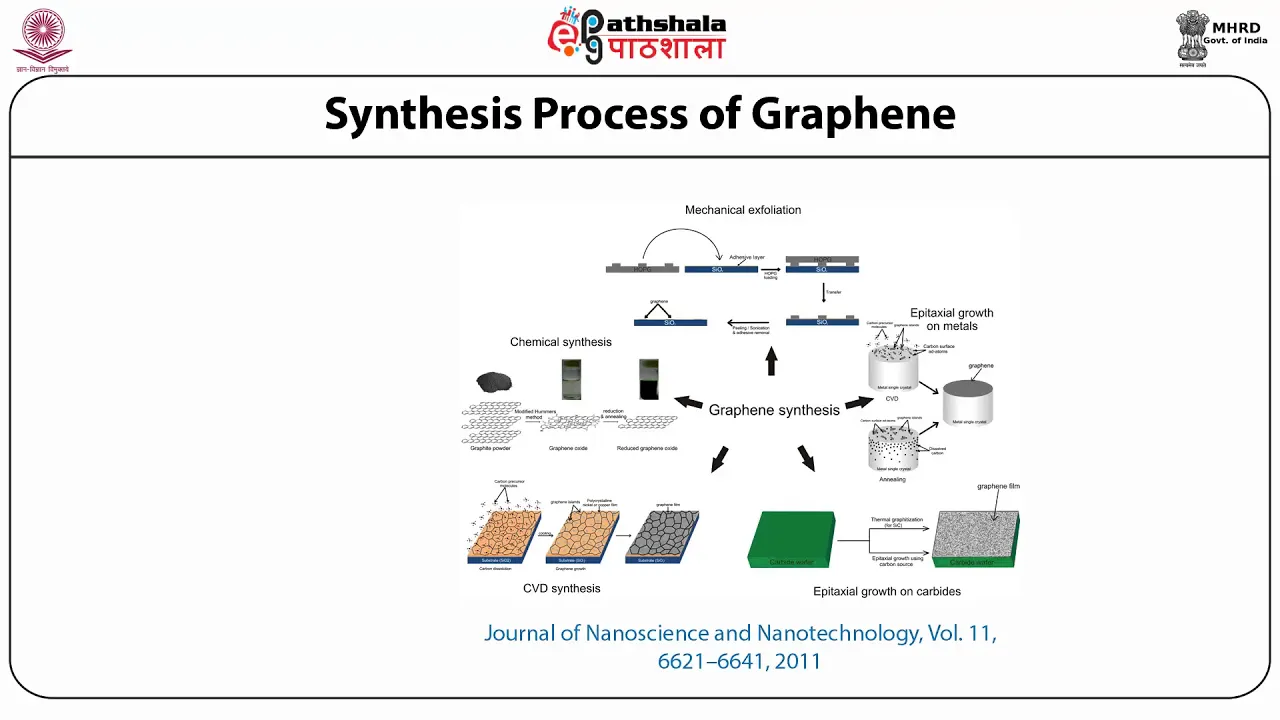
Introduction, Synthesis and Characterizations of Graphene
12.3K
Raman spectroscopy is a vibrational technique extremely sensitive to geometrical structure and bonding within molecules. Small differences in geometrical structure lead to significant differences in observed Raman spectra. For graphene, the technique can differentiate between single-layer, double-layer, triple-layer graphene, and graphite based on the position, shape, and relative intensity of characteristic bands. Raman spectroscopy can determine graphene layer thickness at atomic-level resolution for samples with fewer than four layers, which is crucial for current graphene research.
Click to watch →
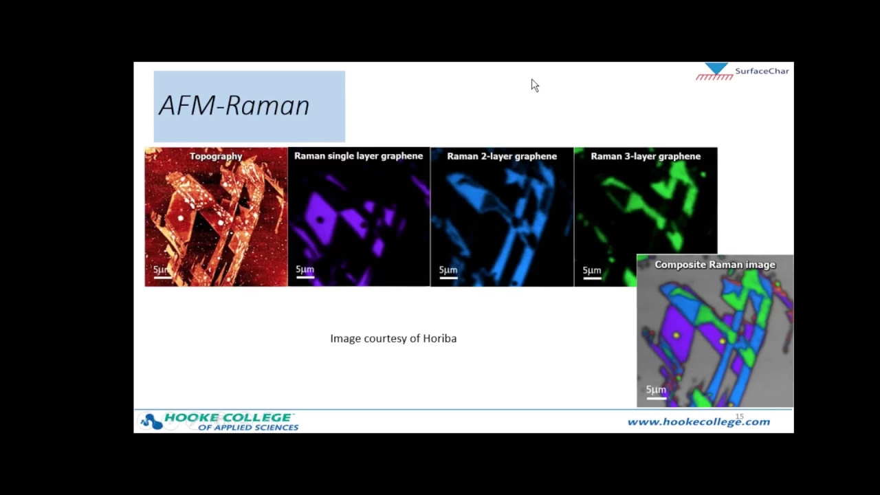
More Than Topography: What Else Can Atomic Force Microscopy Measure?
692
Atomic Force Microscopy integrates chemical and spectroscopic characterization through co-localized measurements. Combining AFM with confocal Raman spectroscopy enables identification of different graphene layer counts (single, double, triple layers) through distinct Raman spectral signatures, mapping their spatial distribution impossible with topography alone. Tip-enhanced Raman spectroscopy achieves even higher resolution. For infrared characterization, AFM-IR overcomes the diffraction limit (typically limiting conventional IR to micrometer resolution) to achieve sub-100 nanometer resolution using either apertureless scattering methods or photo-thermal detection. Applications include mapping protein distributions (1650 cm⁻¹ peak) and triglyceride distributions (1740 cm⁻¹ peak) in bacteria, and distinguishing polymer components (PMMA vs polystyrene) in diblock copolymer thin films. Multi-modal AFM combining topography, phase imaging, KPFM, and Raman spectroscopy provides comprehensive characterization of complex nanomaterials.
Click to watch →
Graphene Characterization Methods and Issues - Dr. Andrew Pollard National Physical Laboratory NPL.
2K
Multiple complementary techniques characterize graphene structure: Raman spectroscopy identifies layer count and disorder through optical analysis; SEM reveals lateral flake size distribution through electron imaging; AFM measures thickness via scanning probe microscopy; TEM provides high-resolution layer counting through diffraction patterns. Each technique has strengths and limitations—Raman is fast but requires careful interpretation, while TEM offers precision at higher cost. Sample preparation critically affects all measurements, requiring isolation of individual flakes for accurate results.
Click to watch →

Making Graphene could KILL you... but we did it anyway?!
2.4M
Raman spectroscopy identifies graphene by shining a laser on a surface and analyzing scattered photons. While 99%+ of light is scattered, reflected, or absorbed, a tiny fraction interacts with molecular bonds. Photons may be red-shifted (losing energy to bonds) or blue-shifted (gaining energy from bonds). The degree of shift is exquisitely sensitive to bond nature and environment. Different carbon bonds (O-bond in water vs methanol/ethanol, C-C bonds in graphene interior vs edges, and stacked graphene vs single layers) produce distinct peaks. This technique distinguishes graphene from graphite and other carbon forms.
Click to watch →
Spectroscopy in Graphene - Andrea Ferrari
4.1K
Raman spectroscopy enables non-destructive characterization of graphene by analyzing the energy loss when light interacts with graphene's atomic lattice, allowing researchers to determine key properties such as layer number, doping levels, strain, defects, and functionalization without damaging the sample; this technique, developed in 2004, has become the standard method for graphene identification across all laboratories and companies worldwide, facilitating both fundamental research and industrial mass production of graphene materials.
Click to watch →
Deep Dive
Alternative, scalable synthesis methods of graphene, including Chemical Vapor Deposition (CVD) and liquid-phase exfoliation.
Making Graphene could KILL you... but we did it anyway?!
2.4M
Two main approaches exist for graphene production. Top-down methods start with graphite and separate graphene: mechanical exfoliation (tape peeling) works in labs but isn't scalable; electrochemical exfoliation uses electrical current to separate layers but contaminates graphene. Bottom-up methods grow graphene from carbon atoms: Chemical Vapor Deposition (CVD) uses plasma to deposit graphene on copper substrates, leveraging the most stable carbon-carbon bond, but produces only picogram quantities with expensive equipment. Rice University's flash graphene represents an innovative middle ground—using simple equipment to heat carbon sources to 3100K and rapidly cool to form turbostratic graphene that can be easily exfoliated, achieving production rates orders of magnitude higher than CVD.
Click to watch →

Графен: Материал будущего, который прочнее алмаза в 200 раз!
882
Mechanical exfoliation (the scotch tape method) produces graphene of the highest quality - monocrystalline flakes up to several hundred micrometers in size, nearly defect-free, with electronic properties closest to theoretical predictions. However, productivity is only a few flakes per session - industrial scale is impossible. Chemical Vapor Deposition (CVD) is the main candidate for industrial production. The process involves placing copper foil in a reactor, heating it to 1,000°C, and passing methane and hydrogen through it. Methane decomposes on copper, and carbon atoms self-assemble into a hexagonal lattice. Copper acts as catalyst, substrate, and limiting factor - its surface is catalytically active only for the first monolayer. A key 2010 breakthrough demonstrated roll-to-roll production of graphene 30 inches wide. However, CVD graphene grows on copper, which must be dissolved, leaving graphene floating on liquid surface held only by a polymer support film. Any mechanical stress creates cracks, wrinkles, and tears. In real CVD films, defect density is several orders of magnitude higher than in exfoliated flakes. Liquid phase exfoliation is the dominant commercial method, using natural graphite (the same material in pencils and batteries) with shear force in solvents to create flakes 1-30 layers thick. This method scales easily and cheaply but never produces monolayers - it produces thin graphite, not graphene. Epitaxial growth on silicon carbide eliminates the transfer step entirely, growing graphene directly on a dielectric substrate. When heated to 1,400°C in vacuum, silicon evaporates and remaining carbon reconstructs into a graphene lattice. This is most promising for semiconductor integration because silicon carbide is compatible with standard processes. Environmental assessment shows CVD is energy-intensive due to high temperatures, liquid phase exfoliation is chemically intensive due to solvent use, and epitaxial growth is the most energy-intensive. At industrial volumes, these factors become significant for sustainability.
Click to watch →
Introduction, Synthesis and Characterizations of Graphene
12.3K
Producing high-quality graphene requires reliable methods for growing continuous single and few-layer films. Top-down approaches reduce bulk graphite to smaller pieces: mechanical exfoliation (Scotch tape method) exploits weak van der Waals forces to peel monolayers, first demonstrated by Novoselov and Geim in 2004, but yields insufficient quantities for commercial use. Liquid phase exfoliation suspends graphite in solvent and applies ultrasound, producing larger quantities but generating mixed samples with defects. Bottom-up approaches build graphene from atoms: epitaxial growth and chemical vapor deposition (CVD) on transition metal substrates enable scalable production of centimeter-long continuous films. CVD using liquid precursors like hexane offers advantages over gas precursors (methane, ethylene) through easier handling, lower cost, and simpler doping capabilities using nitrogen/boron-containing solvents.
Click to watch →

Graphene science | Mikael Fogelström | TEDxGöteborg
748.1K
Chemical vapor deposition (CVD) is a scalable method for producing large-area graphene films. The process involves placing a hot metal substrate (such as copper) in a furnace and introducing carbon-containing gases. The gas molecules dissociate and carbon atoms deposit onto the metal surface, self-assembling into a single layer of graphene. This technique has enabled production of graphene sheets up to 20 cm in size, suitable for commercial applications.
Click to watch →

꿈의 신소재 그래핀, 이게 문제입니다 (한국전기연구원 김정모 선임연구원)
89K
Graphene production uses two main methods: mechanical exfoliation and chemical vapor deposition (CVD). Mechanical exfoliation, also known as the 'Scotch tape method,' involves repeatedly peeling graphite with adhesive tape to isolate single layers. This method, discovered by Andre Geim and Konstantin Novoselov (Nobel Prize winners), produces the highest quality graphene with the best crystallinity. CVD involves growing graphene on metal substrates like copper or nickel by exposing them to carbon-containing gases at high temperatures. CVD can produce larger areas but requires specialized equipment. The choice between methods depends on whether quality or quantity is prioritized.
Click to watch →
Deep Dive
Device fabrication techniques, such as lithography, to utilize exfoliated graphene in making field-effect transistors (FETs).

Physics@FOM Veldhoven 2011, Bart van Wees, Master class I
2.8K
Graphene devices are fabricated using electron beam lithography to create metal contacts on graphene flakes. The gate electrode is typically highly doped silicon, which behaves like a metal. Applying a gate voltage creates an electric field that induces charge carriers in the graphene, allowing control of the carrier density. The resulting field effect transistor shows a characteristic resistance curve with a maximum at the neutrality point (Dirac point), where the Fermi level sits at the band crossing. The minimum conductivity at this point is approximately 4e²/h, a universal value determined by fundamental constants.
Click to watch →

Graphene for energy harvesting applications — Zhenxing Wang
132
Graphene's exceptional properties—including high carrier mobility, thinness, flexibility, strong bonding, chemical inertness, and large-scale synthesizability—make it ideal for advanced electronics. Four synthesis methods exist: mechanical exfoliation (Nobel Prize-winning method, high quality but not scalable), chemical exfoliation/reduction, CVD on copper, and architectural growth on silicon carbide. Plotting price versus quality reveals CVD as optimal for scalable production. However, CVD graphene requires transfer from copper substrates, introducing residues that degrade device performance. Two production approaches exist: wafer-scale methods using eight-inch wafers for round graphene sheets, and road-to-road processes for continuous production yielding square graphene requiring further cutting. Graphene field effect devices are fabricated through sequential lithography, plasma etching, and metal deposition processes. Silicon/silicon oxide substrates serve as global back-gates to tune device resistance. Despite excellent transport properties, graphene lacks a band gap, preventing complete switching off. This results in V-shaped transfer curves with saturation at high fields and characteristic kinks in output curves, making traditional graphene field effect transistors unsuitable for digital switching applications.
Click to watch →

Layout Editor Tutorial 01: Introduction
17.6K
This tutorial introduces the fundamentals of laying out graphene field-effect transistors (FETs) and test devices on purchased graphene wafers using layout editor software. The graphene wafer consists of a 100mm p-doped silicon substrate with 285-300nm silicon dioxide dielectric, topped with CVD-grown graphene. Key design rules include 160-micron saw lanes, 110-micron pad-to-saw center distance, 180-micron spacing between dies, 100-micron square bonding pads, 1-micron trace width, and 1-micron trace-to-trace spacing. The fabrication process involves depositing a top dielectric layer using atomic layer deposition (ALD), followed by photolithography steps where Mask 1 removes dielectric and graphene to form device structures, Mask 2 removes dielectric to expose graphene for contacts, and Mask 3 patterns metal contacts for source, drain, and gate electrodes. The wafer includes various test structures such as Hall bar structures for measuring resistivity, carrier density, and Hall mobility, van der Pauw structures for resistivity measurement, and contact resistance structures for evaluating sheet resistance, contact resistivity, and transfer length.
Click to watch →

Pasqualantonio Pingue, Daniele Ercolani - Superstar graphene - 11 ottobre 2013
498
Natural graphite from Canadian mines consists of stacked graphene sheets like book pages. Scanning Tunneling Microscopy (STM) uses quantum tunneling to image individual atoms, revealing graphene's hexagonal lattice structure. Chemical Vapor Deposition (CVD) grows graphene on copper using methane decomposition, creating ordered hexagonal lattices. The first carbon layer saturates the copper surface, enabling self-limiting single-layer growth. Liquid exfoliation creates graphene inks separable by ultracentrifugation for inkjet printing. Electron beam lithography deposits nanoscale contact pads for device fabrication, enabling electrical measurements of graphene's properties for transistors and electronic devices.
Click to watch →

Jeanie Lau: Graphene -- The Amazing 2D Membrane
164
Graphene transistors are fabricated using lithography techniques similar to those in the semiconductor industry but adapted for the nanoscale. The process involves depositing a resist layer on graphene, exposing it to electron beams (which have very short wavelengths for precise patterning), developing the resist to remove exposed areas, and then evaporating metal to create electrodes. The resulting device consists of source and drain electrodes connected to a gate electrode that controls the number of charge carriers (electrons or holes) in the graphene channel. This allows researchers to measure electrical transport properties and study how electrons move through the graphene material under controlled conditions.
Click to watch →
Deep Dive
Exploring the electrical, thermal, and mechanical properties of graphene that make it a candidate for next-generation nanoelectronics and composites.
#25 Graphene | A 2D Nanomaterials | Nanotechnology, Science and Applications
14.7K
Graphene possesses a unique zero band gap electronic structure where conduction and valence bands touch, making it a semimetal with exceptional electron mobility exceeding copper's conductivity. A single layer is nearly transparent with 2-3% light absorption, increasing proportionally with layer count. Graphene exhibits ferromagnetic behavior at room temperature, with properties strengthening as layer count decreases due to edge effects and potential magnetic impurities. Mechanically, graphene has Young's modulus one order of magnitude higher than steel and tensile strength two to three orders of magnitude greater than steel or aluminum, yet maintains a low density of approximately 2.2 g/cm³. Thermally, graphene possesses exceptionally high thermal conductivity comparable to or exceeding diamond, resulting from strong covalent bonds facilitating efficient phonon transfer. Unlike diamond, graphene conducts both heat and electricity effectively due to its unique electronic structure.
Click to watch →
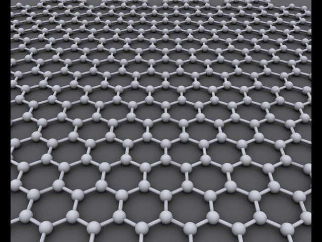
Graphene | Wikipedia audio article
112
Graphene exhibits remarkable optical properties including saturable absorption across visible to near-infrared wavelengths due to universal optical absorption and zero band gap, enabling full-band mode locking in fiber lasers. The nonlinear Kerr coefficient is 10⁻⁷ cm²·W⁻¹, nine orders of magnitude larger than bulk dielectrics. Thermal transport is phonon-dominated with Wiedemann-Franz law applicability. Early measurements reported 5300 W·m⁻¹·K⁻¹ for suspended graphene, later refined to 1500-2500 W·m⁻¹·K⁻¹. When supported on amorphous materials, thermal conductivity drops to ~500-600 W·m⁻¹·K⁻¹ due to substrate scattering. Graphene has three acoustic phonon modes: two in-plane (LA, TA) with linear dispersion and one out-of-plane (ZA) with quadratic dispersion. At low temperatures, T¹·⁵ contribution from ZA modes dominates thermal conductivity. Some phonon bands display negative Grüneisen parameters, causing negative thermal expansion coefficient. The membrane effect predicts phonon frequency increases with in-plane lattice parameter upon stretching. Graphene has carbon-carbon bond length of ~0.142 nm and interplanar spacing of 0.335 nm in graphite. It is the strongest material ever tested with intrinsic tensile strength of 130.5 GPa and Young's modulus of 1 TPa. Despite this strength, graphene is relatively brittle with fracture toughness of ~4 MPa√m, cracking in brittle manner like ceramics. The Mermin-Wagner theorem shows long-wavelength fluctuation amplitude grows logarithmically with scale in 2D structures, making them unbounded in infinite systems. Graphene's melting point was predicted at ~4125 K, later increased to at least 5000 K through sophisticated modeling.
Click to watch →

SAMSUNG SECRET: $28 Silver Collapse (SEC Filing: 340M Oz Hidden Stockpile, Graphene Replaces Silver)
42.8K
Graphene conductors exhibit superior properties compared to silver: electrical conductivity of 118% of silver (meaning electrons move more efficiently), thermal conductivity of 93% of silver (slightly lower but acceptable for all applications), and flexibility superior to silver. These properties create design advantages including smaller circuits, thinner devices, and reduced power consumption. The cost advantage is 97% cheaper than silver, making it economically compelling even if silver prices collapse to $28.
Click to watch →
Graphene science | Mikael Fogelström | TEDxGöteborg
748.1K
Graphene is the best thermal conductor known, carrying heat extremely efficiently. It is also one of the best electrical conductors, carrying electric charge with exceptional efficiency. Combined with its transparency, these properties enable numerous technological applications. For example, 15 kilograms of graphene could potentially cover all computer displays and iPad screens worldwide, demonstrating both its abundance and versatility for electronic applications.
Click to watch →
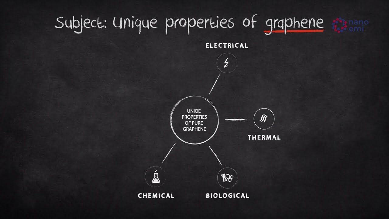
Unique properties of graphene - mechanical - electrical - optical - thermal - chemical - biological
783
Graphene possesses exceptional mechanical strength (high Young's modulus), electrical conductivity, optical transparency, thermal conductivity, chemical reactivity, and biological compatibility, making it a versatile material for applications ranging from electronics and composites to biomedical technologies.
Click to watch →
Graphite Exfoliation
Graphite Exfoliation
0:04- 1
Peel graphite flakes using tape until thin.
- 2
Transfer flakes to silicon wafer by rubbing.
- 3
Identify graphene via optical purple spots.
Chemical Vapor Deposition and Bulk Production for Industrial Scalability
While the Scotch tape method (mechanical exfoliation) is historically significant and produces exceptionally high-quality, defect-free graphene ideal for fundamental laboratory research, it is fundamentally unsuited for commercial or industrial applications. It is a manual, labor-intensive, and low-yield process that cannot produce large-area graphene sheets consistently or cost-effectively. To transition graphene into practical technologies, alternative production methods are necessary. Chief among these is Chemical Vapor Deposition (CVD), which enables the growth of large-area, continuous graphene films on metal substrates (like copper) for electronics and sensors. For bulk applications like composites, batteries, and conductive inks, liquid-phase exfoliation and the reduction of graphene oxide offer scalable, high-throughput chemical alternatives. These scalable synthesis methods prioritize throughput, cost-efficiency, and uniformity over the artisanal, single-flake precision of the Scotch tape technique.
Understanding the atomic structure of carbon allotropes, specifically the structural difference between 3D graphite and 2D graphene.
The concept of Van der Waals forces and how these weak intermolecular bonds hold graphite layers together.
Basic principles of optical microscopy and how light interference allows researchers to visualize atomically thin layers on a silicon dioxide substrate.
An introductory awareness of cleanroom protocols and contamination control, as dust can interfere with the transfer process.
Advanced characterization techniques, such as Raman Spectroscopy and Atomic Force Microscopy (AFM), to identify and verify single-layer graphene.
Alternative, scalable synthesis methods of graphene, including Chemical Vapor Deposition (CVD) and liquid-phase exfoliation.
Device fabrication techniques, such as lithography, to utilize exfoliated graphene in making field-effect transistors (FETs).
Exploring the electrical, thermal, and mechanical properties of graphene that make it a candidate for next-generation nanoelectronics and composites.
350.2K views467likes1:45@tetrflareOriginal Release: 2009-06-03
Take a scotch tape and gently lay it down on a flat surface. Next, take clean metal tweezers and pick a thin graphite flake and then place this gently onto the scotch tape.
Next, fold the scotch tape at the edge of the graphite flake.
Peel it off gently and do this step several times until you obtain a nearly transparent region on the scotch tape.
After this, take a clean silicon wafer to transfer the scotch tape graphine onto the wafer. Use plastic tweezers and gently rub the area of the scotch tape where graphine may potentially be.
Slowly peel off the scotch tape so as not to break any potential graphine sheets. Use an optical microscope to view and find graphine.
Graphine appears as a purple spot on the screen. At the center of the screen is multi-layer graphine and at the right corner lower right corner of the screen is single layer graphine.
Up Next

53:35
Introduction to Metal-Organic Frameworks: Synthesis & Applications
@SOORIYAOLI
4.7K views•2020-07-08

83:56
Biocatalysis and Catalysis in Islatravir Synthesis | Merck Webinar
@SCIwheresciencemeetsbusiness
675 views•2020-10-08
10:06
1H NMR: Determining Number of Peaks from Structure
@MSJChem
59.2K views•2017-04-06
17:31
Edible Water Bottles: A DIY Guide to Sodium Alginate Spherification
@ryan
10.5M views•2019-06-21
Related Study Plans & Knowledge Roadmaps
Structured learning paths in Chemistry
chemistry
Nuclear Chemistry: Decay, Meds & Fuel Cycle
01Introduction to Nuclear Structure and Radioactivity
02Decay Dynamics and Kinetics
03Radiation Interaction and Detection
+ 2 more learning modules
24h5 modules
Explore Roadmap
chemistry
Supramolecular Chemistry: Forces & Machines
01Foundations of Chemical Bonding and Intermolecular Forces
02Introduction to Host-Guest Chemistry
03Thermodynamics and Dynamics of Self-Assembly
+ 2 more learning modules
16h5 modules
Explore Roadmap
chemistry
Photochemistry: Excited States & Reactions
01Foundations of Light-Matter Interactions
02Molecular Orbitals and Electronic States
03Photophysical Processes and Jablonski Diagrams
+ 2 more learning modules
18h5 modules
Explore Roadmap
chemistry
Coordination Chemistry: Bonding & Properties
01Introduction to Transition Metals and Ligands
02Crystal Field Theory (CFT) and Geometry
03Magnetic Behavior and Spin States
+ 2 more learning modules
14h5 modules
Explore Roadmap