














![El diodo semiconductor [Curso de Electronica 1]](https://i.ytimg.com/vi_webp/mwohMU5qACg/maxresdefault.webp)


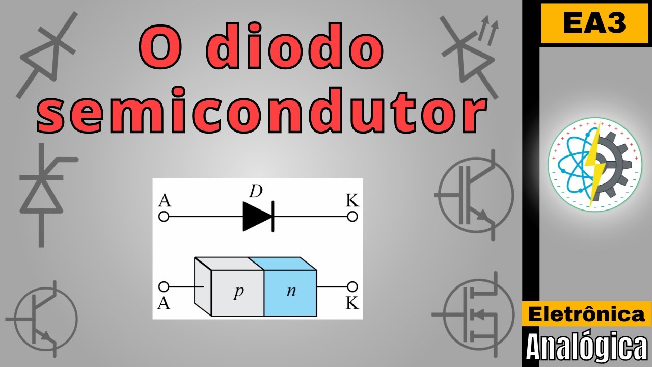








In forward bias condition of a PN junction diode, connecting the positive terminal of a battery to the P-side and the negative terminal to the N-side causes holes and electrons to be repelled toward the depletion layer, where they recombine with ions, reducing the width of the depletion layer and lowering the barrier potential; this enables majority carriers to cross the junction, resulting in a significant increase in diode current that rises exponentially as the applied voltage approaches the barrier potential (approximately 0.7V for silicon), while the reverse saturation current remains constant as it depends only on temperature and minority carrier concentration.
PN Junction Diode Forward Bias Operation Explained
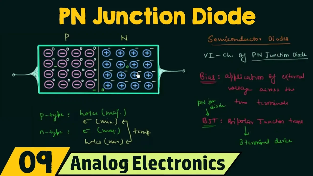
Added:Basic semiconductor physics, including the concept of doping to create P-type and N-type materials with majority and minority charge carriers.
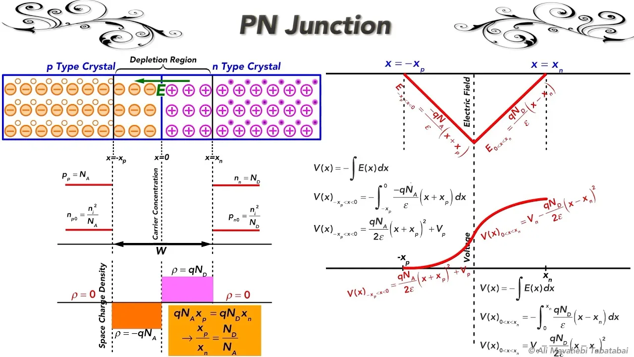
The formation of a PN junction in thermal equilibrium, specifically the diffusion of carriers and the resulting depletion region.
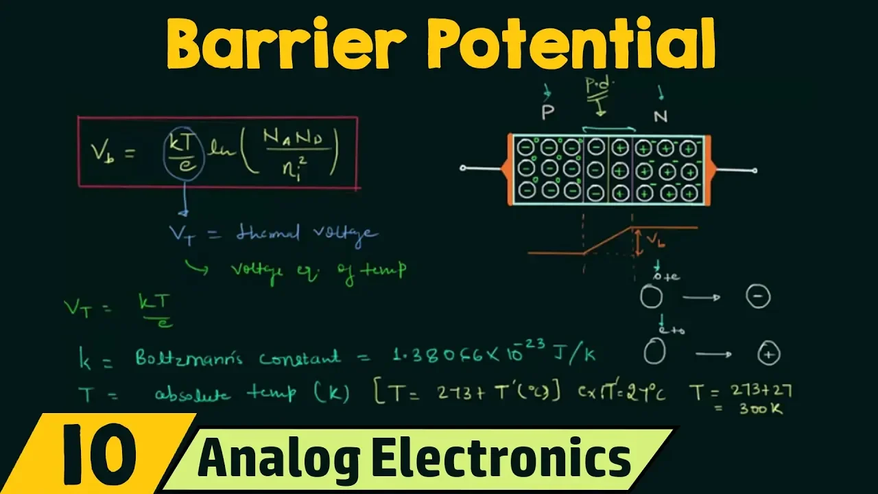
The concept of barrier potential (built-in potential) and the internal electric field established across the depletion layer.
Fundamental circuit concepts, such as electric potential, voltage polarity, and how external electric fields influence charge carriers.
PN junction operation under Reverse Bias conditions, including the widening of the depletion layer and junction breakdown mechanisms.
The Diode I-V Characteristic Curve and the Shockley diode equation, which mathematically models the exponential current flow.
Practical applications of diodes in electronic circuits, such as half-wave and full-wave rectification.
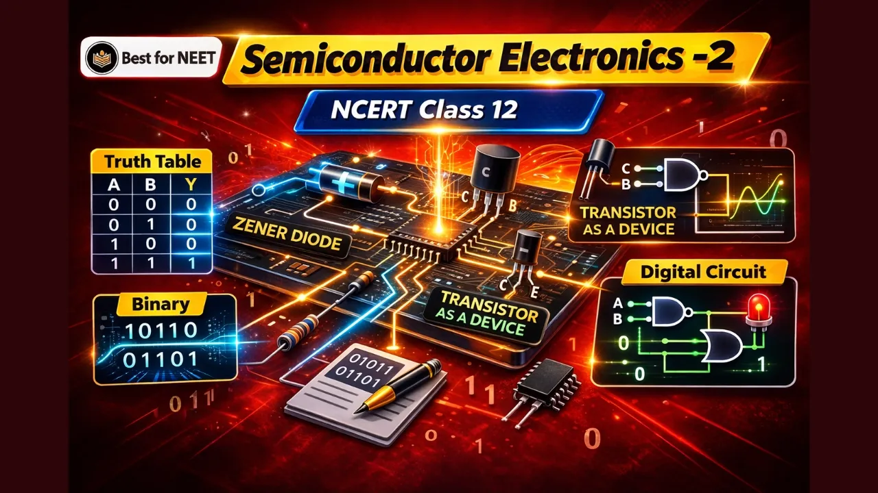
The operating principles of specialized optoelectronic and semiconductor devices, such as Light Emitting Diodes (LEDs), Zener diodes, and solar cells.
764.2K views7.1Klikes8:38Original Release: 2016-03-23
We have already completed no bias condition of P and junction diode. In this lecture, we will discuss forward bias condition of P and junction diode.
Under no bias condition, we do not apply any external voltage source across these two terminals. So, this is the case of no bias condition. And let's say and let's say the width of depletion layer width of depletion layer is W subscript D. And this is the junction. This is the junction.
And we have diffusion current from left to right. We have diffusion current from left to right.
And I will call it I majority. And we have reverse saturation current from right to left. This is I subscript S.
And reverse saturation current is due to the minority charge carriers. Now in forward bias condition, we connect positive terminal of the battery to the P side and we connect negative terminal of the battery to the N side of the P and junction diode. So I will do this quickly.
I will do this quickly.
This is the positive terminal of the battery and this is the negative terminal of the battery. And I will connect the positive terminal to the P side of the P and junction diode. And I will connect negative terminal to the N side of the P and junction diode. Now because of this because of this the holes on P side will be repelled because holes are positively charged and we have holes as majority charge carriers on P side. This positive terminal of the battery will repel the holes towards the depletion layer and in the same way negative terminal of the battery will repel the electrons towards the depletion layer because electrons are negatively charged. Thus we can say that the forward bias potential WD the forward bias potential WD will pressure the electrons on N side and holes on P side to recombine with the ions near the boundary and reduce the width of depletion reason. So the width of depletion reason will reduce because the holes will combine with the negative ions and electrons will recombine with the positive ions. So we have we have holes recombined with the negative ions and we have electrons we have electrons combined with the positive ions and as you already know in depletion layer we do not have mobile charge carriers but we have immo ions. So the width of depletion layer will reduce and we have a new depletion reason and let's say the width is the width is this is the new width and I will call it WD prime. So we have new width equal to WD prime and if I compare it with no bias condition then W D was equal to zero and the width of depletion reason was W subscript D and when V D is greater than zero it means it is positive the new width is WD prime and if we compare WD and WD prime we will find WD is greater than WD prime. So we can say that on increasing on increasing the bias potential the width of depletion layer will reduce. This is very important point on increasing the bias potential. The width of depletion reason will reduce.
And in this case we have diode current ID because circuit is complete and we have current ID. And if you want to calculate ID then I D is equal to ID is equal to I majority minus I saturation where I majority is the diffusion current because of majority charge carriers and is the reverse saturation current because of minority charge carriers. Now what about reverse saturation current? What will be the effect on reverse saturation current because of the forward bias potential?
If you remember in the first lecture I told you the number of minority charge carriers depends only on temperature. If temperature increases minority carriers will also increase. So if temperature is same the number of minority charge carriers will also remain same. So we can say that the reverse saturation current will remain will remain the same because temperature is not changing and it only depends on the minority charge carriers but there is change in diffusion current. The depletion layer is reducing because of the applied forward potential and the electrons on N side will see will see a reduced depletion layer and also it will be attracted towards the applied positive potential on the P side. So there are two things happening. The first thing is the width of depletion layer is reducing and hence we can say that the barrier potential is also reducing. Let me write this down. width of depletion layer is reducing. So the barrier potential the barrier potential is also reducing. And let's say initially initially the barrier potential was VB. So the new barrier potential the new barrier potential is equal to VB minus V D where V D is the applied forward bias voltage. So the new barrier potential is VB minus W D and in case of silicon in case of silicon VB is equal to 0.7 volt.
We calculated this in the last to last presentation the barrier potential for silicon is equal to 0.7 volt. And if I make V D equals to 0.7 volt then the new new barrier potential is equal to 0.7 minus 0.7 and this is equal to 0 volt.
So the barrier potential is decreasing with increase in the forward bias voltage and an electron on N side now sees a reduced barrier at the junction and a strong attraction and a strong attraction for the positive potential applied to the P side. As the magnitude of the applied voltage increases, the width of depletion layer continue to decrease until a flood of electrons can pass through the junction. And because of this there is an exponential rise in diode current ID. Now I will quickly revise all the points. The first thing in forward bias condition is the connection. The positive terminal of the battery or voltage source is connected to the P side and the negative terminal of the battery is connected to the N side. Positive terminal of the battery will repel the holes towards the depletion reason and negative terminal of the battery will repel the electrons towards the depletion reason. There is recombination of immo ions and mobile charge carriers and because of this width of depletion layer will reduce and also the barrier potential. Once the barrier potential is equal to zero, the flood of electrons will pass through the junction and the current rises exponentially. And also there is one important thing regarding the reverse saturation current. The reverse saturation current remains the same because the minority charge carriers only depends on temperature. All these points will be helpful when we draw the VI characteristics or volt ampere characteristics of P and junction diode.
We will use the knowledge from this lecture to plot the VI characteristics in forward bias condition. And in the next lecture we will discuss reverse bias condition of P and junction diode.
So this is all for this lecture. See you in the next one.
Up Next
8:13
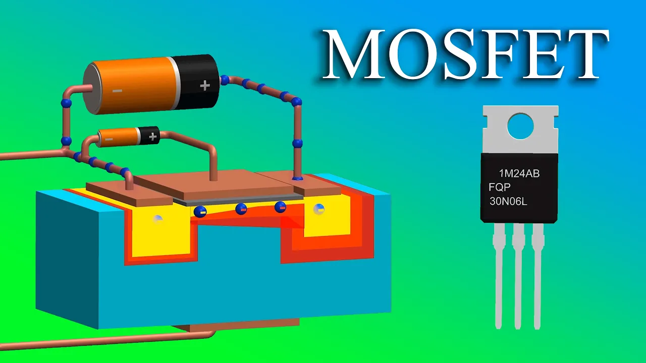
MOSFET Working Principle: Semiconductor Physics Explained
@ExplorerStuff
1.5M views•2020-12-04

30:32
Ultrasonic Transducers: Resonant Frequency Measurement and Horn Design
@imajeenyus42
229.9K views•2017-02-22

54:16
Polymer Environmental Degradation: Mechanisms & Stabilization
@iit
1.8K views•2012-07-10
33:39
How a Student's Question Saved a NYC Skyscraper from Collapse
@veritasium
22.8M views•2025-04-26
Related Study Plans & Knowledge Roadmaps
Structured learning paths in Engineering
engineering
Building Acoustic Levitators: Physics & Arduino
01The Physics of Sound and Standing Waves
02Piezoelectric Transducers and H-Bridge Drivers
03Arduino Programming: Generating 40 kHz Signals
+ 2 more learning modules
14h5 modules
Explore Roadmap
engineering
Building Peltier Cloud Chambers: Particle Tracks
01Cosmic Rays & Cloud Chamber Physics
02Thermoelectric Cooling (TEC) Fundamentals
03Custom Liquid-Cooling Loop Design
+ 2 more learning modules
18h5 modules
Explore Roadmap
engineering
Yagi-Uda Antennas: Modeling, Build & VNA Test
01Introduction to RF and Antenna Fundamentals
02Yagi-Uda Antenna Design Principles
03Antenna Modeling and Simulation in 4NEC2
+ 2 more learning modules
18h5 modules
Explore Roadmap
engineering
ECG Monitor Design: Op-Amps, Filters & Noise
01Electronics & Breadboard Basics
02Op-Amps and Instrumentation Amplifiers
03Bioelectricity and ECG Fundamentals
+ 2 more learning modules
18h5 modules
Explore Roadmap