This video demonstrates the complete process of fabricating PDMS microfluidic devices through soft lithography, which involves creating a master mold by patterning SU-8 photoresist on a silicon wafer using UV lithography, then casting PDMS (prepolymer:curing agent ratio of 10:1) onto the mold, curing it, punching inlet/outlet holes, treating the PDMS surface with oxygen plasma to make it hydrophilic, and finally bonding it to a glass substrate to create a sealed microfluidic device.
PDMS Microfluidic Device Fabrication: SU-8 Soft Lithography Tutorial
Added:Deep Dive
Basic principles of photolithography, including the difference between positive and negative photoresists (like SU-8), UV exposure, and photomasks.

Mod-02 Lec-13 Lithography - I
29.3K
Photolithography follows a systematic four-step process: substrate preparation, film deposition, photoresist coating, and pattern transfer. The fundamental mechanism involves projecting light through a patterned mask onto a light-sensitive photoresist layer, causing chemical changes that enable selective removal. Photoresist composition includes resin (binder), sensitizer (light-activated compound), solvent (controls viscosity), and adhesion promoter. Photoresists are classified as positive (exposed areas dissolve) or negative (exposed areas polymerize). SU8 represents a commercially successful negative epoxy photoresist operating in near-UV range, valued for its high aspect ratio capabilities and mechanical stability in demanding applications.
Click to watch →
Lec 35: Lithography & Pattern transfer
936
Lithography applies patterns onto substrates using light through photomasks. Photoresist composition includes photoactive compounds, resin, and solvents applied via spin coating. Exposure to UV light (mercury vapor lamps at 365nm I-line, excimer lasers at 248nm/193nm) changes solubility: positive resists dissolve after exposure, negative resists polymerize and resist dissolution. Resolution improves with shorter wavelengths. Photomasks are chromium-patterned glass substrates created via standard photolithography. Uniform illumination prevents speckles that degrade pattern quality. Photoresist development involves calculating exposure dose (50-500 mJ/cm²) and utilizing nonlinear solubility dynamic range for excellent contrast.
Click to watch →

Mod-06 Lec-26 Photoresist and application methods,UV exposure and developing
2K
Photoresist is an organic polymer that changes chemical structure when exposed to UV light, enabling image transfer onto PCBs. Two main types exist: positive resist (exposed areas become soluble in developer) and negative resist (exposed areas become insoluble). The choice between them depends on whether circuit areas need protection or removal. For fine-line PCBs (2-4 mil lines), excellent photoresist with good aspect ratio at low thicknesses is essential. The complete photolithography process involves: (1) applying photoresist, (2) tacky curing, (3) UV exposure through a mask, (4) developing to reveal the circuit pattern, and (5) hard baking before etching. Curing steps ensure the resist resists chemical attack during subsequent processes.
Click to watch →

Techniques in Mechanobiology: Microfabrication | Cell Shape Control & Traction Force Microscopy
757
Photolithography is a microfabrication process for selectively removing thin film or substrate material. Light transfers geometric patterns from photo masks to photoresist. The process workflow includes: spin coating for uniform photoresist application (higher RPM produces thinner layers), soft baking, mask alignment for light exposure through photo masks, and development. Two photoresist types exist: positive (e.g., Shipley 1813) becomes more soluble after exposure, while negative (e.g., SU-8) becomes less soluble. Photomasks are opaque plates with holes allowing light passage, made from chrome, glass, or transparencies.
Click to watch →
Introduction to fabrication technology Contd…
6K
Photoresist is a photosensitive polymer used in photolithography to transfer design patterns onto semiconductor wafers; it changes its solubility when exposed to UV light, with positive photoresist protecting unexposed areas and negative photoresist protecting exposed areas. The complete photolithography process includes wafer cleaning, dehydration (pre-bake), HMDS primer coating, spin coating, soft bake (90°C for 1 minute), mask alignment and UV exposure, development, hard bake (120°C for 1 minute), and inspection. Photoresist is spin-coated using centrifugal force where coating thickness decreases with higher RPM and longer spin time. Soft baking improves adhesion, uniformity, hydrophobic resistance, and light absorption characteristics. Masks come in bright field (opaque pattern on transparent background) and dark field (transparent pattern on opaque background) types, which determine how patterns are transferred depending on whether positive or negative photoresist is used.
Click to watch →
Deep Dive
Chemical and physical properties of Polydimethylsiloxane (PDMS) as an elastomer, including its gas permeability and optical transparency.
HE 218 - Lecture 2 - Introduction to microfabrication
656
Polydimethylsiloxane (PDMS) is a silicone-based polymer with a unique silicon-oxygen backbone instead of carbon-carbon bonds. As an elastomer, it has rubber-like flexibility with limited chemical stability. Unlike glass and silicon, PDMS is porous, allowing air to pass through its structure (though permeability is very low). It is transparent and has good thermal stability up to approximately 150-200°C. The main advantage of PDMS is its suitability for soft lithography prototyping, enabling rapid device replication outside cleanroom environments at much lower cost and faster turnaround times compared to silicon and glass fabrication.
Click to watch →

Lecture video 2 _17ME745_Module5 _Other Polmers and MICROFLUID Introduction _ Dr C Anil Kumar
131
Polydimethylsiloxane (PDMS) is an elastomer material that can sustain large deformation and recover its shape after force application. It has major applications in silicon-based elastomer family for sensors and actuators. Key properties include transparency, electrical insulation, mechanical elasticity, gas permeability, and biocompatibility. PDMS is widely used in microfluidics and sensing applications due to these characteristics.
Click to watch →
AFMS Conversations in Fluids - March 2022 - Dr Himali Somaweera (Gustavus Adolphus College)
105
Polydimethylsiloxane (PDMS) is a widely used material in microfluidic device fabrication due to its favorable properties. Key characteristics include optical transparency for visual monitoring, biocompatibility for cell culture applications, gas permeability that allows oxygen diffusion to support cell survival, chemical inertness toward many organic solvents, elastomeric properties enabling reversible deformation, and surface modifiability (can be made hydrophilic). These properties make PDMS ideal for creating microfluidic chips for biological experiments.
Click to watch →
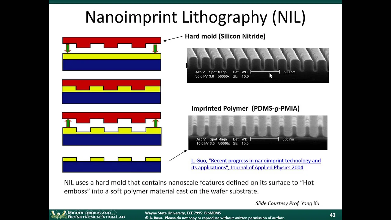
BioMEMS Module 3C: BioMEMS Fabrication
2.9K
PDMS is inexpensive, elastic, optically transparent with low autofluorescence, and biocompatible. Its surface is naturally hydrophobic but can be made temporarily hydrophilic with oxygen plasma treatment. PDMS swells when exposed to certain acids and can self-seal by conformal contact. It has high permeability to gases and fluids, which is beneficial for cell culture applications.
Click to watch →

Lec 17: Synthetic Biomedical Polymers-1 | Polymeric Biomaterials
125
Silicones are inorganic polymers with silicon-oxygen backbone and pendant organic groups. The Si-O bond polarity and low rotation energy provide exceptional stability and flexibility. Properties range from fluids to elastomers to gels depending on molar mass, cross-linking degree, and pendant groups. PDMS has very low glass transition temperature and high free volume, providing excellent elastomeric behavior and gas permeability. However, hydrophobic methyl groups make PDMS prone to protein adsorption and fibrous capsule formation. Silicone elastomers are 3D covalently cross-linked networks with fillers for reinforcement. Silicone gels are lightly cross-linked networks between fluids and elastomers. Applications include extracorporeal equipment (dialysis, blood oxygenators), catheters, drains, shunts, and reconstructive surgery.
Click to watch →
Deep Dive
Standard cleanroom safety protocols, including particulate control and the safe handling of hazardous fabrication chemicals and solvents.

MTTC Cleanroom Safety Lecture 2019
1.6K
Cleanroom safety requires understanding particle contamination control (ISO Class 6/Class 1000 cleanrooms limit particles to 1,000 per cubic foot), proper gowning procedures (hairnet, face shield, beard bag, booties, smock, gloves, safety glasses), emergency protocols (evacuation to assembly points, calling UNM police for emergencies), chemical safety (SDS review, proper PPE including triple tria gloves and acid aprons, never submerging body parts in chemicals), and waste disposal (separate containers for corrosives, flammables, sharps, and regular waste).
Click to watch →
Lec 3: Fabrication Process - II
2K
This extensive section covers clean room operations essential for microfabrication. Topics include: (1) Wafer contamination sources—organic (skin oils, body fluids), metallic (sodium, potassium, heavy metals), native oxide (<10nm), and micro roughness requiring thorough cleaning; (2) Clean room classification by particle concentration: Class 1 (1 particle/cubic ft), Class 10, Class 100, etc., with HEPA filtration and controlled environmental parameters (temperature, humidity, sound, lighting); (3) Personnel protocols: gowning sequence (gloves → gown → hairnet → face mask), prohibited items (fur, jewelry), prohibited activities (eating, mobile phones), and communication restrictions; (4) Wet bench safety: acid-specific gloves, HF handling in Teflon containers, fume hood requirements, proper chemical mixing (acid to water), MSDS consultation; (5) Emergency response: spill procedures (flush skin immediately), disposal protocols, and first aid availability.
Click to watch →

MTTC Safety Lecture Part 1
742
Clean rooms require comprehensive safety protocols including yellow lighting (filtered blue/green light to prevent wafer exposure), emergency information sheets at exits, Patron and Halon fire extinguishers for electrical fires, and CO2 systems for solvent hoods. Humans are the biggest contamination source, shedding thousands of particles per second. Clean rooms are classified by particle count standards: Class 1,000 allows up to 1,000 half-micron particles per cubic foot, while Class 10 allows only 10 particles. Semiconductor devices are extremely small: transistor gates are 2 microns or smaller, while gear teeth in devices are 8 microns (red blood cell size). A single particle landing on a transistor during processing can short out the device. Clean room rules prohibit makeup, hair gel, cologne, and smoking (20-minute waiting period required). PPE includes hair nets, shoe covers, face masks, smocks, and chemical gloves. Contact lenses are prohibited because chemical fumes can collect on or under lenses, potentially fusing to the cornea. Proper gowning order is: shoe covers, hair net, face cover, gloves, smock, and safety glasses.
Click to watch →
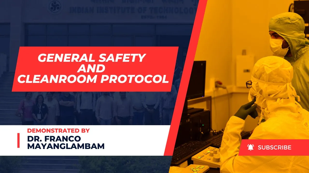
General Safety and Cleanroom Protocol | Dr. Franco Mayanglambam | Centre for Nanotechnology | IITG
590
Cleanrooms are controlled environments that minimize airborne particles to enable precision manufacturing and R&D activities, with Class 100 and Class 1,000 cleanrooms housing lithography and deposition equipment respectively; human personnel are the primary contamination source, releasing millions of particles daily, so strict protocols including pre-entry preparation (no food, cosmetics, jewelry, or personal items), proper gowning procedures (hairnet, coverall, booties, gloves), and adherence to safety guidelines (no eating/drinking, proper chemical handling, waste disposal protocols) are essential to maintain sterile conditions and prevent contamination of sensitive processes.
Click to watch →

National Nanofabrication Centre at CeNSE, IISc Bangalore
1.1K
Clean rooms are precisely controlled environments where particle count, temperature, and humidity are strictly maintained to prevent contamination during semiconductor fabrication. The National Nanofabrication Centre (NNFC) at IISc Bangalore operates Class 100 and Class 1000 clean rooms, with Class 100 reserved for highly sensitive lithography areas. Contamination is categorized into three types: airborne/molecular (from outgassing, oils, and chemicals), surface contamination (fingerprints, oils, skin products), and particulate contamination (from clothing fibers, skin scales, and materials). Humans contribute approximately 75% of all particles, making proper gowning procedures essential—using face masks, hair nets, polyester bunny suits, booties, and gloves. Emergency protocols include using lined phones to contact Building Maintenance System (BMS) at 115, following buddy systems, and immediate evacuation during gas or fire alarms. Wet bench areas require additional PPE including chemical-resistant gloves (nitrile for general chemicals, epilon for HF), face shields, and aprons. Hazardous chemicals like HF and BOE require special handling due to their corrosive nature and potential to affect bone calcium and central nervous system.
Click to watch →
Deep Dive
Fundamental concepts of microfluidics, particularly laminar flow behavior and scaling effects at the micron level.
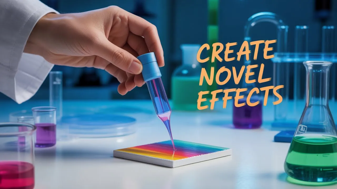
Scientists Just Turned Fluid Dynamics Into Fine Art
106
Micrfluidics manipulates fluids at the microscale (microliter to picoliter range) using channels thinner than a human hair (10-500 micrometers). At this scale, surface forces dominate over gravity, and Reynolds numbers typically fall below 1, resulting in laminar flow where fluids move in parallel layers with minimal mixing. This enables precise control of fluid behavior that differs fundamentally from macroscopic fluid dynamics.
Click to watch →

Microfluidics and Lab-on-a-Chip: Progress and Challenges
268.6K
At micro-scale dimensions (about one micrometer), liquid flows tend to be laminar rather than turbulent. In laminar flow, fluid streams move parallel to each other without mixing between them. When two fluid streams join together in a microchannel, they end up going side by side rather than mixing immediately. This predictability makes microfluidic interactions very reliable and controllable.
Click to watch →

COMSOL's Hands-on Workshop on Microfluidic Devices @ NNIN/C, UMich
46.3K
Microfluidics exploits size reduction effects: volume scales with L³, reducing reagent consumption; viscous/inertial forces decrease, promoting laminar flow; Laplace pressure increases, making surface tension critical; diffusion times decrease, requiring active mixing; electric fields strengthen, enhancing electrokinetic effects. Five pumping mechanisms exist: capillary-driven (hydrophilic/hydrophobic surfaces), pressure-driven (pumps), centrifugal (rotating structures), electrokinetic (electric fields), and droplet-driven (surface tension effects). Each mechanism offers advantages for specific applications, from medical diagnostics to chemical synthesis. Understanding these principles enables rational design of microfluidic devices for various analytical and synthetic purposes.
Click to watch →

première partie résumé cours intensification
432
Microfluidics manipulates small fluid volumes in channels ranging from tens to hundreds of micrometers. The fundamental principle is that reducing system dimensions dramatically increases the surface-to-volume ratio, which directly improves heat and mass transfer between phases. At the microscale, surface phenomena (diffusion, surface tension, viscosity) become dominant over bulk phenomena (inertial effects). The Reynolds number (Re = ρvD/μ) determines flow regime, with microfluidic systems typically showing Re values of 0.001 to 0.5, indicating laminar flow where viscous forces dominate. In laminar flow, mixing occurs primarily through molecular diffusion rather than convective turbulence, with a parabolic velocity profile (v = Vmax(1 - r²/R²)). The pressure drop in laminar flow is directly proportional to flow rate (ΔP ∝ Q), enabling precise control over flow rates in microfluidic systems.
Click to watch →
Spaghettis boulettes & Microfluidique avec Stéphanie Descroix
255
Microfluidics is the study of fluid flow through channels at micrometer scales (approximately the diameter of a hair, about 100 micrometers). At this scale, fluids behave differently than in larger systems—unlike rivers where turbulence creates mixing, microfluidic systems show laminar flow where different liquids flow side by side without mixing. Gravity becomes negligible at this scale, and the physics has unique characteristics that make it valuable for scientific applications. This field combines biology, chemistry, physics, and engineering, with applications extending to energy research and nanotechnology.
Click to watch →
Prerequisite Knowledge
- Concept 01Basic principles of photolithography, including the difference between positive and negative photoresists (like SU-8), UV exposure, and photomasks.
- Concept 02Chemical and physical properties of Polydimethylsiloxane (PDMS) as an elastomer, including its gas permeability and optical transparency.
- Concept 03Standard cleanroom safety protocols, including particulate control and the safe handling of hazardous fabrication chemicals and solvents.
- Concept 04Fundamental concepts of microfluidics, particularly laminar flow behavior and scaling effects at the micron level.
Subsequent Learning
- Step 01Metrology and characterization techniques to verify channel dimensions, such as optical profilometry and Scanning Electron Microscopy (SEM).
- Step 02Advanced bonding and surface modification techniques, such as optimizing oxygen plasma treatment parameters for permanent PDMS-glass sealing.
- Step 03Integration of fluidic control hardware, including pneumatic valves, syringe pumps, and microscopic imaging setups to run active experiments.
- Step 04Real-world biomedical and chemical applications, such as Organ-on-a-Chip platforms, droplet microfluidics, and lab-on-a-chip diagnostics.
Mold Creation
UV Patterning
Developing Mold
PDMS Casting
Bonding Device
Mold Creation
0:05Playing Section
- 1
Clean silicon wafer using Nano Strip to prepare substrate.
- 2
Fabricate SU-8 mold via photolithography process.
- 3
Employ spin coating and soft baking for layer formation.
Thermoplastic and 3D-Printed Microfluidics: Moving Beyond PDMS and Cleanroom Constraints
While SU-8 soft lithography with PDMS is the academic standard for microfluidics, it faces critical limitations regarding scalability, material properties, and cost. PDMS is highly porous and prone to absorbing small hydrophobic molecules, which can compromise drug-screening assays. Furthermore, PDMS fabrication is labor-intensive and unsuitable for industrial-scale manufacturing. To address these drawbacks, the field is shifting toward alternative materials and cleanroom-free fabrication. Thermoplastics—such as Cyclic Olefin Copolymer (COP), Polymethyl Methacrylate (PMMA), and Polystyrene—are preferred for commercial applications because they are chemically inert, rigid, and compatible with high-volume injection molding. Additionally, rapid prototyping methods like high-resolution 3D printing and micro-milling completely bypass the expensive cleanroom infrastructure required for SU-8 photolithography, democratizing microfluidic development and accelerating commercial translation.
Deep Dive
Metrology and characterization techniques to verify channel dimensions, such as optical profilometry and Scanning Electron Microscopy (SEM).

Ben Tsai: Inspection and Metrology to Support the Quest for Perfection
16.7K
Critical Dimension (CD) and shape metrology requires different approaches based on application: CD-SEM remains used for discovery applications like OPC verification and line edge roughness characterization, while optical CD tools offer advantages for production process window expansion and control where precision matching is critical. For multiple patterning requiring measurement of sidewall angles and other parameters, only optical CD can provide comprehensive measurements since CD-SEM is limited to top-down measurements. Isolated feature measurement presents challenges because existing scatterometry CD tools become more sensitive to underlayer effects when feature density is low, requiring enhanced differential phase shift techniques and improved signal processing.
Click to watch →

Introduction to Optical Profilometry
8.1K
Optical profilometry is a non-contact, non-destructive surface metrology technique that uses Coherence Scanning Interferometry (also known as Scanning White-Light Interferometry) to measure surface properties such as roughness and topography by exploiting the wave properties of light, specifically phase and coherence; the technique works by splitting a light beam into reference and test paths, scanning the test path length, and detecting interference patterns to determine surface height at each pixel, with the Zero Optical Path Difference (ZOPD) indicating when the test and reference paths are equal, allowing for rapid data acquisition across large fields of view through image stitching.
Click to watch →

Lecture on Characterization Techniques by Dr. Fahmida Jabeen | IM GROUP OF RESEARCHERS
214
Characterization techniques verify material properties after development or modification. Optical light cannot image at micro/nano scales, requiring electron-based microscopy. Scanning Electron Microscopy (SEM) uses electrons to image surfaces, providing topography, composition, conductivity, and crystallinity information. Three detector types exist: secondary electrons (surface detail), backscattered electrons (compositional contrast), and Energy Dispersive X-ray Spectroscopy (EDS) for elemental analysis. Each serves distinct research objectives.
Click to watch →
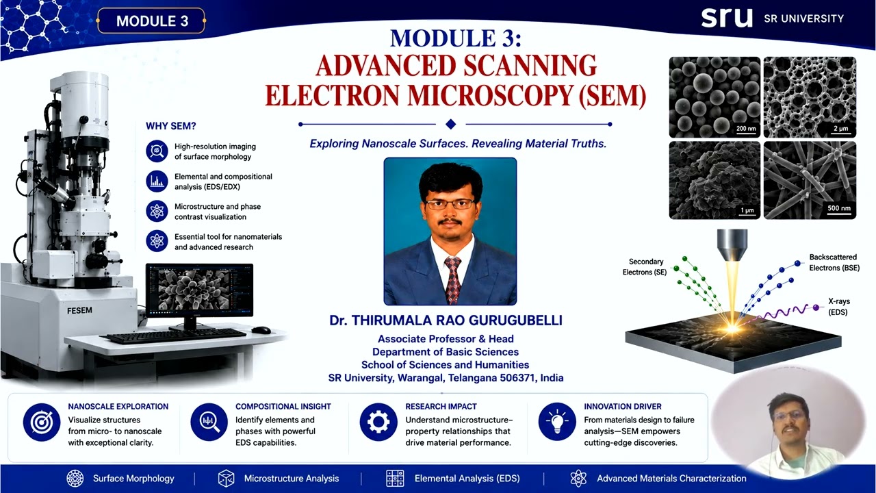
Scanning Electron Microscope (SEM) Part 1
139
Scanning Electron Microscopy (SEM) is an advanced characterization technique that uses a focused electron beam to generate high-resolution images of material surfaces by detecting secondary electrons (for topographic contrast), backscattered electrons (for compositional contrast), and characteristic X-rays (for elemental analysis via EDS), overcoming the resolution limitations of optical microscopes at the nanoscale.
Click to watch →
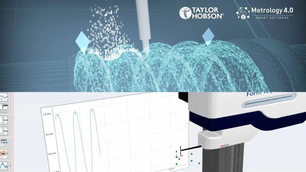
Surface Finish | Contour | 3D | Diameter Measurement | PGI NOVUS Product Launch
5.3K
Optical profilometry is a non-contact measurement technology that uses light to capture and analyze surface topography, enabling precise measurement of surface finish, contour, 3D features, and diameter across various environments from shop floor to laboratory.
Click to watch →
Deep Dive
Advanced bonding and surface modification techniques, such as optimizing oxygen plasma treatment parameters for permanent PDMS-glass sealing.
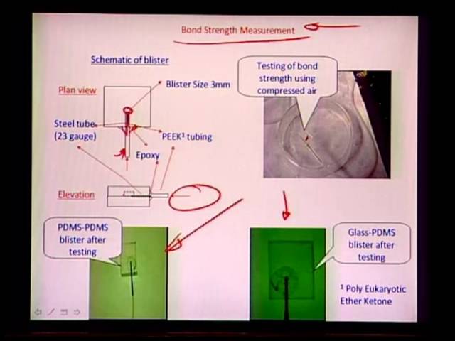
Mod-01 Lec-38 Lecture-38
356
Oxygen plasma converts hydrophobic PDMS surfaces (contact angle ~108°) to hydroxylated states through UV excitation and radical attack. The five-step chemical mechanism generates Si-OH groups that enable irreversible siloxane bonding between surfaces. Optimal bonding occurs when contact angle falls below 10°, correlating with maximum hydroxyl group density. High-pressure low-power conditions minimize substrate damage while achieving effective surface activation.
Click to watch →
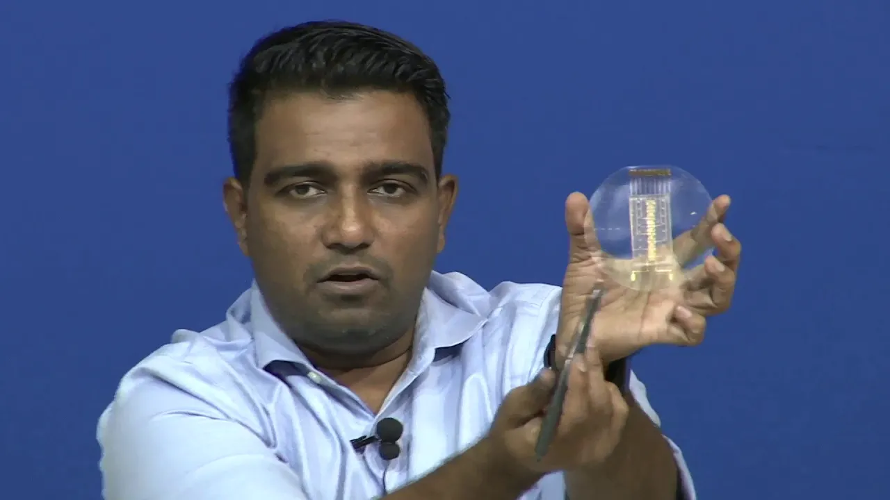
mod08lec27
1.2K
This section covers the final stages of microfluidic device fabrication and assembly. The process involves: (1) pouring PDMS onto the SU-8 mold, (2) curing at 115°C for 15 minutes, (3) peeling off cured PDMS to reveal channels, and (4) oxygen plasma treatment (800 watts, 10 mTorr) to functionalize surfaces for bonding. The plasma treatment creates reactive surfaces that allow permanent bonding between PDMS and the glass substrate containing the microheater and electrodes. To enable drug loading and cell introduction, holes are created in the PDMS using biopsy needles to serve as inlets and outlets. These access points allow researchers to introduce cancer cells (loaded with Matrigel for extracellular matrix replication) into shorter channels and flow different drugs through longer channels. Without these access points, the system would be sealed and unable to receive biological samples and therapeutic agents needed for drug screening experiments.
Click to watch →

Microfluidics by soft lithography - Part 9 - Bonding
847
Atmospheric plasma bonding is a technique used to permanently attach PDMS microfluidic chips to glass substrates by exposing both surfaces to plasma, which creates covalent silicon-oxygen-silicon bonds; the process requires evacuating the chamber, introducing controlled gas flow, generating plasma for approximately 15 seconds, and then carefully aligning and pressing the PDMS chip onto the substrate to form a permanent bond.
Click to watch →
MechanoBio 101 for Teachers: Intro Soft Lithography and Microcontact Printing By Kapish Gupta
277
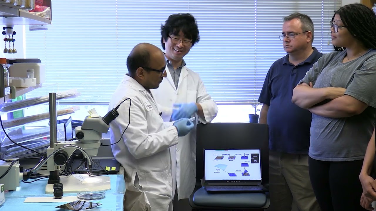
PDMS naturally exhibits hydrophobic properties, causing liquids to bead up on its surface. However, for many biological applications, hydrophilic surfaces are needed to ensure proper protein attachment and cell adhesion. Plasma treatment converts PDMS surfaces to hydrophilic by breaking surface bonds and reacting them with oxygen molecules. The degree of hydrophilicity depends on treatment parameters including oxygen flow rate and exposure duration. This surface modification is essential for successful microcontact printing of biological molecules.
Click to watch →
PDMS Bonding (Microfluidic Devices) with Harrick Plasma
6.6K
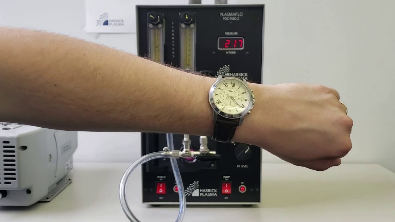
Plasma treatment activates PDMS surfaces by introducing reactive silanol groups, enabling covalent bonding between PDMS components or PDMS-glass interfaces; the process involves evacuating the chamber, introducing controlled gas flow (air or oxygen), applying RF power to generate plasma, treating for approximately 50 seconds, and immediately pressing surfaces together for 30 seconds, with optimal bonding occurring within 15-60 minutes post-treatment and optional thermal annealing at 80-100°C for enhanced bond strength.
Click to watch →
Deep Dive
Integration of fluidic control hardware, including pneumatic valves, syringe pumps, and microscopic imaging setups to run active experiments.
Building a lab-on-a-chip
10.2K
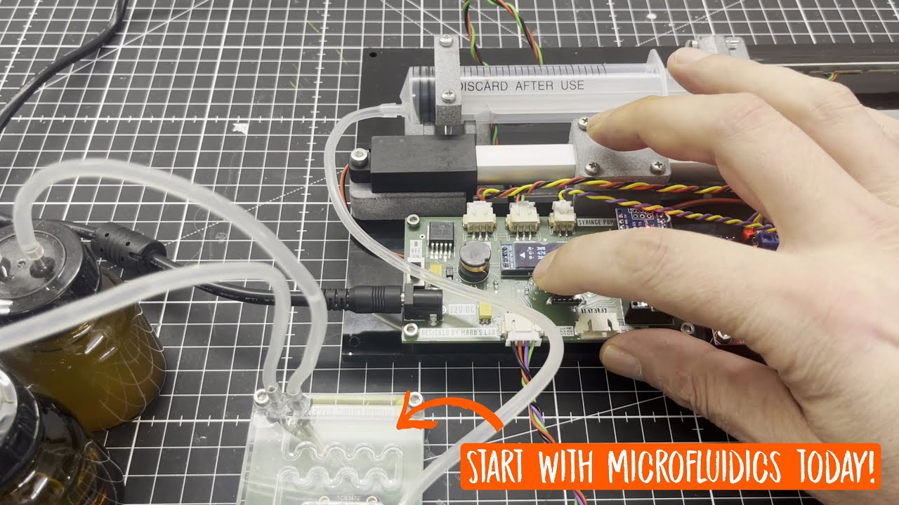
Complete microfluidic systems require integrated hardware components including color sensors, sampling bottles, and syringe pumps. TCS 34725 RGB color sensors with infrared filters detect chemical reactions through color changes, communicating via I²C protocol. Sampling bottles are constructed from 50ml amber glass bottles with drilled caps, stainless steel tube inserts, and silicone seals connected to aquarium one-way valves. Syringe pumps use 12V linear actuators with 100mm stroke, sliding potentiometers for feedback, and 3D-printed mechanical structures. L298N motor drivers provide cost-effective control for these pump mechanisms.
Click to watch →

Microfluidic Flow Control
274
A microfluidic flow control system consists of three layers: a control layer with valves, a PDMS layer in between, and a flow layer, which are assembled by cleaning components, aligning schematics, clamping with eight clamps, and placing in a desiccator; the system uses an RC servo motor controlled by an FPGA to actuate valves, while a syringe pump delivers fluids to the flow layer, enabling precise control of fluid movement in microfluidic experiments.
Click to watch →
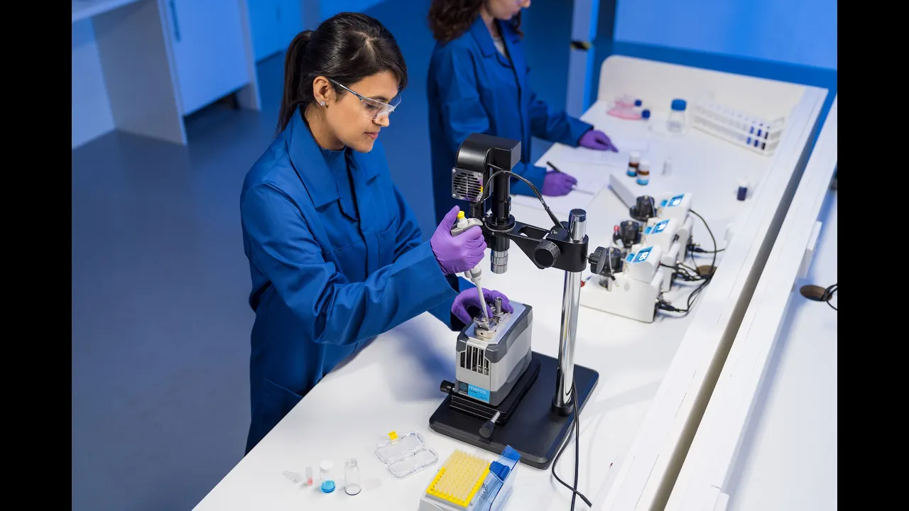
Product demo - uEncapsulator System
412
The system uses three P-pumps with glass scintillation vials holding liquids. Two pumps contain driver fluid (aqueous or oil-based, such as fluorinated oil), while the third holds the continuous phase (typically Fluosurf for biological compatibility). Each pump holds up to 30 ml. Dip tubing must be immersed before operation. Flow sensors measure flow rates using thermal technology. Inline valves enable user control. The reservoir chip holds cargo (cells, beads, buffers) at 100 μL per channel, loaded via pipette. The droplet microfluidic chip interfaces with the reservoir chip through a linear connector, enabling real-time observation via high-speed camera and microscope.
Click to watch →

Programmable Micofluidics
13K
The valve is the fundamental primitive, built with two layers (control and flow) using photoresist and plastic molding. Multiplexers select flow lines by blocking alternatives, requiring log(n) control lines. Mixers combine fluids using rotary systems with peristaltic pumps. Latches catch samples at specific locations for precise alignment. Cell traps use U-shaped sieves to immobilize cells while allowing fluid flow through. These primitives enable complex biological experiments including cell culture, metabolite extraction, and real-time feedback control.
Click to watch →
Webinar 1: Setting up a microfluidic system
1.4K
A complete microfluidic system integrates multiple specialized hardware components working in concert. The central control unit (MP multi-board) coordinates pump drivers (low/high performance variants), valve drivers controlling shape memory alloy actuators, and sensor interfaces for flow and pressure measurement. Fluidic components include pulsating micropumps requiring flow dampers for stabilization, Y-connectors for pressure tapping, and two-way valves for fluid-gas separation. Proper orientation during component connection is critical, particularly for thin flex cables and valve drivers. The system architecture enables routing fluids through microfluidic chips while maintaining precise control over flow rates, pressures, and fluid phases.
Click to watch →
Deep Dive
Real-world biomedical and chemical applications, such as Organ-on-a-Chip platforms, droplet microfluidics, and lab-on-a-chip diagnostics.
Organ-on-chip 101 – Your Introduction to the Future of Biomedical Research
163
Organ-on-a-chip technology represents a transformative approach to biomedical research, addressing limitations of traditional 2D cultures and animal models. The technology provides controlled experimental conditions with physiological complexity, including 3D architecture, dynamic mechanical cues, oxygen gradients, and immune cell integration. Real-world applications demonstrate its value: lung-on-chip models reveal co-infection mechanisms and enable antifungal drug testing; gut-on-chip models capture Candida albicans microcolony formation and drug resistance; liver-on-chip models successfully predicted trovafloxacin hepatotoxicity; cancer-on-chip models enable immunotherapy testing with circulating immune cells. The system supports multiple assay types including barrier permeability, live imaging, and enzymatic activity measurements.
Click to watch →

NanoBiotech Laboratory, Dept of Bio and Brain Eng, KAIST (바이오및뇌공학과 나노바이오공학 연구실)
247
This video introduces microfluidic lab-on-a-chip technology developed at KAIST, which integrates biological sample pre-processing and detection into miniature devices for life science, chemistry, medicine, and environmental applications. Key innovations include point-of-need testing (Poc) for immediate diagnostics, finger-force microfluidic control eliminating external equipment, and digital PCR systems for genetic analysis. The research extends to organ-on-a-chip technology using 3D cell culture to model vascular occlusion, intestinal inflammation, and hepatic metabolism. Spheroid array technology enables high-throughput analysis of cellular responses. These platforms aim to replace animal testing, accelerate drug development by evaluating safety and efficacy, and provide more accurate human-relevant disease models for pharmaceutical research.
Click to watch →

Microfluidics _Huh, 2020
670
This comprehensive section covers the foundational concepts of microfluidics and their application in creating advanced organ-on-a-chip systems. Microfluidics is defined as manipulating small fluid volumes (tens to 100 micrometers) with precise control, enabling capabilities impossible with traditional lab techniques. Key applications include droplet formation for high-throughput reactions, laminar flow patterning, and multi-layer soft lithography. The field experienced exponential growth post-1990s, with three main biomedical applications: diagnostics for resource-limited settings, rapid biofluid analysis, and physiological process modeling. Organ-on-a-chip technology uses microengineering to create simplified yet physiologically relevant models following a reductionist approach: identifying functional units (alveoli, liver lobules, nephrons), determining structural features (three-layer barriers), and designing microfluidic systems to replicate them. Lung-on-a-chip examples demonstrate two-chamber designs with flexible PDMS membranes, epithelial cells under air, vascular cells with flowing media, and cyclic vacuum creating mechanical stretching mimicking breathing. Multi-tissue interactions enable modeling complex physiological processes like immune cell recruitment during lung infections. Disease modeling applications include smoking lung disease platforms showing fibrotic responses, vascularized tumor models for cancer immunotherapy testing, and asthma models using compressible chambers to study mechanical force effects on tissue pathology.
Click to watch →
Капельная микрофлюидика
2.1K
Droplet microfluidics is a technology that generates uniform microdroplets (20+ micrometers) at frequencies of several thousand per second by forcing two immiscible liquids through intersecting microchannels, enabling rapid biochemical reactions in individual droplets that can replace traditional multi-well plates. This technology accelerates drug development, improves analytical precision, and enables single-cell analysis by encapsulating cells or DNA molecules in isolated droplets, where reactions can be performed in parallel with high throughput and reduced reagent consumption.
Click to watch →

Organs-on-Chips: New science and standards for implementation (Sept 2021)
476
Organ-on-chip technology uses microfluidic systems to create microphysiological environments mimicking in vivo conditions. Key advantages include replicating shear stress effects on cells, removing harmful metabolites through continuous flow, and creating stable models for subchronic studies. Four major commercial platforms exist: Emulate's PDMS-based system with mechanical stretching capabilities, TissUUart's circulatory chip with interconnected organ compartments, OrganBlade's rocking-motion system with bi-directional flow and gel barriers, and Micronet's glass-based system offering inert material advantages for hydrophobic compounds. These systems serve diverse applications in food safety, cosmetics, pharmaceuticals, and toxicological research including PBK modeling, transport studies, disease modeling, and mechanistic research on cell interactions and vascularization.
Click to watch →
Mold Creation
UV Patterning
Developing Mold
PDMS Casting
Bonding Device
Mold Creation
0:05- 1
Clean silicon wafer using Nano Strip to prepare substrate.
- 2
Fabricate SU-8 mold via photolithography process.
- 3
Employ spin coating and soft baking for layer formation.
Thermoplastic and 3D-Printed Microfluidics: Moving Beyond PDMS and Cleanroom Constraints
While SU-8 soft lithography with PDMS is the academic standard for microfluidics, it faces critical limitations regarding scalability, material properties, and cost. PDMS is highly porous and prone to absorbing small hydrophobic molecules, which can compromise drug-screening assays. Furthermore, PDMS fabrication is labor-intensive and unsuitable for industrial-scale manufacturing. To address these drawbacks, the field is shifting toward alternative materials and cleanroom-free fabrication. Thermoplastics—such as Cyclic Olefin Copolymer (COP), Polymethyl Methacrylate (PMMA), and Polystyrene—are preferred for commercial applications because they are chemically inert, rigid, and compatible with high-volume injection molding. Additionally, rapid prototyping methods like high-resolution 3D printing and micro-milling completely bypass the expensive cleanroom infrastructure required for SU-8 photolithography, democratizing microfluidic development and accelerating commercial translation.
Basic principles of photolithography, including the difference between positive and negative photoresists (like SU-8), UV exposure, and photomasks.
Chemical and physical properties of Polydimethylsiloxane (PDMS) as an elastomer, including its gas permeability and optical transparency.
Standard cleanroom safety protocols, including particulate control and the safe handling of hazardous fabrication chemicals and solvents.
Fundamental concepts of microfluidics, particularly laminar flow behavior and scaling effects at the micron level.
Metrology and characterization techniques to verify channel dimensions, such as optical profilometry and Scanning Electron Microscopy (SEM).
Advanced bonding and surface modification techniques, such as optimizing oxygen plasma treatment parameters for permanent PDMS-glass sealing.
Integration of fluidic control hardware, including pneumatic valves, syringe pumps, and microscopic imaging setups to run active experiments.
Real-world biomedical and chemical applications, such as Organ-on-a-Chip platforms, droplet microfluidics, and lab-on-a-chip diagnostics.
66.9K views698likes10:44@microfluidicsandmultiphase8434Original Release: 2015-05-18
hello everyone my name is lelu I'm in the clean room of bampton University today I'm going to show you how to make a pdms microtic device using software theography the first step is to create isolated mode on Silicon wafer and we first clean silicon wafer using Nano Street [Music] [Music] [Music] put your okay the next step is to spin coat a thin layer of negative photo resist su8 onto the clean silicon wafer [Music] [Music] so the next step is to sof bake the wafer at two temperatures 65 and 90° C so in preparation for this process we developed this photo mask of our Channel design previously now we want to use this photo mask with this mask aligner to pattern the propelled photo released layer [Music] so after UV patterning we conduct a post fake process at two steps 65 and 19° C after the poster B process we will develop this photo resist by immersing it in the sua development her [Music] [Music] [Music] having finished su8 mode now we are in the transport science core of bampton University to complete the second part of the soft lithography process we will cast a pdms onto the S Mode the ustomer is a mixture of pdms prepolymer and curing agent at a weight ratio of 10 to1 [Music] [Music] [Music] [Music] now the pdms is fully cured we can peel it off from the mold cut it into pieces and punch the Hol for channel inlets and outlets now we have this propelled pdms piece we removed any debris on surface using Scotch tape the next step is to treat its surface and a glass light hydrophilic using oxygen plasma then we Bond the two surfaces together to form a sealed microfluidic device is [Music] [Music]
Up Next

11:49
Multilayer Soft Lithography for Microfluidic Devices | Stanford Foundry
@emrear78
20.3K views•2012-01-11
30:32
Ultrasonic Transducers: Resonant Frequency Measurement and Horn Design
@imajeenyus42
229.9K views•2017-02-22

54:16
Polymer Environmental Degradation: Mechanisms & Stabilization
@iit
1.8K views•2012-07-10

33:39
How a Student's Question Saved a NYC Skyscraper from Collapse
@veritasium
22.8M views•2025-04-26
Related Study Plans & Knowledge Roadmaps
Structured learning paths in Engineering
engineering
Building Acoustic Levitators: Physics & Arduino
01The Physics of Sound and Standing Waves
02Piezoelectric Transducers and H-Bridge Drivers
03Arduino Programming: Generating 40 kHz Signals
+ 2 more learning modules
14h5 modules
Explore Roadmap
engineering
Building Peltier Cloud Chambers: Particle Tracks
01Cosmic Rays & Cloud Chamber Physics
02Thermoelectric Cooling (TEC) Fundamentals
03Custom Liquid-Cooling Loop Design
+ 2 more learning modules
18h5 modules
Explore Roadmap
engineering
Yagi-Uda Antennas: Modeling, Build & VNA Test
01Introduction to RF and Antenna Fundamentals
02Yagi-Uda Antenna Design Principles
03Antenna Modeling and Simulation in 4NEC2
+ 2 more learning modules
18h5 modules
Explore Roadmap
engineering
ECG Monitor Design: Op-Amps, Filters & Noise
01Electronics & Breadboard Basics
02Op-Amps and Instrumentation Amplifiers
03Bioelectricity and ECG Fundamentals
+ 2 more learning modules
18h5 modules
Explore Roadmap