Semiconductors: Band Theory to Transistors
Learning Goal: Understanding Semiconductor Physics: From Band Theory to the Mechanics of Modern Transistors. This curriculum bridges the gap between quantum mechanics, solid-state chemistry, and device engineering, helping you master how microscopic electron behaviors enable the global digital economy.
- Prerequisites: High school physics (basic electrostatics, electric potential, and atomic structure) and basic calculus.
- Estimated Total Study Time: 14 hours
Module 1: Quantum Foundations of Electronics
To understand how modern computer chips work, we must first abandon the view of electrons as tiny, solid billiard balls and examine their true quantum nature. This module establishes the quantum foundations of electronic structure, covering quantized energy levels, wave-particle duality, and the physical laws governing how electrons occupy states within isolated atoms before they coalesce into solids.
Recommended Videos
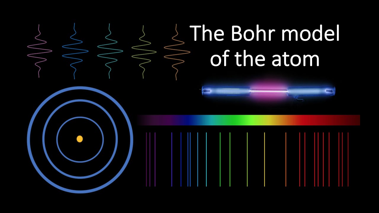
- Why this video: This video offers a rigorous historical and physical introduction to the Bohr model. It details how the quantization of angular momentum explains why electrons reside only in discrete, non-decaying orbits (shells), providing the ideal foundation for understanding discrete atomic energy levels.

- Why this video: Transitioning from the planetary Bohr model to the quantum mechanical model, this video explains electrons as 3D standing waves. It introduces Schrödinger's wave equations, atomic orbitals (s, p, d, f), and the fundamental rules (like the Pauli Exclusion Principle) that dictate orbital filling.

- Why this video: A short, highly visual demonstration of wave-particle duality. It explains why quantum entities behave as waves (producing interference patterns) until observed, establishing the conceptual mindset needed to grasp electron propagation in a crystal.
Knowledge Checkpoint
- Calculate or explain how the quantization of electron orbits prevents the electron from spiraling into the nucleus, resolving the core failure of classical Rutherfordian physics.
- Describe the physical significance of wave-particle duality and explain why electrons in atomic orbits are better represented as standing waves than orbiting point charges.
- Define the Pauli Exclusion Principle and explain how it prevents multiple electrons from occupying the exact same quantum state within an atom.
Module 2: Energy Band Theory in Solids
When isolated atoms come together to form a solid crystal lattice, their distinct quantum energy states interact. This module addresses a critical transition: how discrete atomic orbitals merge to form continuous valence and conduction bands, separated by forbidden band gaps. We will explore both qualitative molecular orbital theory and the mathematical foundations of electrons in periodic potentials.
Recommended Videos

- Why this video: This video directly bridges the gap identified in academic reviews: providing an intuitive, visual explanation of how atomic orbitals merge into continuous bands. Using Linear Combination of Atomic Orbitals (LCAO), it illustrates how overlapping orbital wavefunctions split into bonding (lower energy) and antibonding (higher energy) molecular states, scaling up to the massive energy bands of solid-state structures.

- Why this video: An exceptional lecture from MIT highlighting the mathematical and physical mechanics of wave function combination. It explains constructive and destructive interference of electronic wavefunctions, demonstrating how they form stable bonding zones and higher-energy antibonding zones.
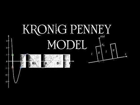
- Why this video: This video provides the mathematical foundation of band theory. It explains the Kronig-Penney model, which simplifies the crystal lattice into a 1D periodic rectangular potential barrier, showing how solving the Schrödinger equation in periodic boundaries naturally yields allowed energy bands and forbidden band gaps.
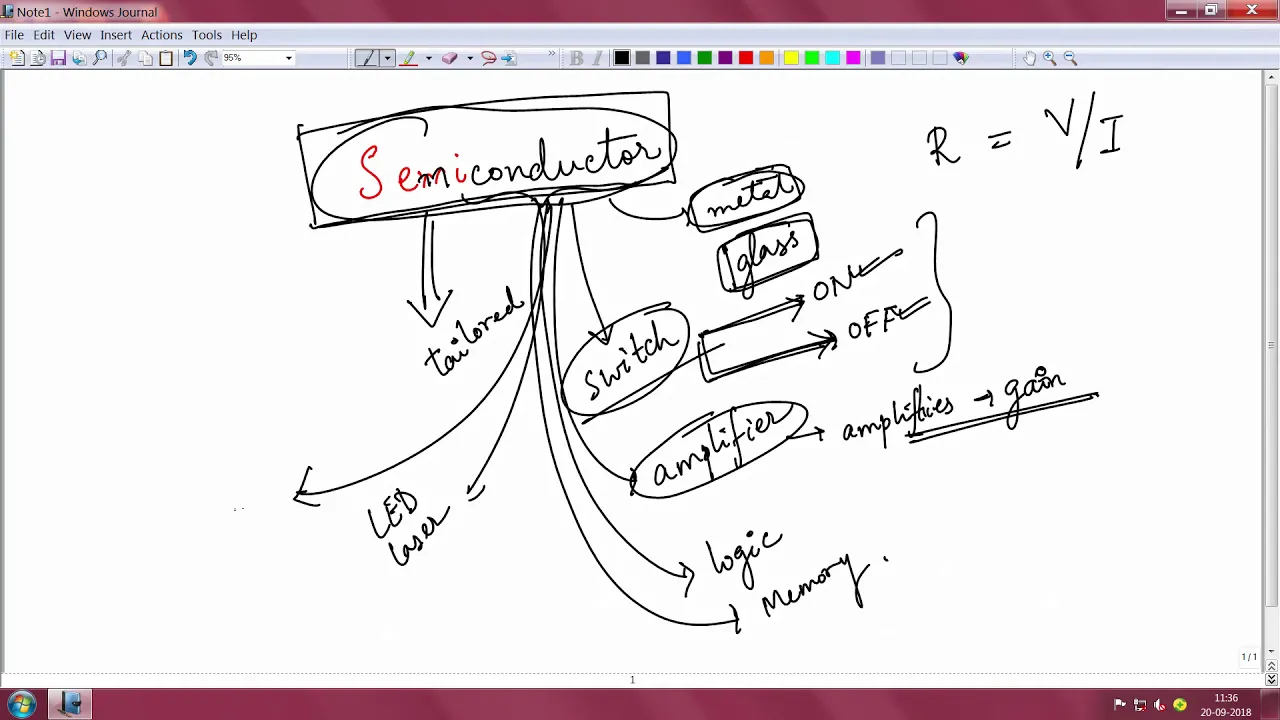
- Why this video: This video clearly defines the difference between conductors, insulators, and semiconductors based on the size of their band gap () and the temperature-dependent occupancy of the valence and conduction bands.
Knowledge Checkpoint
- Explain how the Linear Combination of Atomic Orbitals (LCAO) model accounts for the splitting of a single energy level into closely spaced states when atoms assemble into a lattice.
- Sketch an energy band diagram labeling the Valence Band, Conduction Band, Fermi Energy (), and Band Gap () for a metal, semiconductor, and insulator.
- Describe how the Kronig-Penney model uses a periodic potential to demonstrate the mathematical origin of forbidden energy states (band gaps).
Module 3: Doping and Charge Carriers
Pure (intrinsic) semiconductors are poor conductors because their valence bands are nearly full and their conduction bands are nearly empty at room temperature. This module covers how intentionally introducing impurities—a process known as doping—creates extrinsic -type and -type semiconductors, and how the motion of both electrons and conceptual "holes" drives electrical current.
Recommended Videos
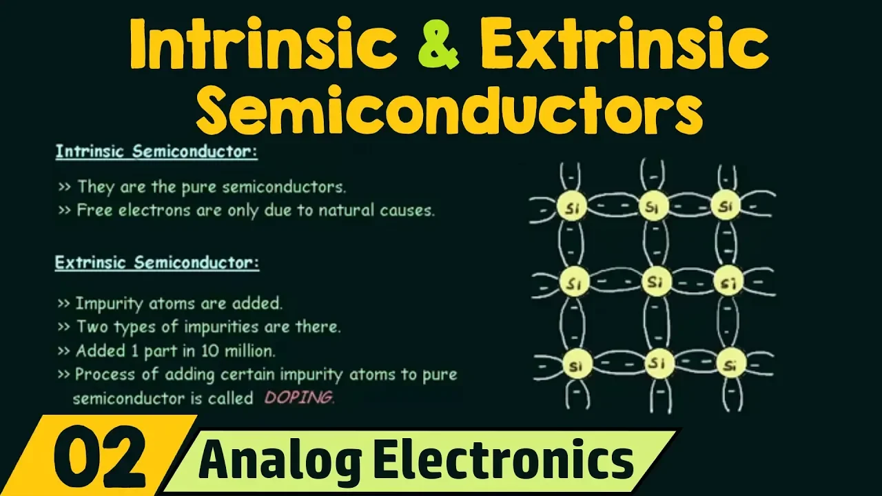
- Why this video: A comprehensive, classroom-style lecture detailing the structural and behavioral differences between pure intrinsic semiconductors and doped extrinsic semiconductors (-type and -type). It explains how thermal energy generates electron-hole pairs and how dopants alter charge carrier concentration.

- Why this video: A 3D animation that visualizes the substitution of Silicon atoms (4 valence electrons) with pentavalent dopants like Phosphorus (yielding an extra free electron) and trivalent dopants like Boron (yielding an empty electron state, or hole) in the lattice.

- Why this video: This video focuses on the concept of "holes" in semiconductor physics. It explains that a hole is not just the absence of an electron, but a mathematical and physical quasiparticle with a positive charge, mass, and momentum that moves through the valence band as valence electrons step sequentially into empty positions.
Knowledge Checkpoint
- Explain how adding a pentavalent impurity (e.g., Phosphorus) creates an -type semiconductor, and where its donor energy level () lies relative to the conduction band.
- Explain how adding a trivalent impurity (e.g., Boron) creates a -type semiconductor, and where its acceptor energy level () lies relative to the valence band.
- Define the physical nature of a "hole" in the valence band, explaining how its motion constitutes an electrical current.
Module 4: The P-N Junction and Diode Mechanics
When -type and -type materials are brought into physical contact, they do not remain passive. Instead, a dynamic boundary layer called the - junction forms. This module covers carrier diffusion and drift, the emergence of the depletion region, the establishment of the built-in barrier potential, and how the system behaves under external forward and reverse bias.
Recommended Videos

- Why this video: An exceptionally clear visual animation that details the step-by-step formation of the depletion region. It illustrates majority carriers diffusing across the junction, leaving behind ionized dopant atoms that create a localized electric field, which eventually halts further diffusion.

- Why this video: This video directly addresses the core physics gap identified in the review: providing a clear explanation of carrier transport under drift (driven by an electric field) versus diffusion (driven by carrier concentration gradients). This distinction is vital for understanding equilibrium in a - junction.
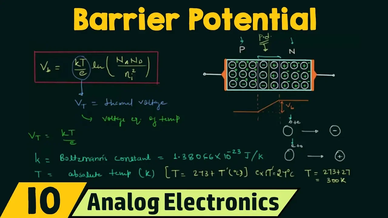
- Why this video: A highly structured academic breakdown of the barrier potential (). It explains how the electric field in the depletion zone creates a potential barrier, preventing further majority carrier diffusion, and how this barrier varies with temperature and doping concentration.
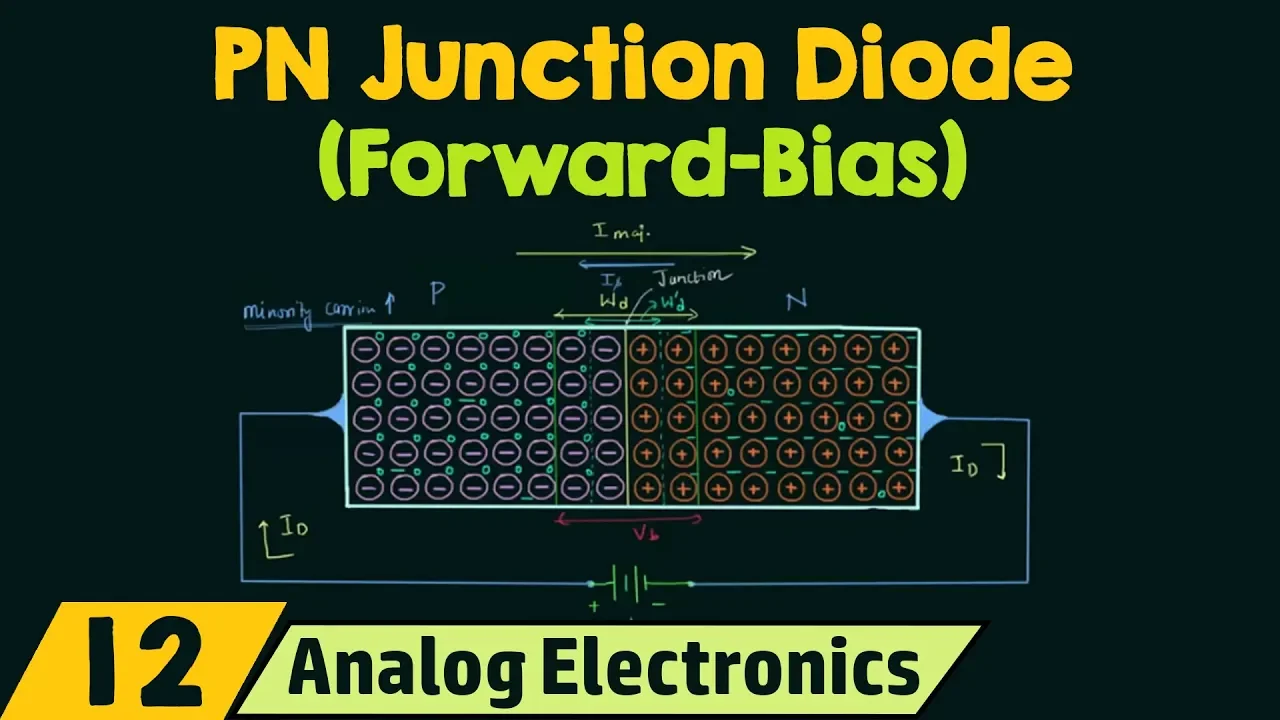
- Why this video: This lecture explains what happens when an external voltage is applied. It details how forward bias opposes the built-in potential barrier, narrowing the depletion region and allowing a large diffusion current to flow, while reverse bias widens the barrier, blocking current except for a tiny minority-carrier leakage current.
Knowledge Checkpoint
- Differentiate between drift current and diffusion current, identifying the driving force behind each mechanism.
- Explain how the ionized donor () and acceptor () impurities left behind in the depletion region create a built-in electric field that halts majority carrier diffusion.
- Describe the changes in depletion width and energy band alignment across a - junction when subjected to forward bias versus reverse bias.
Module 5: MOSFETs and Modern Transistor Physics
The Metal-Oxide-Semiconductor Field-Effect Transistor (MOSFET) is the basic switch of modern digital electronics. This module explores how an external gate voltage modulates the electrical conductivity of a semiconductor channel via electrostatic field effects, enabling modern integrated circuits. We will also address physical scaling limits and the challenges facing Moore's Law.
Recommended Videos
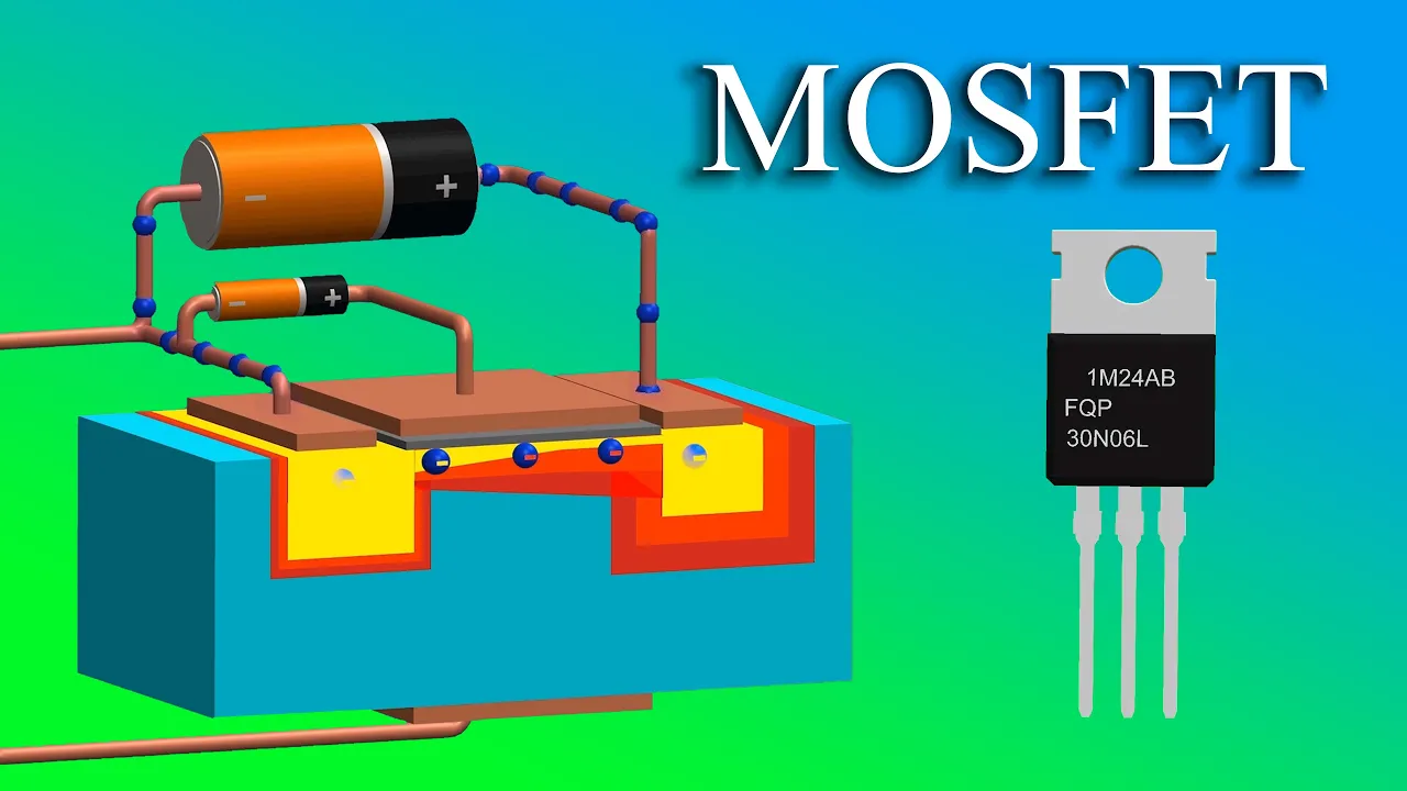
- Why this video: This video provides an excellent 3D visual explanation of an -channel enhancement MOSFET. It shows how positive gate voltage repels holes in the -type substrate and attracts electrons to form a thin, conductive inversion layer (channel) between the source and drain terminals.

- Why this video: For students seeking true engineering depth, Professor Behzad Razavi of UCLA provides an unmatched academic lecture on the physical operation of MOSFETs. He covers threshold voltage (), pinch-off, channel-length modulation, and derives the fundamental current-voltage (-) equations for the cutoff, triode, and saturation regions.
- Why this video: This video connects the microscopic physics of transistors to the macroscopic scaling trends of Moore's Law. It explains how shrinking transistors to the nanometer scale leads to issues like quantum tunneling through thin gate oxides and high leakage currents, which threaten the limits of classical silicon computing.
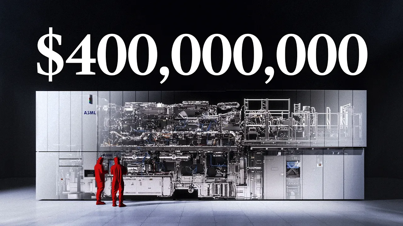
- Why this video: An incredibly produced documentary exploring extreme ultraviolet (EUV) photolithography—the manufacturing technology used to print billions of nanometer-scale transistors onto silicon wafers. It illustrates the engineering achievements required to keep Moore's Law alive today.
Knowledge Checkpoint
- Describe the process of inversion in a -type substrate under a positive gate voltage, explaining how the -channel is formed.
- Define the threshold voltage () and describe how the channel changes when .
- Explain the physical cause of "pinch-off" in a MOSFET channel when the drain-to-source voltage is increased, and how this leads to drain-current saturation.
- Discuss the physical limitations encountered when scaling silicon MOSFET gate oxides below several nanometers, focusing on quantum tunneling.
Course Map
Below is the recommended path through the curriculum. Each module serves as a direct conceptual prerequisite for the next.
Key People Index
- Niels Bohr (1885–1962): Danish physicist who developed the Bohr model of the atom in 1913, introducing the concept of quantized electron orbits.
- Erwin Schrödinger (1887–1961): Austrian physicist who formulated the wave equation in 1925, laying the foundation for quantum wave mechanics and atomic orbital theory.
- Ralph de Laer Kronig & William Penney: Physicists who proposed the Kronig-Penney Model in 1931, showing how a periodic potential creates forbidden energy gaps.
- Gordon Moore (1929–2023): Co-founder of Intel, who observed in 1965 that the number of transistors on a microchip doubles roughly every two years (Moore's Law).
- Dr. Behzad Razavi: Professor of Electrical Engineering at UCLA, renowned for his work in analog microelectronics design and education.
Final Self-Assessment
Complete this comprehensive self-assessment to verify your mastery of semiconductor physics:
- I can derive or explain the energy level quantization formula for a hydrogenic atom using the Bohr model.
- I can explain the physical process of band-gap formation using the concept of atomic orbital overlap (LCAO).
- I can explain why a crystal lattice's periodic potential creates forbidden band gaps, citing the Kronig-Penney model.
- I can distinguish between -type and -type semiconductors in terms of dopant valency, donor/acceptor energy levels, and majority/minority carriers.
- I can describe the mathematical and physical difference between electron drift and electron diffusion.
- I can explain the exact sequence of events that forms the depletion region when a -type and -type semiconductor are brought into contact.
- I can explain why a - junction allows current to flow easily under forward bias but blocks current under reverse bias.
- I can explain the electrostatic mechanism by which a gate voltage controls current flow in an -channel enhancement MOSFET.
- I can sketch the typical - characteristics of a MOSFET and mathematically identify the cutoff, triode, and saturation regions.
- I can name at least two major quantum or thermal limits encountered when scaling modern silicon transistors to the sub-5nm scale (e.g., gate leakage, subthreshold swing limits).